EP1585169A1 - Belichtungssystem und belichtungsverfahren - Google Patents
Belichtungssystem und belichtungsverfahren Download PDFInfo
- Publication number
- EP1585169A1 EP1585169A1 EP04701103A EP04701103A EP1585169A1 EP 1585169 A1 EP1585169 A1 EP 1585169A1 EP 04701103 A EP04701103 A EP 04701103A EP 04701103 A EP04701103 A EP 04701103A EP 1585169 A1 EP1585169 A1 EP 1585169A1
- Authority
- EP
- European Patent Office
- Prior art keywords
- mask
- optical system
- field stop
- illumination
- projection
- Prior art date
- Legal status (The legal status is an assumption and is not a legal conclusion. Google has not performed a legal analysis and makes no representation as to the accuracy of the status listed.)
- Granted
Links
Images


Classifications
-
- G—PHYSICS
- G03—PHOTOGRAPHY; CINEMATOGRAPHY; ANALOGOUS TECHNIQUES USING WAVES OTHER THAN OPTICAL WAVES; ELECTROGRAPHY; HOLOGRAPHY
- G03F—PHOTOMECHANICAL PRODUCTION OF TEXTURED OR PATTERNED SURFACES, e.g. FOR PRINTING, FOR PROCESSING OF SEMICONDUCTOR DEVICES; MATERIALS THEREFOR; ORIGINALS THEREFOR; APPARATUS SPECIALLY ADAPTED THEREFOR
- G03F7/00—Photomechanical, e.g. photolithographic, production of textured or patterned surfaces, e.g. printing surfaces; Materials therefor, e.g. comprising photoresists; Apparatus specially adapted therefor
- G03F7/70—Microphotolithographic exposure; Apparatus therefor
- G03F7/70058—Mask illumination systems
- G03F7/70066—Size and form of the illuminated area in the mask plane, e.g. reticle masking blades or blinds
-
- G—PHYSICS
- G03—PHOTOGRAPHY; CINEMATOGRAPHY; ANALOGOUS TECHNIQUES USING WAVES OTHER THAN OPTICAL WAVES; ELECTROGRAPHY; HOLOGRAPHY
- G03F—PHOTOMECHANICAL PRODUCTION OF TEXTURED OR PATTERNED SURFACES, e.g. FOR PRINTING, FOR PROCESSING OF SEMICONDUCTOR DEVICES; MATERIALS THEREFOR; ORIGINALS THEREFOR; APPARATUS SPECIALLY ADAPTED THEREFOR
- G03F7/00—Photomechanical, e.g. photolithographic, production of textured or patterned surfaces, e.g. printing surfaces; Materials therefor, e.g. comprising photoresists; Apparatus specially adapted therefor
- G03F7/70—Microphotolithographic exposure; Apparatus therefor
- G03F7/70058—Mask illumination systems
- G03F7/702—Reflective illumination, i.e. reflective optical elements other than folding mirrors, e.g. extreme ultraviolet [EUV] illumination systems
-
- G—PHYSICS
- G03—PHOTOGRAPHY; CINEMATOGRAPHY; ANALOGOUS TECHNIQUES USING WAVES OTHER THAN OPTICAL WAVES; ELECTROGRAPHY; HOLOGRAPHY
- G03F—PHOTOMECHANICAL PRODUCTION OF TEXTURED OR PATTERNED SURFACES, e.g. FOR PRINTING, FOR PROCESSING OF SEMICONDUCTOR DEVICES; MATERIALS THEREFOR; ORIGINALS THEREFOR; APPARATUS SPECIALLY ADAPTED THEREFOR
- G03F7/00—Photomechanical, e.g. photolithographic, production of textured or patterned surfaces, e.g. printing surfaces; Materials therefor, e.g. comprising photoresists; Apparatus specially adapted therefor
- G03F7/70—Microphotolithographic exposure; Apparatus therefor
- G03F7/70216—Mask projection systems
- G03F7/70283—Mask effects on the imaging process
-
- G—PHYSICS
- G03—PHOTOGRAPHY; CINEMATOGRAPHY; ANALOGOUS TECHNIQUES USING WAVES OTHER THAN OPTICAL WAVES; ELECTROGRAPHY; HOLOGRAPHY
- G03F—PHOTOMECHANICAL PRODUCTION OF TEXTURED OR PATTERNED SURFACES, e.g. FOR PRINTING, FOR PROCESSING OF SEMICONDUCTOR DEVICES; MATERIALS THEREFOR; ORIGINALS THEREFOR; APPARATUS SPECIALLY ADAPTED THEREFOR
- G03F7/00—Photomechanical, e.g. photolithographic, production of textured or patterned surfaces, e.g. printing surfaces; Materials therefor, e.g. comprising photoresists; Apparatus specially adapted therefor
- G03F7/70—Microphotolithographic exposure; Apparatus therefor
- G03F7/70216—Mask projection systems
- G03F7/70358—Scanning exposure, i.e. relative movement of patterned beam and workpiece during imaging
Definitions
- This invention relates to exposure systems and exposure methods, and in particular relates to exposure systems that are suitable for manufacturing of semiconductor devices and other microdevices using photolithography processes employing extreme ultraviolet (EUV) light having a wavelength of approximately 5 to 40 nm.
- EUV extreme ultraviolet
- a reflection-type projection-optical system comprising only reflecting optical members, must be employed.
- a reflection-type mask is used rather than a transmission-type mask, which requires that the illumination light be made incident obliquely to the mask. If the illumination light were made normally incident to a reflection-type mask, the optical path of the illumination light incident on the mask and the optical path of the illumination light reflected by the mask and propagating toward a projection-optical system would completely overlap. As a result, either the optical members of the illumination-optical system for illuminating the mask would block the optical path of the projection-optical system, or the optical members of the projection-optical system would block the optical path of the illumination-optical system.
- the reflectivity per reflection surface is low in an EUVL exposure system.
- the number of reflections in the optical system between the light source and the photosensitive substrate that is, in the illumination-optical system and in the projection-optical system
- an image-forming reflective optical system is situated between the mask and the field stop as explained above. The resulting high number of reflections in the optical path of the illumination-optical system results in substantial loss of light, which prevents achievement of the necessary throughput.
- the interval between the mask and the field stop is i n
- the numerical aperture on the mask side of the projection-optical system is NA
- the width dimension of the aperture portion of the field stop along the prescribed direction is w
- the angle of incidence (in radians) on the mask of the principal ray of the illumination light illuminating the mask is a n
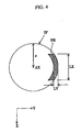
- the radiation flux from the area "e” on the mask M, as incident on the projection-optical system having a numerical aperture NA pro on the mask side (object side), is not blocked at all by the field stop FS.
- radiation flux incident on the projection-optical system from the areas “d” and “f” on either side of the area “e” is partially blocked by the field stop FS.
- the extent of blocking, by the field stop FS, of flux from the areas “d” and "f” on either side increases substantially as the outer edge of the areas "d” and "f” is approached.
- the image-forming radiation flux contributing to exposure through the projection-optical system is flux that is incident on and reflected by the area on the mask M in which the area "b" and the area "e” overlap, and on the areas "a” and "f".
- the acceptable tolerance for variation in the line-widths of independent lines is approximately 10 % of these designed line-widths to ensure reliable operation.
- line-width variations arising from the exposure system must be kept to 3 % or less.
- the line-width variation arising from the field stop must be held to within, at most, 1 %.
- the width of the area "f" and the width "g" of the effective illumination area are respectively represented by the following equations (3) and (4).
- equation (7) The diffracted light amplitude D( ⁇ , ⁇ ) at the entrance pupil of the projection-optical system is given by equation (7) below.
- ( ⁇ , ⁇ ) are coordinates on the entrance pupil of the projection-optical system
- (x,y) are coordinates on the mask
- M(x,y) is the mask-amplitude transmissivity
- k is a constant represented by 2 ⁇ / ⁇
- ⁇ indicates a double integral evaluated over the field of the mask.
- the light-intensity distribution I(X,Y) on the photosensitive substrate is expressed by the following equation (8).
- (X,Y) are coordinates on the photosensitive substrate
- ( ⁇ , ⁇ ) are coordinates on the effective extended source formed at the exit pupil of the illumination system
- U( ⁇ , ⁇ ) is the light-intensity distribution of the extended source
- ⁇ ( ⁇ , ⁇ ,x,y) is the image-forming magnification at the entrance pupil of the projection-optical system from the extended source
- W( ⁇ , ⁇ ,X,Y) is the wavefront of the projection-optical system
- the first occurrence of ⁇ represents a double integral over the extended source
- the second occurrence of ⁇ represents a double integral over the image-side numerical aperture NA of the projection-optical system.
- a configuration is adopted in which a field stop used for defining the illumination area on the mask is positioned in proximity to the mask. But, because the interval i n between the mask and the field stop is set so as to satisfy conditional relations (5) or (6), any adverse effect of the blockage of light by the field stop on the image-forming performance of the projection-optical system can be satisfactorily minimized. Further, a configuration is adopted in which the field stop is positioned in proximity to the mask, so that there is no need to insert an image-forming reflective optical system between the mask and field stop. Also, the number of reflections in the optical path of the illumination-optical system can be decreased, thereby reducing optical losses and achieving the necessary throughput.
- the interval i n between the mask and field stop satisfy the conditional relation (9). In such a configuration, even if an integral multiple of the amount of mask-scan movement per light pulse does not exactly coincide with the width w in the scan direction of the illumination area on the mask, a substantially uniform distribution of cumulative exposure dose on the photosensitive substrate can be obtained.
- the wafer W is held by a wafer stage 7, which is movable in two dimensions along the X and Y directions, so that the exposure surface extends in the XY plane.
- a wafer stage 7 As the mask stage 5, movement of the wafer stage 7 is measured by a laser interferometer 8.
- the pattern of the mask M is transferred to a single exposure area of the wafer W.
- the movement velocity of the wafer stage 7 is set to 1/4 the movement velocity of the mask stage 5 during synchronous scanning.
- the pattern of the mask M is transferred to each of the exposure areas of the wafer W.
- the interval i n between the mask M and the field stop 19 is set so as to satisfy conditional relation (9).
- the effect on the image-forming performance of the projection-optical system PL can be satisfactorily controlled, and the mask pattern can be transferred onto the wafer W accurately and with high throughput.
- a laser plasma light source is used as the light source to supply EUV light. It will be understood that the light source is not limited to such a source; other appropriate light sources can be used instead.
- a configuration is adopted in which a field stop, used for defining the illumination area on a mask, is positioned in proximity to the mask. But, the interval between the mask and the field stop is set so as to satisfy a prescribed conditional relation. Consequently, the effect of light blockage by the field stop on the image-forming performance of the projection-optical system can be satisfactorily controlled. Also, because a configuration is adopted in which the field stop is positioned in proximity to the mask, there is no need to insert an image-forming reflective optical system between the mask and field stop. Thus, the number of reflections in the optical path of the illumination-optical system can be decreased, light losses can be reduced, and the necessary throughput can be achieved.
Landscapes
- Physics & Mathematics (AREA)
- General Physics & Mathematics (AREA)
- Exposure And Positioning Against Photoresist Photosensitive Materials (AREA)
- Exposure Of Semiconductors, Excluding Electron Or Ion Beam Exposure (AREA)
- Liquid Crystal Substances (AREA)
Applications Claiming Priority (3)
| Application Number | Priority Date | Filing Date | Title |
|---|---|---|---|
| JP2003003868 | 2003-01-10 | ||
| JP2003003868 | 2003-01-10 | ||
| PCT/JP2004/000129 WO2004064128A1 (ja) | 2003-01-10 | 2004-01-09 | 露光装置および露光方法 |
Publications (3)
| Publication Number | Publication Date |
|---|---|
| EP1585169A1 true EP1585169A1 (de) | 2005-10-12 |
| EP1585169A4 EP1585169A4 (de) | 2007-07-18 |
| EP1585169B1 EP1585169B1 (de) | 2009-11-18 |
Family
ID=32708922
Family Applications (1)
| Application Number | Title | Priority Date | Filing Date |
|---|---|---|---|
| EP04701103A Expired - Lifetime EP1585169B1 (de) | 2003-01-10 | 2004-01-09 | Belichtungssystem und belichtungsverfahren |
Country Status (6)
| Country | Link |
|---|---|
| US (1) | US7023523B2 (de) |
| EP (1) | EP1585169B1 (de) |
| JP (1) | JP4822417B2 (de) |
| AT (1) | ATE449417T1 (de) |
| DE (1) | DE602004024168D1 (de) |
| WO (1) | WO2004064128A1 (de) |
Families Citing this family (5)
| Publication number | Priority date | Publication date | Assignee | Title |
|---|---|---|---|---|
| US7312851B2 (en) * | 2004-06-23 | 2007-12-25 | Nikon Corporation | Projection optical system, exposure apparatus, and exposure method in which a reflective projection optical system has a non-circular aperture stop |
| JP5007538B2 (ja) * | 2006-08-30 | 2012-08-22 | 株式会社ニコン | 露光装置、デバイスの製造方法及び露光方法 |
| DE102008002377A1 (de) | 2007-07-17 | 2009-01-22 | Carl Zeiss Smt Ag | Beleuchtungssystem sowie Projektionsbelichtungsanlage für die Mikrolithografie mit einem derartigen Beleuchtungssystem |
| JP5061063B2 (ja) * | 2008-05-20 | 2012-10-31 | ギガフォトン株式会社 | 極端紫外光用ミラーおよび極端紫外光源装置 |
| KR101944655B1 (ko) * | 2010-04-02 | 2019-01-31 | 가부시키가이샤 니콘 | 조명 광학계, 광학 장치, 노광 방법 및 디바이스 제조 방법 |
Family Cites Families (12)
| Publication number | Priority date | Publication date | Assignee | Title |
|---|---|---|---|---|
| US5315629A (en) * | 1990-10-10 | 1994-05-24 | At&T Bell Laboratories | Ringfield lithography |
| US5583609A (en) * | 1993-04-23 | 1996-12-10 | Nikon Corporation | Projection exposure apparatus |
| US5729331A (en) * | 1993-06-30 | 1998-03-17 | Nikon Corporation | Exposure apparatus, optical projection apparatus and a method for adjusting the optical projection apparatus |
| JP3057998B2 (ja) * | 1994-02-16 | 2000-07-04 | キヤノン株式会社 | 照明装置及びそれを用いた投影露光装置 |
| JP3358097B2 (ja) * | 1994-04-12 | 2002-12-16 | 株式会社ニコン | X線投影露光装置 |
| JP3624523B2 (ja) * | 1996-03-06 | 2005-03-02 | 株式会社ニコン | X線投影露光装置 |
| JPH1092727A (ja) * | 1996-09-11 | 1998-04-10 | Canon Inc | 投影露光装置 |
| JP2000091220A (ja) * | 1998-09-08 | 2000-03-31 | Nikon Corp | 投影露光装置及び投影露光方法 |
| JP2000286191A (ja) * | 1999-03-31 | 2000-10-13 | Nikon Corp | 露光装置および露光方法ならびにデバイス製造方法 |
| JP2000349009A (ja) * | 1999-06-04 | 2000-12-15 | Nikon Corp | 露光方法及び装置 |
| JP2000356855A (ja) * | 1999-06-15 | 2000-12-26 | Nikon Corp | 照明領域設定装置および露光装置 |
| JP3363882B2 (ja) * | 2000-10-17 | 2003-01-08 | 株式会社日立製作所 | 露光装置 |
-
2004
- 2004-01-09 WO PCT/JP2004/000129 patent/WO2004064128A1/ja not_active Ceased
- 2004-01-09 JP JP2005507991A patent/JP4822417B2/ja not_active Expired - Fee Related
- 2004-01-09 AT AT04701103T patent/ATE449417T1/de not_active IP Right Cessation
- 2004-01-09 DE DE602004024168T patent/DE602004024168D1/de not_active Expired - Lifetime
- 2004-01-09 EP EP04701103A patent/EP1585169B1/de not_active Expired - Lifetime
-
2005
- 2005-07-07 US US11/177,141 patent/US7023523B2/en not_active Expired - Lifetime
Also Published As
| Publication number | Publication date |
|---|---|
| JPWO2004064128A1 (ja) | 2006-05-18 |
| EP1585169B1 (de) | 2009-11-18 |
| JP4822417B2 (ja) | 2011-11-24 |
| US20050264789A1 (en) | 2005-12-01 |
| ATE449417T1 (de) | 2009-12-15 |
| DE602004024168D1 (de) | 2009-12-31 |
| WO2004064128A1 (ja) | 2004-07-29 |
| EP1585169A4 (de) | 2007-07-18 |
| US7023523B2 (en) | 2006-04-04 |
Similar Documents
| Publication | Publication Date | Title |
|---|---|---|
| JP3862347B2 (ja) | X線縮小露光装置およびこれを利用したデバイス製造方法 | |
| JP3259657B2 (ja) | 投影露光装置及びそれを用いたデバイスの製造方法 | |
| US10120176B2 (en) | Catadioptric projection objective comprising deflection mirrors and projection exposure method | |
| KR100585461B1 (ko) | 마이크로리소그래피 투영장치 | |
| JP3413160B2 (ja) | 照明装置及びそれを用いた走査型露光装置 | |
| JPH07176475A (ja) | 投影露光装置及び該投影露光装置を用いたデバイスの製造方法 | |
| KR20080056094A (ko) | 노광 장치 및 디바이스 제조 방법 | |
| JP5509933B2 (ja) | オプティカルインテグレータ、照明光学系、露光装置、およびデバイス製造方法 | |
| US20140377692A1 (en) | Mask for microlithography and scanning projection exposure method utilizing the mask | |
| KR101501303B1 (ko) | 조명 광학 장치, 노광 장치, 및 디바이스 제조 방법 | |
| JP4924421B2 (ja) | センサの校正方法、露光方法、露光装置、デバイス製造方法、および反射型マスク | |
| EP1517339A2 (de) | Optisches Beleuchtungssystem und Belichtungsanlage | |
| KR20040090734A (ko) | 리소그래피 장치 및 디바이스 제조방법 | |
| EP1585169B1 (de) | Belichtungssystem und belichtungsverfahren | |
| US6573977B1 (en) | Exposure control method, exposure apparatus and device manufacturing method | |
| JP2004170869A (ja) | 結像光学系、露光装置および露光方法 | |
| JP3958122B2 (ja) | 照明装置、およびそれを用いた露光装置、デバイス製造方法 | |
| JP2004356291A (ja) | 走査露光装置及び走査露光方法 | |
| JP2000133563A (ja) | 露光方法及び露光装置 | |
| JP2007189079A (ja) | 照明光学系、当該照明光学系を有する露光装置及びデバイス製造方法 | |
| JP2011150227A (ja) | 露光装置、およびデバイス製造方法 | |
| JP2005072513A (ja) | 露光装置および露光方法 | |
| JP2006128366A (ja) | 露光装置、露光方法、およびデバイスの製造方法 | |
| WO2010073801A1 (ja) | 照明光学系、露光装置及びデバイスの製造方法 |
Legal Events
| Date | Code | Title | Description |
|---|---|---|---|
| PUAI | Public reference made under article 153(3) epc to a published international application that has entered the european phase |
Free format text: ORIGINAL CODE: 0009012 |
|
| 17P | Request for examination filed |
Effective date: 20050707 |
|
| AK | Designated contracting states |
Kind code of ref document: A1 Designated state(s): AT BE BG CH CY CZ DE DK EE ES FI FR GB GR HU IE IT LI LU MC NL PT RO SE SI SK TR |
|
| AX | Request for extension of the european patent |
Extension state: AL LT LV MK |
|
| DAX | Request for extension of the european patent (deleted) | ||
| A4 | Supplementary search report drawn up and despatched |
Effective date: 20070619 |
|
| GRAP | Despatch of communication of intention to grant a patent |
Free format text: ORIGINAL CODE: EPIDOSNIGR1 |
|
| GRAS | Grant fee paid |
Free format text: ORIGINAL CODE: EPIDOSNIGR3 |
|
| GRAA | (expected) grant |
Free format text: ORIGINAL CODE: 0009210 |
|
| AK | Designated contracting states |
Kind code of ref document: B1 Designated state(s): AT BE BG CH CY CZ DE DK EE ES FI FR GB GR HU IE IT LI LU MC NL PT RO SE SI SK TR |
|
| REG | Reference to a national code |
Ref country code: GB Ref legal event code: FG4D |
|
| REG | Reference to a national code |
Ref country code: CH Ref legal event code: EP |
|
| REG | Reference to a national code |
Ref country code: IE Ref legal event code: FG4D |
|
| REF | Corresponds to: |
Ref document number: 602004024168 Country of ref document: DE Date of ref document: 20091231 Kind code of ref document: P |
|
| PG25 | Lapsed in a contracting state [announced via postgrant information from national office to epo] |
Ref country code: SE Free format text: LAPSE BECAUSE OF FAILURE TO SUBMIT A TRANSLATION OF THE DESCRIPTION OR TO PAY THE FEE WITHIN THE PRESCRIBED TIME-LIMIT Effective date: 20091118 Ref country code: FI Free format text: LAPSE BECAUSE OF FAILURE TO SUBMIT A TRANSLATION OF THE DESCRIPTION OR TO PAY THE FEE WITHIN THE PRESCRIBED TIME-LIMIT Effective date: 20091118 Ref country code: ES Free format text: LAPSE BECAUSE OF FAILURE TO SUBMIT A TRANSLATION OF THE DESCRIPTION OR TO PAY THE FEE WITHIN THE PRESCRIBED TIME-LIMIT Effective date: 20100228 Ref country code: PT Free format text: LAPSE BECAUSE OF FAILURE TO SUBMIT A TRANSLATION OF THE DESCRIPTION OR TO PAY THE FEE WITHIN THE PRESCRIBED TIME-LIMIT Effective date: 20100318 |
|
| PG25 | Lapsed in a contracting state [announced via postgrant information from national office to epo] |
Ref country code: SI Free format text: LAPSE BECAUSE OF FAILURE TO SUBMIT A TRANSLATION OF THE DESCRIPTION OR TO PAY THE FEE WITHIN THE PRESCRIBED TIME-LIMIT Effective date: 20091118 Ref country code: CY Free format text: LAPSE BECAUSE OF FAILURE TO SUBMIT A TRANSLATION OF THE DESCRIPTION OR TO PAY THE FEE WITHIN THE PRESCRIBED TIME-LIMIT Effective date: 20091118 |
|
| PG25 | Lapsed in a contracting state [announced via postgrant information from national office to epo] |
Ref country code: AT Free format text: LAPSE BECAUSE OF FAILURE TO SUBMIT A TRANSLATION OF THE DESCRIPTION OR TO PAY THE FEE WITHIN THE PRESCRIBED TIME-LIMIT Effective date: 20091118 Ref country code: BE Free format text: LAPSE BECAUSE OF FAILURE TO SUBMIT A TRANSLATION OF THE DESCRIPTION OR TO PAY THE FEE WITHIN THE PRESCRIBED TIME-LIMIT Effective date: 20091118 |
|
| RAP2 | Party data changed (patent owner data changed or rights of a patent transferred) |
Owner name: NIKON CORPORATION |
|
| PG25 | Lapsed in a contracting state [announced via postgrant information from national office to epo] |
Ref country code: EE Free format text: LAPSE BECAUSE OF FAILURE TO SUBMIT A TRANSLATION OF THE DESCRIPTION OR TO PAY THE FEE WITHIN THE PRESCRIBED TIME-LIMIT Effective date: 20091118 Ref country code: DK Free format text: LAPSE BECAUSE OF FAILURE TO SUBMIT A TRANSLATION OF THE DESCRIPTION OR TO PAY THE FEE WITHIN THE PRESCRIBED TIME-LIMIT Effective date: 20091118 Ref country code: BG Free format text: LAPSE BECAUSE OF FAILURE TO SUBMIT A TRANSLATION OF THE DESCRIPTION OR TO PAY THE FEE WITHIN THE PRESCRIBED TIME-LIMIT Effective date: 20100218 Ref country code: RO Free format text: LAPSE BECAUSE OF FAILURE TO SUBMIT A TRANSLATION OF THE DESCRIPTION OR TO PAY THE FEE WITHIN THE PRESCRIBED TIME-LIMIT Effective date: 20091118 |
|
| PG25 | Lapsed in a contracting state [announced via postgrant information from national office to epo] |
Ref country code: CZ Free format text: LAPSE BECAUSE OF FAILURE TO SUBMIT A TRANSLATION OF THE DESCRIPTION OR TO PAY THE FEE WITHIN THE PRESCRIBED TIME-LIMIT Effective date: 20091118 Ref country code: SK Free format text: LAPSE BECAUSE OF FAILURE TO SUBMIT A TRANSLATION OF THE DESCRIPTION OR TO PAY THE FEE WITHIN THE PRESCRIBED TIME-LIMIT Effective date: 20091118 Ref country code: MC Free format text: LAPSE BECAUSE OF NON-PAYMENT OF DUE FEES Effective date: 20100131 |
|
| REG | Reference to a national code |
Ref country code: CH Ref legal event code: PL |
|
| PLBE | No opposition filed within time limit |
Free format text: ORIGINAL CODE: 0009261 |
|
| STAA | Information on the status of an ep patent application or granted ep patent |
Free format text: STATUS: NO OPPOSITION FILED WITHIN TIME LIMIT |
|
| REG | Reference to a national code |
Ref country code: FR Ref legal event code: ST Effective date: 20100930 |
|
| 26N | No opposition filed |
Effective date: 20100819 |
|
| GBPC | Gb: european patent ceased through non-payment of renewal fee |
Effective date: 20100218 |
|
| PG25 | Lapsed in a contracting state [announced via postgrant information from national office to epo] |
Ref country code: FR Free format text: LAPSE BECAUSE OF NON-PAYMENT OF DUE FEES Effective date: 20100201 Ref country code: GR Free format text: LAPSE BECAUSE OF FAILURE TO SUBMIT A TRANSLATION OF THE DESCRIPTION OR TO PAY THE FEE WITHIN THE PRESCRIBED TIME-LIMIT Effective date: 20100219 Ref country code: LI Free format text: LAPSE BECAUSE OF NON-PAYMENT OF DUE FEES Effective date: 20100131 Ref country code: CH Free format text: LAPSE BECAUSE OF NON-PAYMENT OF DUE FEES Effective date: 20100131 |
|
| PG25 | Lapsed in a contracting state [announced via postgrant information from national office to epo] |
Ref country code: IE Free format text: LAPSE BECAUSE OF NON-PAYMENT OF DUE FEES Effective date: 20100109 |
|
| PG25 | Lapsed in a contracting state [announced via postgrant information from national office to epo] |
Ref country code: GB Free format text: LAPSE BECAUSE OF NON-PAYMENT OF DUE FEES Effective date: 20100218 Ref country code: IT Free format text: LAPSE BECAUSE OF FAILURE TO SUBMIT A TRANSLATION OF THE DESCRIPTION OR TO PAY THE FEE WITHIN THE PRESCRIBED TIME-LIMIT Effective date: 20091118 |
|
| PG25 | Lapsed in a contracting state [announced via postgrant information from national office to epo] |
Ref country code: HU Free format text: LAPSE BECAUSE OF FAILURE TO SUBMIT A TRANSLATION OF THE DESCRIPTION OR TO PAY THE FEE WITHIN THE PRESCRIBED TIME-LIMIT Effective date: 20100519 Ref country code: LU Free format text: LAPSE BECAUSE OF NON-PAYMENT OF DUE FEES Effective date: 20100109 |
|
| PG25 | Lapsed in a contracting state [announced via postgrant information from national office to epo] |
Ref country code: TR Free format text: LAPSE BECAUSE OF FAILURE TO SUBMIT A TRANSLATION OF THE DESCRIPTION OR TO PAY THE FEE WITHIN THE PRESCRIBED TIME-LIMIT Effective date: 20091118 |
|
| PGFP | Annual fee paid to national office [announced via postgrant information from national office to epo] |
Ref country code: NL Payment date: 20211216 Year of fee payment: 19 |
|
| PGFP | Annual fee paid to national office [announced via postgrant information from national office to epo] |
Ref country code: DE Payment date: 20211130 Year of fee payment: 19 |
|
| REG | Reference to a national code |
Ref country code: DE Ref legal event code: R119 Ref document number: 602004024168 Country of ref document: DE |
|
| REG | Reference to a national code |
Ref country code: NL Ref legal event code: MM Effective date: 20230201 |
|
| PG25 | Lapsed in a contracting state [announced via postgrant information from national office to epo] |
Ref country code: NL Free format text: LAPSE BECAUSE OF NON-PAYMENT OF DUE FEES Effective date: 20230201 Ref country code: DE Free format text: LAPSE BECAUSE OF NON-PAYMENT OF DUE FEES Effective date: 20230801 |