EP1585169B1 - Belichtungssystem und belichtungsverfahren - Google Patents
Belichtungssystem und belichtungsverfahren Download PDFInfo
- Publication number
- EP1585169B1 EP1585169B1 EP04701103A EP04701103A EP1585169B1 EP 1585169 B1 EP1585169 B1 EP 1585169B1 EP 04701103 A EP04701103 A EP 04701103A EP 04701103 A EP04701103 A EP 04701103A EP 1585169 B1 EP1585169 B1 EP 1585169B1
- Authority
- EP
- European Patent Office
- Prior art keywords
- mask
- optical system
- field stop
- illumination
- projection
- Prior art date
- Legal status (The legal status is an assumption and is not a legal conclusion. Google has not performed a legal analysis and makes no representation as to the accuracy of the status listed.)
- Expired - Lifetime
Links
Images


Classifications
-
- G—PHYSICS
- G03—PHOTOGRAPHY; CINEMATOGRAPHY; ANALOGOUS TECHNIQUES USING WAVES OTHER THAN OPTICAL WAVES; ELECTROGRAPHY; HOLOGRAPHY
- G03F—PHOTOMECHANICAL PRODUCTION OF TEXTURED OR PATTERNED SURFACES, e.g. FOR PRINTING, FOR PROCESSING OF SEMICONDUCTOR DEVICES; MATERIALS THEREFOR; ORIGINALS THEREFOR; APPARATUS SPECIALLY ADAPTED THEREFOR
- G03F7/00—Photomechanical, e.g. photolithographic, production of textured or patterned surfaces, e.g. printing surfaces; Materials therefor, e.g. comprising photoresists; Apparatus specially adapted therefor
- G03F7/70—Microphotolithographic exposure; Apparatus therefor
- G03F7/70058—Mask illumination systems
- G03F7/70066—Size and form of the illuminated area in the mask plane, e.g. reticle masking blades or blinds
-
- G—PHYSICS
- G03—PHOTOGRAPHY; CINEMATOGRAPHY; ANALOGOUS TECHNIQUES USING WAVES OTHER THAN OPTICAL WAVES; ELECTROGRAPHY; HOLOGRAPHY
- G03F—PHOTOMECHANICAL PRODUCTION OF TEXTURED OR PATTERNED SURFACES, e.g. FOR PRINTING, FOR PROCESSING OF SEMICONDUCTOR DEVICES; MATERIALS THEREFOR; ORIGINALS THEREFOR; APPARATUS SPECIALLY ADAPTED THEREFOR
- G03F7/00—Photomechanical, e.g. photolithographic, production of textured or patterned surfaces, e.g. printing surfaces; Materials therefor, e.g. comprising photoresists; Apparatus specially adapted therefor
- G03F7/70—Microphotolithographic exposure; Apparatus therefor
- G03F7/70058—Mask illumination systems
- G03F7/702—Reflective illumination, i.e. reflective optical elements other than folding mirrors, e.g. extreme ultraviolet [EUV] illumination systems
-
- G—PHYSICS
- G03—PHOTOGRAPHY; CINEMATOGRAPHY; ANALOGOUS TECHNIQUES USING WAVES OTHER THAN OPTICAL WAVES; ELECTROGRAPHY; HOLOGRAPHY
- G03F—PHOTOMECHANICAL PRODUCTION OF TEXTURED OR PATTERNED SURFACES, e.g. FOR PRINTING, FOR PROCESSING OF SEMICONDUCTOR DEVICES; MATERIALS THEREFOR; ORIGINALS THEREFOR; APPARATUS SPECIALLY ADAPTED THEREFOR
- G03F7/00—Photomechanical, e.g. photolithographic, production of textured or patterned surfaces, e.g. printing surfaces; Materials therefor, e.g. comprising photoresists; Apparatus specially adapted therefor
- G03F7/70—Microphotolithographic exposure; Apparatus therefor
- G03F7/70216—Mask projection systems
- G03F7/70283—Mask effects on the imaging process
-
- G—PHYSICS
- G03—PHOTOGRAPHY; CINEMATOGRAPHY; ANALOGOUS TECHNIQUES USING WAVES OTHER THAN OPTICAL WAVES; ELECTROGRAPHY; HOLOGRAPHY
- G03F—PHOTOMECHANICAL PRODUCTION OF TEXTURED OR PATTERNED SURFACES, e.g. FOR PRINTING, FOR PROCESSING OF SEMICONDUCTOR DEVICES; MATERIALS THEREFOR; ORIGINALS THEREFOR; APPARATUS SPECIALLY ADAPTED THEREFOR
- G03F7/00—Photomechanical, e.g. photolithographic, production of textured or patterned surfaces, e.g. printing surfaces; Materials therefor, e.g. comprising photoresists; Apparatus specially adapted therefor
- G03F7/70—Microphotolithographic exposure; Apparatus therefor
- G03F7/70216—Mask projection systems
- G03F7/70358—Scanning exposure, i.e. relative movement of patterned beam and workpiece during imaging
Definitions
- This invention relates to exposure systems and exposure methods, and in particular relates to exposure systems that are suitable for manufacturing of semiconductor devices and other microdevices using photolithography processes employing extreme ultraviolet (EUV) light having a wavelength of approximately 5 to 40 nm.
- EUV extreme ultraviolet
- a reflection-type projection-optical system comprising only reflecting optical members, must be employed.
- a reflection-type mask is used rather than a transmission-type mask, which requires that the illumination light be made incident obliquely to the mask. If the illumination light were made normally incident to a reflection-type mask, the optical path of the illumination light incident on the mask and the optical path of the illumination light reflected by the mask and propagating toward a projection-optical system would completely overlap. As a result, either the optical members of the illumination-optical system for illuminating the mask would block the optical path of the projection-optical system, or the optical members of the projection-optical system would block the optical path of the illumination-optical system.
- a narrow arc-shaped effective exposure area i . e ., stationary exposure area
- the mask and photosensitive substrate must be moved relative to the projection-optical system to scan the exposure light along the mask pattern over the photosensitive substrate (this is called "scanning exposure").
- a field stop used for defining the stationary exposure area must be placed at a position that is substantially optically conjugate with the photosensitive substrate.
- a field stop is provided in the optical path of the illumination-optical system.
- the reflectivity per reflection surface is low in an EUVL exposure system.
- the number of reflections in the optical system between the light source and the photosensitive substrate that is, in the illumination-optical system and in the projection-optical system
- an image-forming reflective optical system is situated between the mask and the field stop as explained above. The resulting high number of reflections in the optical path of the illumination-optical system results in substantial loss of light, which prevents achievement of the necessary throughput.
- a configuration may be adopted in which the field stop is positioned in proximity to the reflection-type mask.
- simply positioning the field stop in proximity to the reflection-type mask would cause a portion of the necessary radiation flux to be blocked by the field stop, with an adverse effect on the image-forming performance of the projection-optical system. This situation would raise the possibility that the mask pattern could not be transferred, accurately and without distortion, onto the photosensitive substrate.
- This invention was devised in light of the above-described problems, and has an object of providing an exposure system and exposure method that are capable of transferring a mask pattern onto a photosensitive substrate accurately and with high throughput, while satisfactorily controlling adverse effects, on the image-forming performance of the projection-optical system, despite the use of a field stop in proximity to the reflection-type mask.
- an exposure system comprising an illumination-optical system to illuminate a reflection-type mask on which is formed a prescribed pattern.
- the exposure system also comprises a projection-optical system to form an image of the mask pattern on a photosensitive substrate.
- the mask and the photosensitive substrate are moved relative to the projection-optical system in a prescribed direction to project the mask pattern onto and expose the photosensitive substrate.
- the exposure system is characterized in that the illumination-optical system has a field stop, positioned in proximity to the mask, to define the illumination area on the mask.
- the interval between the mask and the field stop is i n
- the numerical aperture on the mask side of the projection-optical system is NA
- the width dimension of the aperture portion of the field stop along the prescribed direction is w
- the angle of incidence (in radians) on the mask of the principal ray of the illumination light illuminating the mask is a n
- an exposure method comprises an illumination step in which a reflection-type mask, on which is formed a prescribed pattern, is illuminated.
- the mask and the photosensitive substrate are moved relative to the projection-optical system in a prescribed direction to project the mask pattern onto and expose the photosensitive substrate.
- the exposure method is characterized in that the illumination step comprises an illumination-area-definition step in which the illumination area on the mask is defined by using a field stop that is positioned in proximity to the mask.
- the interval between the mask and the field stop is i n
- the numerical aperture on the mask side of the projection-optical system is NA
- the width dimension of the aperture portion of the field stop along the prescribed direction is w
- the angle of incidence (in radians) on the mask of the principal ray of the illumination light illuminating the mask is a n
- FIG. 1 explains a difficulty occurring in a configuration in which a field stop FS is positioned in proximity to a reflection-type mask M.
- a field stop FS when radiation flux having numerical aperture NA ill is incident on the mask M through the field stop FS, the flux incident on the area “b” on the mask M is not blocked at all by the field stop FS. However, the flux incident on the areas “a” and “c” on either side of the area “b” is partially blocked by the field stop FS. Blocking of the radiation flux incident on the areas “a” and “c” by the field stop FS increases substantially as the outer edge of the areas "a” and "c” is approached.
- the radiation flux from the area "e” on the mask M, as incident on the projection-optical system having a numerical aperture NA pro on the mask side (object side), is not blocked at all by the field stop FS.
- radiation flux incident on the projection-optical system from the areas “d” and “f” on either side of the area “e” is partially blocked by the field stop FS.
- the extent of blocking, by the field stop FS, of flux from the areas “d” and "f” on either side increases substantially as the outer edge of the areas "d” and "f” is approached.
- the image-forming radiation flux contributing to exposure through the projection-optical system is flux that is incident on and reflected by the area on the mask M in which the area "b" and the area "e” overlap, and on the areas "a” and "f".
- the acceptable tolerance for variation in the line-widths of independent lines is approximately 10 % of these designed line-widths to ensure reliable operation.
- line-width variations arising from the exposure system must be kept to 3 % or less.
- the line-width variation arising from the field stop must be held to within, at most, 1 %.
- the image-forming radiation flux contributing to exposure through the projection-optical system is flux that has been incident on and reflected from the area of overlap on the mask M of areas "b" and “e,” and from the areas "a” and "f'.
- the radiation flux incident on and reflected from the area of overlap of areas "b” and “e” enables exposure by means of normal image formation through the projection-optical system.
- the radiation flux incident on and reflected from the area "f" has the greatest adverse influence on image formation through the projection-optical system.
- one criterion for satisfactorily controlling the effect on image-forming performance of the projection-optical system is the extent to which the width of the area "f" can be reduced relative to the interval "g" between the center of area "a” and the center of area “f” in FIG. 1 .
- the width "g" of the effective illumination area optically corresponds to the width (the dimension along the scan direction) of the effective exposure area.
- the extent of the adverse effect on the image-forming performance of the projection-optical system of radiation flux incident on and reflected by the area "f" depends on the image-side numerical aperture NA i of the projection-optical system, the pattern line-width, the wavelength ⁇ of the illumination light (exposure light), etc ., and is determined by a value indicating the range within which the projection-optical system can collect the refracted light of the image, i . e ., the value of what is commonly known as the k l factor.
- the k l factor is defined by the following equation (1).
- k 1 pattern line - width ⁇ NA i / ⁇
- the width of the area "f” and the width "g” of the effective illumination area are respectively represented by the following equations (3) and (4).
- width of area " f " 2 ⁇ NA ⁇ i n
- width " g " of effective illumination area w - 2 ⁇ i n ⁇ a n
- conditional relation (2) can be modified to obtain the following conditional relation (5).
- i n 0.5 ⁇ w / 2 ⁇ NA + a n
- the upper limit (right-hand value) of conditional relation (2) be 1/4.
- the following conditional relation (6) is obtained as corresponding to the conditional relation (5).
- the field stop (the aperture portion of which is of width w in the scan direction) is placed in close contact with the mask, with the interval i n set to 0, then as shown in FIG. 2A , a uniform distribution of light intensity is obtained across the area on the mask of width w in the scan direction.
- an integral multiple of the amount of scanning movement of the mask corresponding to a single light-source pulse must be made to coincide with the width w in the scan direction of the illumination area on the mask.
- an integral multiple of the amount of mask-scanning movement per light pulse does not exactly coincide with the width w, then a uniform distribution of cumulative exposure dose on the photosensitive substrate cannot be obtained.
- the field stop is displaced slightly from the mask.
- the distribution of light intensity on the mask in the scan direction is uniform in the center area, but there is a gradual change in light intensity in flanking regions. As explained above, this is because the radiation flux incident on the area "b" on the mask M is not blocked by the field stop FS, but the flux incident on the areas "a" and "c" on either side of area "b" is partially blocked by the field stop FS.
- the width w ' in the scan direction of one side area in which the light intensity changes gradually be greater than 1 % of the width w in the scan direction of the illumination area. I . e ., it is preferable that the following equation (9a) be satisfied. w / 100 ⁇ w ⁇
- the light-intensity distribution I ( X,Y ) on the photosensitive substrate is expressed by the following equation (8).
- ( X,Y ) are coordinates on the photosensitive substrate
- ( ⁇ , ⁇ ) are coordinates on the effective extended source formed at the exit pupil of the illumination system
- U ( ⁇ , ⁇ ) is the light-intensity distribution of the extended source
- ⁇ ( ⁇ , ⁇ ,x,y) is the image-forming magnification at the entrance pupil of the projection-optical system from the extended source
- W ( ⁇ , ⁇ , X,Y ) is the wavefront of the projection-optical system
- the first occurrence of ⁇ represents a double integral over the extended source
- the second occurrence of ⁇ represents a double integral over the image-side numerical aperture NA of the projection-optical system.
- I X Y ⁇ extended source ⁇ U ⁇ ⁇ ⁇ ⁇ NA ⁇ D ⁇ ⁇ - ⁇ , ⁇ - ⁇ ⁇ exp ik ⁇ ⁇ X + ⁇ Y + W ⁇ d ⁇ d ⁇ 2 ⁇ d ⁇ d ⁇
- a configuration is adopted in which a field stop used for defining the illumination area on the mask is positioned in proximity to the mask. But, because the interval i n between the mask and the field stop is set so as to satisfy conditional relations (5) or (6), any adverse effect of the blockage of light by the field stop on the image-forming performance of the projection-optical system can be satisfactorily minimized. Further, a configuration is adopted in which the field stop is positioned in proximity to the mask, so that there is no need to insert an image-forming reflective optical system between the mask and field stop. Also, the number of reflections in the optical path of the illumination-optical system can be decreased, thereby reducing optical losses and achieving the necessary throughput.
- the interval i n between the mask and field stop satisfy the conditional relation (9). In such a configuration, even if an integral multiple of the amount of mask-scan movement per light pulse does not exactly coincide with the width w in the scan direction of the illumination area on the mask, a substantially uniform distribution of cumulative exposure dose on the photosensitive substrate can be obtained.
- the mask pattern can be transferred onto the photosensitive substrate accurately and with high throughput, and finely detailed microdevices can be manufactured with high throughput.
- FIG. 3 shows in summary the overall configuration of the exposure system of an aspect of the invention.
- FIG. 4 shows the positional relation between an arc-shape exposure area (that is, the effective exposure area) formed on the wafer, and the optical axis.
- FIG. 5 shows in summary the internal configuration of the light source and illumination-optical system of FIG. 3 .
- the Z-axis is in the optical-axis direction of the projection-optical system, i . e ., along the normal direction of the wafer (photosensitive substrate).
- the Y-axis is set in a direction in the wafer plane, parallel to the plane of the paper in FIG. 3
- the X-axis is set in a direction in the wafer plane, in the direction perpendicular to the plane of the paper in FIG. 3 .
- the exposure system of FIG. 3 comprises, for example, a laser plasma light source 1, used as a source of exposure light.
- Light emitted from the light source 1 passes through a wavelength-selective filter (not shown) and is incident on the illumination-optical system 2.
- the wavelength-selective filter selects and transmits only EUV light of a prescribed wavelength (for example, 13.4 nm or 11.5 nm) from among the light supplied by the light source 1, and blocks light of other wavelengths.
- the EUV light 3 traverses the illumination-optical system 2 and reflects from a planar reflecting mirror 4 (serving as an optical-path-deflecting mirror) to illuminate the reflection-type mask (reticle) M on which the pattern to be transferred is formed.
- the mask M is held by a mask stage 5, movable in the Y-axis direction, with the pattern plane extending in the XY plane. Movement of the mask stage 5 is measured by a laser interferometer 6.
- FIG. 4 shows a long, thin arc-shaped exposure area (stationary exposure area that, for example, is symmetrical about the Y axis) formed on the wafer W.
- an arc-shaped effective illumination area ER is defined having an X-direction length LX and a Y-direction width LY.
- the illumination area ER extends partly along the circumference of the image circle IF.
- the wafer W is held by a wafer stage 7, which is movable in two dimensions along the X and Y directions, so that the exposure surface extends in the XY plane.
- a wafer stage 7 As the mask stage 5, movement of the wafer stage 7 is measured by a laser interferometer 8.
- the pattern of the mask M is transferred to a single exposure area of the wafer W.
- the movement velocity of the wafer stage 7 is set to 1/4 the movement velocity of the mask stage 5 during synchronous scanning.
- the pattern of the mask M is transferred to each of the exposure areas of the wafer W.
- a laser plasma light source 1 in a laser plasma light source 1, light (non-EUV light) emitted from the laser light source 11 passes through a focusing lens 12 and is focused on a gas target 13.
- the gas target is high-pressure xenon (Xe), for example, which is supplied from a nozzle 14, wherein the gas discharged from the nozzle 14 forms the gas target 13.
- the gas target 13 absorbs energy from the focused laser light and forms a plasma that emits EUV light.
- the gas target 13 is positioned at a first focal point of an elliptical reflecting mirror 15 while the EUV light radiated by the laser plasma light source 1 is focused at the second focal point of the elliptical reflecting mirror 15. Gas that has emitted radiation is evacuated to the outside through a duct 16.
- EUV light focused at the second focal point of the elliptical reflecting mirror 15 traverses a concave reflecting mirror 17 to become a substantially parallel radiation flux that is guided to an optical integrator 18 comprising a pair of fly-eye mirrors 18a, 18b.
- the pair of fly-eye mirrors 18a, 18b can be the fly-eye mirrors disclosed in the current Applicant's Japan Kôkai Patent Document No. Hei 11-312638.
- an effective extended source having a prescribed shape is formed in the vicinity of the opposing plane of the second fly-eye mirror 18b, i . e ., in the vicinity of the exit plane of the optical integrator 18.
- the effective extended source is formed at the position of, or in the vicinity of, the exit pupil of the illumination-optical system 2, i . e ., in the plane of, or in the vicinity of, the plane that is optically conjugate with the entrance pupil of the projection-optical system PL.
- Light from the effective extended source is deflected by the planar reflecting mirror 4, traverses the field stop 19 positioned substantially parallel to and in proximity to the mask M, and forms a long thin arc-shaped illumination area on the mask M.
- Light from the pattern of the illuminated mask M traverses the projection-optical system PL to form an image of the mask pattern on the wafer W.
- a configuration is adopted in which the field stop 19 is positioned in proximity to the mask M. But, because the interval i n between the mask M and the field stop 19 is set so as to satisfy the conditional relations (5) or (6), the effect on the imaging performance of the projection-optical system PL of light blocked by the field stop 19 can be satisfactorily controlled.
- a desired configuration is one in which the field stop 19 is positioned in proximity to the mask M, which eliminates a need to insert an image-forming reflective optical system between the mask M and the field stop 19.
- the number of reflections in the optical path of the illumination-optical system can be decreased, light loss can be reduced, and the necessary throughput can be achieved.
- the interval i n between the mask M and the field stop 19 is set so as to satisfy conditional relation (9).
- the effect on the image-forming performance of the projection-optical system PL can be satisfactorily controlled, and the mask pattern can be transferred onto the wafer W accurately and with high throughput.
- the mask is illuminated using an illumination-optical system (illumination step), and photosensitive substrate is exposed with a transfer pattern defined on the mask using a projection-optical system (exposure step).
- microdevices semiconductor devices, image-capture elements, liquid crystal display elements, thin-film magnetic heads, etc.
- the flowchart of FIG. 6 depicts an exemplary method for fabricating a semiconductor device, such as a microdevice, by forming a prescribed circuit pattern on a wafer as a photosensitive substrate, using the exposure system of this aspect.
- a metal film is formed by evaporation deposition on one wafer lot.
- photoresist is applied to the metal film on the wafer lot.
- the exposure system of this aspect is used to sequentially transfer the image of the pattern as defined on a mask (reticle) to expose individual shot areas on the wafer lot, via the projection-optical system.
- step 304 the photoresist on the wafer lot is developed, and in step 305 etching is performed using the resist pattern on the wafer lot as a mask.
- a circuit pattern corresponding to the pattern on the mask is formed in each shot region on the wafer.
- semiconductor devices or other devices are manufactured. Using this semiconductor-device manufacturing method, semiconductor devices having extremely fine-featured circuit patterns can be obtained with good throughput.
- a laser plasma light source is used as the light source to supply EUV light. It will be understood that the light source is not limited to such a source; other appropriate light sources can be used instead.
- a configuration is adopted in which a field stop, used for defining the illumination area on a mask, is positioned in proximity to the mask. But, the interval between the mask and the field stop is set so as to satisfy a prescribed conditional relation. Consequently, the effect of light blockage by the field stop on the image-forming performance of the projection-optical system can be satisfactorily controlled. Also, because a configuration is adopted in which the field stop is positioned in proximity to the mask, there is no need to insert an image-forming reflective optical system between the mask and field stop. Thus, the number of reflections in the optical path of the illumination-optical system can be decreased, light losses can be reduced, and the necessary throughput can be achieved.
- the effect on the image-forming performance of the projection-optical system can be satisfactorily controlled, the mask pattern can be transferred onto the photosensitive substrate accurately and with high throughput, and finely detailed microdevices can be manufactured with high throughput.
Landscapes
- Physics & Mathematics (AREA)
- General Physics & Mathematics (AREA)
- Exposure And Positioning Against Photoresist Photosensitive Materials (AREA)
- Exposure Of Semiconductors, Excluding Electron Or Ion Beam Exposure (AREA)
- Liquid Crystal Substances (AREA)
Claims (4)
- Ein Belichtungssystem, aufweisend ein optisches Beleuchtungssystem, um eine Maske (M) vom Reflexions-Typ zu beleuchten, auf welcher ein vorgegebenes Muster ausgebildet ist, und ein optisches Projektionssystem, um ein Bild des Maskenmusters auf einem photosensitiven Substrat (W) zu bilden, und in welchem die Maske und das photosensitive Substrat relativ zu dem optischen Projektionssystem in einer vorgegebenen Richtung bewegt werden, um das Maskenmuster auf das photosensitive Substrat zu projizieren und das photosensitive Substrat zu belichten; das Belichtungssystem ist dadurch
gekennzeichnet, dass:das optische Beleuchtungssystem eine in der Nähe der Maske positionierte Feldblende (19) aufweist, um den Beleuchtungsbereich auf der Maske zu definieren; unddie folgende Bedingung erfüllt istwobei in der Abstand zwischen der Maske und der Feldblende ist, NA die numerische Apertur auf der Maskenseite des optischen Projektionssystems ist, w die Breitenabmessung des Öffnungsbereichs der Feldblende entlang der vorgegebenen Richtung ist, und an der Einfallswinkel (im Bogenmaß) des Hauptstrahls des die Maske beleuchtenden Beleuchtungslichts auf der Maske ist.
- Das Belichtungssystem nach Anspruch 1, wobei der Abstand in zwischen der Maske und der Feldblende folgende Bedingung erfüllt:

- Ein Belichtungsverfahren, aufweisend einen Beleuchtungsschritt, in dem eine Maske vom Reflexions-Typ, auf welcher ein vorgegebenes Muster ausgebildet ist, beleuchtet wird, und einen Belichtungsschritt, in dem die Maske und das photosensitive Substrat relativ zu einem optischen Projektionssystem in einer vorgegebenen Richtung bewegt werden, um das Maskenmuster auf das photosensitive Substrat zu projizieren und das photosensitive Substrat zu belichten; das Belichtungsverfahren ist dadurch gekennzeichnet, dass: der Beleuchtungs-Verfahrensschritt einen Beleuchtungsbereich-Definitions-Schritt aufweist, in dem der Beleuchtungsbereich auf der Maske mittels einer in der Nähe der Maske positionierten Feldblende definiert wird; und,
in dem Beleuchtungsbereich-Definitions-Schritt, wenn der Abstand zwischen der Maske und der Feldblende in ist,
die numerische Apertur auf der Maskenseite des optischen Projektionssystems NA ist, die Breitenabmessung des Öffnungsbereichs der Feldblende entlang der vorgegebenen Richtung w ist, und der Einfallswinkel (im Bogenmaß) des Hauptstrahls des die Maske beleuchtenden Beleuchtungslichts auf der Maske an ist, dann die folgende Bedingung erfüllt ist: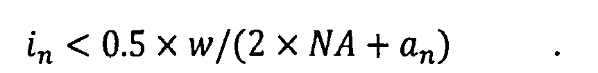
- Das Belichtungsverfahren nach Anspruch 3, wobei der Abstand in zwischen der Maske und der Feldblende folgende Bedingung erfüllt:

Applications Claiming Priority (3)
| Application Number | Priority Date | Filing Date | Title |
|---|---|---|---|
| JP2003003868 | 2003-01-10 | ||
| JP2003003868 | 2003-01-10 | ||
| PCT/JP2004/000129 WO2004064128A1 (ja) | 2003-01-10 | 2004-01-09 | 露光装置および露光方法 |
Publications (3)
| Publication Number | Publication Date |
|---|---|
| EP1585169A1 EP1585169A1 (de) | 2005-10-12 |
| EP1585169A4 EP1585169A4 (de) | 2007-07-18 |
| EP1585169B1 true EP1585169B1 (de) | 2009-11-18 |
Family
ID=32708922
Family Applications (1)
| Application Number | Title | Priority Date | Filing Date |
|---|---|---|---|
| EP04701103A Expired - Lifetime EP1585169B1 (de) | 2003-01-10 | 2004-01-09 | Belichtungssystem und belichtungsverfahren |
Country Status (6)
| Country | Link |
|---|---|
| US (1) | US7023523B2 (de) |
| EP (1) | EP1585169B1 (de) |
| JP (1) | JP4822417B2 (de) |
| AT (1) | ATE449417T1 (de) |
| DE (1) | DE602004024168D1 (de) |
| WO (1) | WO2004064128A1 (de) |
Families Citing this family (5)
| Publication number | Priority date | Publication date | Assignee | Title |
|---|---|---|---|---|
| US7312851B2 (en) * | 2004-06-23 | 2007-12-25 | Nikon Corporation | Projection optical system, exposure apparatus, and exposure method in which a reflective projection optical system has a non-circular aperture stop |
| JP5007538B2 (ja) * | 2006-08-30 | 2012-08-22 | 株式会社ニコン | 露光装置、デバイスの製造方法及び露光方法 |
| DE102008002377A1 (de) | 2007-07-17 | 2009-01-22 | Carl Zeiss Smt Ag | Beleuchtungssystem sowie Projektionsbelichtungsanlage für die Mikrolithografie mit einem derartigen Beleuchtungssystem |
| JP5061063B2 (ja) * | 2008-05-20 | 2012-10-31 | ギガフォトン株式会社 | 極端紫外光用ミラーおよび極端紫外光源装置 |
| KR102160046B1 (ko) * | 2010-04-02 | 2020-09-28 | 가부시키가이샤 니콘 | 조명 광학계, 노광 방법 및 디바이스 제조 방법 |
Family Cites Families (12)
| Publication number | Priority date | Publication date | Assignee | Title |
|---|---|---|---|---|
| US5315629A (en) * | 1990-10-10 | 1994-05-24 | At&T Bell Laboratories | Ringfield lithography |
| US5583609A (en) * | 1993-04-23 | 1996-12-10 | Nikon Corporation | Projection exposure apparatus |
| US5729331A (en) * | 1993-06-30 | 1998-03-17 | Nikon Corporation | Exposure apparatus, optical projection apparatus and a method for adjusting the optical projection apparatus |
| JP3057998B2 (ja) * | 1994-02-16 | 2000-07-04 | キヤノン株式会社 | 照明装置及びそれを用いた投影露光装置 |
| JP3358097B2 (ja) * | 1994-04-12 | 2002-12-16 | 株式会社ニコン | X線投影露光装置 |
| JP3624523B2 (ja) * | 1996-03-06 | 2005-03-02 | 株式会社ニコン | X線投影露光装置 |
| JPH1092727A (ja) * | 1996-09-11 | 1998-04-10 | Canon Inc | 投影露光装置 |
| JP2000091220A (ja) * | 1998-09-08 | 2000-03-31 | Nikon Corp | 投影露光装置及び投影露光方法 |
| JP2000286191A (ja) * | 1999-03-31 | 2000-10-13 | Nikon Corp | 露光装置および露光方法ならびにデバイス製造方法 |
| JP2000349009A (ja) * | 1999-06-04 | 2000-12-15 | Nikon Corp | 露光方法及び装置 |
| JP2000356855A (ja) * | 1999-06-15 | 2000-12-26 | Nikon Corp | 照明領域設定装置および露光装置 |
| JP3363882B2 (ja) * | 2000-10-17 | 2003-01-08 | 株式会社日立製作所 | 露光装置 |
-
2004
- 2004-01-09 DE DE602004024168T patent/DE602004024168D1/de not_active Expired - Lifetime
- 2004-01-09 WO PCT/JP2004/000129 patent/WO2004064128A1/ja not_active Ceased
- 2004-01-09 AT AT04701103T patent/ATE449417T1/de not_active IP Right Cessation
- 2004-01-09 EP EP04701103A patent/EP1585169B1/de not_active Expired - Lifetime
- 2004-01-09 JP JP2005507991A patent/JP4822417B2/ja not_active Expired - Fee Related
-
2005
- 2005-07-07 US US11/177,141 patent/US7023523B2/en not_active Expired - Lifetime
Also Published As
| Publication number | Publication date |
|---|---|
| JP4822417B2 (ja) | 2011-11-24 |
| EP1585169A1 (de) | 2005-10-12 |
| DE602004024168D1 (de) | 2009-12-31 |
| ATE449417T1 (de) | 2009-12-15 |
| US20050264789A1 (en) | 2005-12-01 |
| US7023523B2 (en) | 2006-04-04 |
| EP1585169A4 (de) | 2007-07-18 |
| JPWO2004064128A1 (ja) | 2006-05-18 |
| WO2004064128A1 (ja) | 2004-07-29 |
Similar Documents
| Publication | Publication Date | Title |
|---|---|---|
| JP3862347B2 (ja) | X線縮小露光装置およびこれを利用したデバイス製造方法 | |
| JP3943280B2 (ja) | リソグラフィック投影装置 | |
| KR100583694B1 (ko) | 정렬마크가 제공된 기판, 마스크 설계방법, 컴퓨터프로그램, 상기 마크를 노광하는 마스크, 디바이스제조방법 및 그 디바이스 | |
| EP0678768B1 (de) | Projektionsbelichtungsgerät und Herstellungsverfahren für eine Mikrovorrichtung | |
| US20050243296A1 (en) | Position detecting method and apparatus, exposure apparatus and device manufacturing method | |
| KR100585461B1 (ko) | 마이크로리소그래피 투영장치 | |
| JP3413160B2 (ja) | 照明装置及びそれを用いた走査型露光装置 | |
| JP2003178969A (ja) | リソグラフィ装置およびデバイスの製造方法 | |
| US20080143987A1 (en) | Exposure apparatus and device fabrication method | |
| US9423686B2 (en) | Mask for microlithography and scanning projection exposure method utilizing the mask | |
| US8085384B2 (en) | Exposure apparatus | |
| JP4924421B2 (ja) | センサの校正方法、露光方法、露光装置、デバイス製造方法、および反射型マスク | |
| US7826036B2 (en) | Scanning exposure apparatus and method of manufacturing device | |
| KR101501303B1 (ko) | 조명 광학 장치, 노광 장치, 및 디바이스 제조 방법 | |
| EP1517339A2 (de) | Optisches Beleuchtungssystem und Belichtungsanlage | |
| KR20040090734A (ko) | 리소그래피 장치 및 디바이스 제조방법 | |
| JP2001244183A (ja) | 投影露光装置 | |
| EP1585169B1 (de) | Belichtungssystem und belichtungsverfahren | |
| US6573977B1 (en) | Exposure control method, exposure apparatus and device manufacturing method | |
| KR100563103B1 (ko) | 광학요소를 제조하는 방법, 리소그래피장치 및 디바이스제조방법 | |
| JP2004356291A (ja) | 走査露光装置及び走査露光方法 | |
| JP2000133563A (ja) | 露光方法及び露光装置 | |
| CN121532705A (zh) | 量测设备 | |
| JP2005072513A (ja) | 露光装置および露光方法 | |
| JP2006128366A (ja) | 露光装置、露光方法、およびデバイスの製造方法 |
Legal Events
| Date | Code | Title | Description |
|---|---|---|---|
| PUAI | Public reference made under article 153(3) epc to a published international application that has entered the european phase |
Free format text: ORIGINAL CODE: 0009012 |
|
| 17P | Request for examination filed |
Effective date: 20050707 |
|
| AK | Designated contracting states |
Kind code of ref document: A1 Designated state(s): AT BE BG CH CY CZ DE DK EE ES FI FR GB GR HU IE IT LI LU MC NL PT RO SE SI SK TR |
|
| AX | Request for extension of the european patent |
Extension state: AL LT LV MK |
|
| DAX | Request for extension of the european patent (deleted) | ||
| A4 | Supplementary search report drawn up and despatched |
Effective date: 20070619 |
|
| GRAP | Despatch of communication of intention to grant a patent |
Free format text: ORIGINAL CODE: EPIDOSNIGR1 |
|
| GRAS | Grant fee paid |
Free format text: ORIGINAL CODE: EPIDOSNIGR3 |
|
| GRAA | (expected) grant |
Free format text: ORIGINAL CODE: 0009210 |
|
| AK | Designated contracting states |
Kind code of ref document: B1 Designated state(s): AT BE BG CH CY CZ DE DK EE ES FI FR GB GR HU IE IT LI LU MC NL PT RO SE SI SK TR |
|
| REG | Reference to a national code |
Ref country code: GB Ref legal event code: FG4D |
|
| REG | Reference to a national code |
Ref country code: CH Ref legal event code: EP |
|
| REG | Reference to a national code |
Ref country code: IE Ref legal event code: FG4D |
|
| REF | Corresponds to: |
Ref document number: 602004024168 Country of ref document: DE Date of ref document: 20091231 Kind code of ref document: P |
|
| PG25 | Lapsed in a contracting state [announced via postgrant information from national office to epo] |
Ref country code: SE Free format text: LAPSE BECAUSE OF FAILURE TO SUBMIT A TRANSLATION OF THE DESCRIPTION OR TO PAY THE FEE WITHIN THE PRESCRIBED TIME-LIMIT Effective date: 20091118 Ref country code: FI Free format text: LAPSE BECAUSE OF FAILURE TO SUBMIT A TRANSLATION OF THE DESCRIPTION OR TO PAY THE FEE WITHIN THE PRESCRIBED TIME-LIMIT Effective date: 20091118 Ref country code: ES Free format text: LAPSE BECAUSE OF FAILURE TO SUBMIT A TRANSLATION OF THE DESCRIPTION OR TO PAY THE FEE WITHIN THE PRESCRIBED TIME-LIMIT Effective date: 20100228 Ref country code: PT Free format text: LAPSE BECAUSE OF FAILURE TO SUBMIT A TRANSLATION OF THE DESCRIPTION OR TO PAY THE FEE WITHIN THE PRESCRIBED TIME-LIMIT Effective date: 20100318 |
|
| PG25 | Lapsed in a contracting state [announced via postgrant information from national office to epo] |
Ref country code: SI Free format text: LAPSE BECAUSE OF FAILURE TO SUBMIT A TRANSLATION OF THE DESCRIPTION OR TO PAY THE FEE WITHIN THE PRESCRIBED TIME-LIMIT Effective date: 20091118 Ref country code: CY Free format text: LAPSE BECAUSE OF FAILURE TO SUBMIT A TRANSLATION OF THE DESCRIPTION OR TO PAY THE FEE WITHIN THE PRESCRIBED TIME-LIMIT Effective date: 20091118 |
|
| PG25 | Lapsed in a contracting state [announced via postgrant information from national office to epo] |
Ref country code: AT Free format text: LAPSE BECAUSE OF FAILURE TO SUBMIT A TRANSLATION OF THE DESCRIPTION OR TO PAY THE FEE WITHIN THE PRESCRIBED TIME-LIMIT Effective date: 20091118 Ref country code: BE Free format text: LAPSE BECAUSE OF FAILURE TO SUBMIT A TRANSLATION OF THE DESCRIPTION OR TO PAY THE FEE WITHIN THE PRESCRIBED TIME-LIMIT Effective date: 20091118 |
|
| RAP2 | Party data changed (patent owner data changed or rights of a patent transferred) |
Owner name: NIKON CORPORATION |
|
| PG25 | Lapsed in a contracting state [announced via postgrant information from national office to epo] |
Ref country code: EE Free format text: LAPSE BECAUSE OF FAILURE TO SUBMIT A TRANSLATION OF THE DESCRIPTION OR TO PAY THE FEE WITHIN THE PRESCRIBED TIME-LIMIT Effective date: 20091118 Ref country code: DK Free format text: LAPSE BECAUSE OF FAILURE TO SUBMIT A TRANSLATION OF THE DESCRIPTION OR TO PAY THE FEE WITHIN THE PRESCRIBED TIME-LIMIT Effective date: 20091118 Ref country code: BG Free format text: LAPSE BECAUSE OF FAILURE TO SUBMIT A TRANSLATION OF THE DESCRIPTION OR TO PAY THE FEE WITHIN THE PRESCRIBED TIME-LIMIT Effective date: 20100218 Ref country code: RO Free format text: LAPSE BECAUSE OF FAILURE TO SUBMIT A TRANSLATION OF THE DESCRIPTION OR TO PAY THE FEE WITHIN THE PRESCRIBED TIME-LIMIT Effective date: 20091118 |
|
| PG25 | Lapsed in a contracting state [announced via postgrant information from national office to epo] |
Ref country code: CZ Free format text: LAPSE BECAUSE OF FAILURE TO SUBMIT A TRANSLATION OF THE DESCRIPTION OR TO PAY THE FEE WITHIN THE PRESCRIBED TIME-LIMIT Effective date: 20091118 Ref country code: SK Free format text: LAPSE BECAUSE OF FAILURE TO SUBMIT A TRANSLATION OF THE DESCRIPTION OR TO PAY THE FEE WITHIN THE PRESCRIBED TIME-LIMIT Effective date: 20091118 Ref country code: MC Free format text: LAPSE BECAUSE OF NON-PAYMENT OF DUE FEES Effective date: 20100131 |
|
| REG | Reference to a national code |
Ref country code: CH Ref legal event code: PL |
|
| PLBE | No opposition filed within time limit |
Free format text: ORIGINAL CODE: 0009261 |
|
| STAA | Information on the status of an ep patent application or granted ep patent |
Free format text: STATUS: NO OPPOSITION FILED WITHIN TIME LIMIT |
|
| REG | Reference to a national code |
Ref country code: FR Ref legal event code: ST Effective date: 20100930 |
|
| 26N | No opposition filed |
Effective date: 20100819 |
|
| GBPC | Gb: european patent ceased through non-payment of renewal fee |
Effective date: 20100218 |
|
| PG25 | Lapsed in a contracting state [announced via postgrant information from national office to epo] |
Ref country code: FR Free format text: LAPSE BECAUSE OF NON-PAYMENT OF DUE FEES Effective date: 20100201 Ref country code: GR Free format text: LAPSE BECAUSE OF FAILURE TO SUBMIT A TRANSLATION OF THE DESCRIPTION OR TO PAY THE FEE WITHIN THE PRESCRIBED TIME-LIMIT Effective date: 20100219 Ref country code: LI Free format text: LAPSE BECAUSE OF NON-PAYMENT OF DUE FEES Effective date: 20100131 Ref country code: CH Free format text: LAPSE BECAUSE OF NON-PAYMENT OF DUE FEES Effective date: 20100131 |
|
| PG25 | Lapsed in a contracting state [announced via postgrant information from national office to epo] |
Ref country code: IE Free format text: LAPSE BECAUSE OF NON-PAYMENT OF DUE FEES Effective date: 20100109 |
|
| PG25 | Lapsed in a contracting state [announced via postgrant information from national office to epo] |
Ref country code: GB Free format text: LAPSE BECAUSE OF NON-PAYMENT OF DUE FEES Effective date: 20100218 Ref country code: IT Free format text: LAPSE BECAUSE OF FAILURE TO SUBMIT A TRANSLATION OF THE DESCRIPTION OR TO PAY THE FEE WITHIN THE PRESCRIBED TIME-LIMIT Effective date: 20091118 |
|
| PG25 | Lapsed in a contracting state [announced via postgrant information from national office to epo] |
Ref country code: HU Free format text: LAPSE BECAUSE OF FAILURE TO SUBMIT A TRANSLATION OF THE DESCRIPTION OR TO PAY THE FEE WITHIN THE PRESCRIBED TIME-LIMIT Effective date: 20100519 Ref country code: LU Free format text: LAPSE BECAUSE OF NON-PAYMENT OF DUE FEES Effective date: 20100109 |
|
| PG25 | Lapsed in a contracting state [announced via postgrant information from national office to epo] |
Ref country code: TR Free format text: LAPSE BECAUSE OF FAILURE TO SUBMIT A TRANSLATION OF THE DESCRIPTION OR TO PAY THE FEE WITHIN THE PRESCRIBED TIME-LIMIT Effective date: 20091118 |
|
| PGFP | Annual fee paid to national office [announced via postgrant information from national office to epo] |
Ref country code: NL Payment date: 20211216 Year of fee payment: 19 |
|
| PGFP | Annual fee paid to national office [announced via postgrant information from national office to epo] |
Ref country code: DE Payment date: 20211130 Year of fee payment: 19 |
|
| REG | Reference to a national code |
Ref country code: DE Ref legal event code: R119 Ref document number: 602004024168 Country of ref document: DE |
|
| REG | Reference to a national code |
Ref country code: NL Ref legal event code: MM Effective date: 20230201 |
|
| PG25 | Lapsed in a contracting state [announced via postgrant information from national office to epo] |
Ref country code: NL Free format text: LAPSE BECAUSE OF NON-PAYMENT OF DUE FEES Effective date: 20230201 Ref country code: DE Free format text: LAPSE BECAUSE OF NON-PAYMENT OF DUE FEES Effective date: 20230801 |