EP1582500A2 - Ableitung des Ladugsaufbaus auf einem Teil eines Wafers. - Google Patents
Ableitung des Ladugsaufbaus auf einem Teil eines Wafers. Download PDFInfo
- Publication number
- EP1582500A2 EP1582500A2 EP05251082A EP05251082A EP1582500A2 EP 1582500 A2 EP1582500 A2 EP 1582500A2 EP 05251082 A EP05251082 A EP 05251082A EP 05251082 A EP05251082 A EP 05251082A EP 1582500 A2 EP1582500 A2 EP 1582500A2
- Authority
- EP
- European Patent Office
- Prior art keywords
- conduction layer
- wafer portion
- layer
- etch
- wafer
- Prior art date
- Legal status (The legal status is an assumption and is not a legal conclusion. Google has not performed a legal analysis and makes no representation as to the accuracy of the status listed.)
- Withdrawn
Links
Images

Classifications
-
- H—ELECTRICITY
- H10—SEMICONDUCTOR DEVICES; ELECTRIC SOLID-STATE DEVICES NOT OTHERWISE PROVIDED FOR
- H10P—GENERIC PROCESSES OR APPARATUS FOR THE MANUFACTURE OR TREATMENT OF DEVICES COVERED BY CLASS H10
- H10P50/00—Etching of wafers, substrates or parts of devices
- H10P50/20—Dry etching; Plasma etching; Reactive-ion etching
- H10P50/24—Dry etching; Plasma etching; Reactive-ion etching of semiconductor materials
- H10P50/242—Dry etching; Plasma etching; Reactive-ion etching of semiconductor materials of Group IV materials
- H10P50/244—Dry etching; Plasma etching; Reactive-ion etching of semiconductor materials of Group IV materials comprising alternated and repeated etching and passivation steps
-
- B—PERFORMING OPERATIONS; TRANSPORTING
- B81—MICROSTRUCTURAL TECHNOLOGY
- B81C—PROCESSES OR APPARATUS SPECIALLY ADAPTED FOR THE MANUFACTURE OR TREATMENT OF MICROSTRUCTURAL DEVICES OR SYSTEMS
- B81C1/00—Manufacture or treatment of devices or systems in or on a substrate
- B81C1/00436—Shaping materials, i.e. techniques for structuring the substrate or the layers on the substrate
- B81C1/00555—Achieving a desired geometry, i.e. controlling etch rates, anisotropy or selectivity
- B81C1/00563—Avoid or control over-etching
- B81C1/00579—Avoid charge built-up
Definitions
- the invention relates generally to etching of silicon wafers and m ⁇ re particularly to the elimination of unwanted etched features due to a charge buildup on exposed structures.
- the structure is etched in a wafer.
- the wafer comprises a silicon layer and a backing layer, such as photoresist.
- the etch in one example comprises a Deep Reactive Ion Etch ("DRIE").
- the etch comprises a plasma.
- the plasma in one example contains ions. The ions serve to etch the structure.
- the backing layer is exposed.
- a charge buildup on the structure results from the ions in the etch.
- the charge buildup serves to deflect the ions to one or more sidewalls of the structure.
- the deflection of ions results in an undercutting of the sidewalls and/or a creation of one or more protruding features on the structure.
- vertical, symmetric sidewalls that lack protruding features are desired.
- an exemplary wafer portion 505 comprises a silicon layer 515, a backing layer 520, and a mask layer 525.
- the silicon layer 515 comprises silicon and/or doped silicon.
- the backing layer 520 comprises a photoresist.
- the mask layer 525 in one example comprises silicon dioxide.
- the wafer portion 505 is through-etched during an etch process that etches a structure. 502 within the silicon layer 515.
- the structure 502 comprises sidewalls 525 and 526.
- the backing layer 520 is exposed.
- the backing layer 520 comprises a non-conductive material, (for example, photoresist)
- a charge buildup results in the structures 530 and 531.
- the charge buildup deflects ions from the etch process onto the sidewalls 525 and 526 resulting in etching of the sidewalls 525 and 526.
- the ions produce an undercut 530 in the sidewall 525 and an undercut 531 in the sidewall 526, as will be understood by those skilled in the art.
- the invention in one implementation encompasses an apparatus.
- the apparatus comprises a wafer portion.
- the wafer portion comprises a conduction layer.
- the conduction layer serves to dissipate a portion of a charge buildup on the wafer portion.
- the conduction layer dissipates a portion of a charge buildup on the wafer portion during an etch of the wafer portion.
- an apparatus 100 comprises a wafer portion 105.
- the wafer portion 105 comprises a conduction layer 110, a silicon layer 115, a backing layer 120, and a mask layer 125.
- the conduction layer 110 is electrically coupled with the silicon layer 115.
- the conduction layer 110 is coupled with the backing layer 120.
- the conduction layer 110 comprises a conductive material, such as aluminum or copper.
- a sputtering process in one example is used to apply the conduction layer 110 to the wafer portion 105.
- the conduction layer 110 is applied to the wafer portion 105 from about a thickness sufficient to provide for electrical conductivity and to a thickness as is limited by factors such as coating machinery limits and/or wafer structural limits, as will be appreciated by those skilled in the art.
- the conduction layer 110 is applied to the wafer portion 105 to a thickness in the range of about one half micrometer (" ⁇ m") to about two micrometers.
- the silicon layer 115 in one example comprises a silicon layer, such as silicon or doped silicon.
- the wafer portion 105 undergoes an etch process.
- the etch process comprises a Deep Reactive Ion Etch ("DRIE").
- the etch process comprises a Bosch process.
- the etch process comprises a mixture of reactive species and byproducts of a plasma dissociation process.
- the mixture of reactive species and byproducts of the plasma dissociation process partially comprises ions.
- the ions of the etch process serve to etch a structure, for example, a structure 202, in the silicon layer 115, as will be understood by those skilled in the art.
- the structure 202 in one example comprises one or more sidewalls 205 and/or 210.
- the backing layer 120 comprises a thick resist, for example, Shipley STR1045 photoresist, or an organic material.
- the backing layer 120 is deposited and/or spun onto the wafer portion 105.
- the backing layer 120 comprises a thickness in the range of about four micrometers to about 10 micrometers.
- the backing layer 120 provides structural integrity to the wafer portion 105 and to the structure 202 etched in the wafer portion 105.
- the backing layer 120 also insulates the conduction layer 110 and prevents the conduction layer 110 from becoming part of an undesirable charging path, as will be appreciated by those skilled in the art.
- the backing layer 120 is removed from the wafer portion 105 after completion of the etch process. In another example, the backing layer 120 remains part of the wafer portion 105 after completion of the etch process.
- the mask layer 125 comprises an inorganic material which serves as an etch mask.
- the mask layer 125 is patterned through a combination of lithographic steps for example: deposition of a resist, pattern exposure/development, oxide etch, and resist removal.
- the mask layer 125 comprises a photoresist.
- a pattern is formed in the photoresist in one example through a deposition of a resist, a pattern exposure, and a development of the pattern.
- the pattern in the mask layer 125 determines one or more structures, for example, the structure 202, etched in the silicon layer 115, as will be understood by those skilled in the art.
- the conduction layer 110 in one example, promotes a reduction in an undercutting of the structure 202 etched in the wafer portion 105. by dissipating a portion of a charge buildup on the wafer portion 105 through exposure of the conduction layer 110 during an etch of the wafer portion 105.
- the wafer portion 105 undergoes the etch process, for example, a single-sided etch process.
- the conduction layer 110 is exposed within the structure 202.
- the conduction layer 110 electrically couples the sidewalls 205 and 210.
- the sidewalls 205 and 210 comprise respective electrostatic potentials.
- the respective electrostatic potentials of the sidewalls 205 and 210 comprise electrostatic potentials substantially similar to an electrostatic potential of the conduction layer 110.
- a charge buildup occurs on the wafer portion 105.
- a portion of the charge buildup on the wafer portion 105 is dissipated.
- a portion of the charge buildup on the wafer portion 105 is dissipated through employment of one or more of the sidewalls 205 and 210 of the wafer portion 105 and the conductive layer 110.
- the conduction layer 110 prevents ions from deflecting onto the sidewalls 205 and 210 of the structure 202, as will be appreciated by those skilled in the art.
- the conduction layer 110 mitigates the effects of etch rate variation across the wafer portion 105, as will be appreciated by those skilled in the art.
- the wafer portion 105 comprises a plurality of structures 202.
- a first structure 202 comprises a first etch rate and a second structure 202 comprises a second etch rate.
- the first etch rate differs from the second etch rate, as will be understood by those skilled in the art.
- the wafer portion 105 undergoes the etch process for a period of time.
- the period of time comprises a period of time to accommodate each of the etch rates associated with the first structure 202 and the second structure 202. For example, where the first etch rate is greater than the second etch rate, the period of time comprises the period of time to fully-etch the second structure 202.
- the conduction layer 110 Upon exposure of the conduction layer 110 within the first structure 202, the conduction layer 110 promotes the reduction of the undercutting.
- the conduction layer 110 allows the wafer portion 105 to be etched for the period of time to fully-etch the second structure 202 without degrading features of the first structure 202, as will be appreciated by those skilled in the art.
- FIGS. 1-2 an illustrative description of exemplary operation of the apparatus 100 is now presented, for explanatory purposes.
- the wafer portion 105 undergoes the etch process on the first side 130 to the point just before the through-etch.
- the second side 135 of the wafer portion 105 is cleaned.
- the conduction layer 110 for example, aluminum, is applied to the second side 135 of the wafer portion 105 using a sputtering technique.
- the backing layer 120 for example, photoresist, is spun or deposited onto the conduction layer 110.
- the structure 202 of the wafer portion 105 is through-etched during the etch process. The etch process creates the sidewalls 205 and 210 in the wafer portion 105.
- the etch process of the structure 202 exposes the conduction layer 110.
- the conduction layer 110 Upon exposure of the conduction layer 110, the conduction layer 110 dissipates the portion of the charge buildup on the structure 202.
- the conduction layer 110 and the side walls 205 and 210 are at substantially a similar potential and result in the dissipation of the portion of charge buildup on the structure 202.
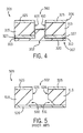
- a wafer portion 305 comprises a conduction layer 310, a silicon layer 315, a backing layer 320, a first oxide layer 325, and a second oxide layer 327.
- the wafer portion 305 undergoes a first portion of an etch process on a first side 306 of the wafer portion 305.
- the wafer portion 305 undergoes the first portion of the etch process up to a point just short of the midpoint of thickness, as will be understood by those skilled in the art.
- the wafer portion 305 undergoes the first portion of the etch process to etch the structure 360 in the silicon layer 315.
- the wafer portion 305 undergoes a second portion of the etch process on a second side 307 of the wafer portion 305.
- the oxide layer 327 is patterned to define a structure 302 to be etched in the second side 307 of the wafer portion 305.
- the second portion of the etch process serves to etch the structure 302 in the silicon layer 115.
- the conduction layer 310 is applied to the second side 307 of the wafer portion 302.
- the conduction layer 310 is coupled with the silicon layer 315.
- the backing layer 320 is applied to the second side 307 of the wafer portion 305.
- the backing layer 320 is coupled with the conductive layer 310.
- the wafer portion 305 undergoes a third portion of the etch process on the first side 306 of the wafer portion 305.
- the third portion of the etch process serves to through-etch the structure 360 in the silicon layer 315.
- the conduction layer 310 is exposed.
- the third portion of the etch process etches the sidewalls 405 and 410 of the structure 360.
- the conduction layer 310 promotes the reduction of the undercutting of the structure 360 etched in the wafer portion 305 and promotes the reduction in the amount of protruding features created on the structure 360.
- the conduction layer 310 dissipates the charge buildup on the structure 360.
- the conduction layer 310 electrically couples the sidewalls 405 and 410.
- the sidewall 405 and 410 and the conduction layer 310 are at substantially a similar potential resulting in the dissipation of the charge buildup on the structure 360.
- the apparatus described herein is one example that comprises a plurality of components such as hardware components. A number of such components can be combined or divided in the apparatus 100.
- the apparatus 100 in one example comprises any (e.g., horizontal, oblique, or vertical) orientation, with the description and figures herein illustrating one exemplary orientation of the apparatus 100, for explanatory purposes.
- the steps or operations described herein are just exemplary. There may be many variations to these steps or operations without departing from the spirit of the invention. For instance, the steps may be performed in a differing order, or steps may be added, deleted, or modified.
Landscapes
- Engineering & Computer Science (AREA)
- Physics & Mathematics (AREA)
- Geometry (AREA)
- Manufacturing & Machinery (AREA)
- Microelectronics & Electronic Packaging (AREA)
- Internal Circuitry In Semiconductor Integrated Circuit Devices (AREA)
- Micromachines (AREA)
Applications Claiming Priority (2)
| Application Number | Priority Date | Filing Date | Title |
|---|---|---|---|
| US10/811,512 US7038293B2 (en) | 2004-03-29 | 2004-03-29 | Dissipation of a charge buildup on a wafer portion |
| US811512 | 2004-03-29 |
Publications (2)
| Publication Number | Publication Date |
|---|---|
| EP1582500A2 true EP1582500A2 (de) | 2005-10-05 |
| EP1582500A3 EP1582500A3 (de) | 2006-04-19 |
Family
ID=34887669
Family Applications (1)
| Application Number | Title | Priority Date | Filing Date |
|---|---|---|---|
| EP05251082A Withdrawn EP1582500A3 (de) | 2004-03-29 | 2005-02-24 | Ableitung des Ladugsaufbaus auf einem Teil eines Wafers. |
Country Status (4)
| Country | Link |
|---|---|
| US (1) | US7038293B2 (de) |
| EP (1) | EP1582500A3 (de) |
| JP (1) | JP2005279923A (de) |
| CA (1) | CA2497933A1 (de) |
Families Citing this family (3)
| Publication number | Priority date | Publication date | Assignee | Title |
|---|---|---|---|---|
| JP4479577B2 (ja) * | 2005-04-28 | 2010-06-09 | 株式会社日立製作所 | 半導体装置 |
| US8753974B2 (en) * | 2007-06-20 | 2014-06-17 | Micron Technology, Inc. | Charge dissipation of cavities |
| JP5849398B2 (ja) * | 2011-02-01 | 2016-01-27 | 株式会社豊田中央研究所 | Memsデバイスの製造方法およびmemsデバイス |
Family Cites Families (11)
| Publication number | Priority date | Publication date | Assignee | Title |
|---|---|---|---|---|
| JPS6432632A (en) * | 1987-07-29 | 1989-02-02 | Hitachi Ltd | Manufacture of semiconductor device |
| US5129981A (en) | 1991-03-14 | 1992-07-14 | General Motors Corporation | Method of selectively etching silicon |
| JPH06151387A (ja) * | 1992-11-10 | 1994-05-31 | Nippon Telegr & Teleph Corp <Ntt> | シリコンの精密加工方法 |
| JPH06291031A (ja) * | 1993-03-30 | 1994-10-18 | Masamichi Fujihira | 微細加工方法及びこの方法で加工された加工物 |
| JP3112395B2 (ja) * | 1995-06-22 | 2000-11-27 | シャープ株式会社 | ドライエッチング装置およびドライエッチング方法 |
| US5865938A (en) * | 1996-06-25 | 1999-02-02 | Xerox Corporation | Wafer chuck for inducing an electrical bias across wafer heterojunctions |
| AUPO281896A0 (en) | 1996-10-04 | 1996-10-31 | Unisearch Limited | Reactive ion etching of silica structures for integrated optics applications |
| DE19907621B4 (de) * | 1999-02-23 | 2005-12-15 | Robert Bosch Gmbh | Ätzmaskierung |
| JP3990076B2 (ja) | 1999-06-30 | 2007-10-10 | 株式会社東芝 | 半導体装置の製造方法 |
| US6613666B2 (en) * | 2001-12-07 | 2003-09-02 | Applied Materials Inc. | Method of reducing plasma charging damage during dielectric etch process for dual damascene interconnect structures |
| US6905626B2 (en) * | 2002-07-24 | 2005-06-14 | Unaxis Usa Inc. | Notch-free etching of high aspect SOI structures using alternating deposition and etching and pulsed plasma |
-
2004
- 2004-03-29 US US10/811,512 patent/US7038293B2/en not_active Expired - Fee Related
-
2005
- 2005-02-22 CA CA002497933A patent/CA2497933A1/en not_active Abandoned
- 2005-02-24 EP EP05251082A patent/EP1582500A3/de not_active Withdrawn
- 2005-03-29 JP JP2005093383A patent/JP2005279923A/ja active Pending
Also Published As
| Publication number | Publication date |
|---|---|
| JP2005279923A (ja) | 2005-10-13 |
| CA2497933A1 (en) | 2005-09-29 |
| US7038293B2 (en) | 2006-05-02 |
| US20050212077A1 (en) | 2005-09-29 |
| EP1582500A3 (de) | 2006-04-19 |
Similar Documents
| Publication | Publication Date | Title |
|---|---|---|
| CN101740357B (zh) | 在半导体器件中形成微图案的方法 | |
| US6752931B2 (en) | Method for using DRIE with reduced lateral etching | |
| JP7809705B2 (ja) | 静電クランプ | |
| JP4220229B2 (ja) | 荷電粒子線露光用マスクブランクスおよび荷電粒子線露光用マスクの製造方法 | |
| US7629263B2 (en) | Semiconductor sensor production method and semiconductor sensor | |
| US7038293B2 (en) | Dissipation of a charge buildup on a wafer portion | |
| US11990344B2 (en) | Low-cost method of making a hard mask for high resolution and low dimensional variations for the fabrication and manufacturing of micro- and nano-devices and -systems | |
| EP0540261B1 (de) | Verfahren zur Entfernung von Polymeren aus Sacklöchern in Halbleitervorrichtungen | |
| US20020122993A1 (en) | Stencil reticles for charged-particle-beam microlithography, and fabrication methods for making same | |
| JPH0471334B2 (de) | ||
| US20130224958A1 (en) | Through hole forming method | |
| US20020028394A1 (en) | Method for manufacturing a membrane mask | |
| KR100796509B1 (ko) | 반도체 소자의 제조방법 | |
| US20020139770A1 (en) | Methods for fabricating segmented reticle blanks having uniformly machined grillage, and reticle blanks and reticles formed thereby | |
| KR100672173B1 (ko) | 반도체 소자의 하드 마스크 패턴 형성 방법 | |
| CN112466803B (zh) | 半导体器件的制作方法 | |
| JP4969776B2 (ja) | 水晶デバイスの製造方法 | |
| JPH0555218A (ja) | 半導体装置及びその製造方法 | |
| KR20100042423A (ko) | 반도체 소자의 패턴 형성 방법 | |
| JPH10209166A (ja) | 半導体装置の製造方法 | |
| KR100516771B1 (ko) | 반도체 소자의 게이트 전극 형성방법 | |
| KR100898589B1 (ko) | 반도체 소자 제조 방법 | |
| KR100192374B1 (ko) | 반도체 소자 식각 방법 | |
| JPH02224240A (ja) | パターン形成方法 | |
| JPH1079392A (ja) | 半導体装置の配線層の製造方法 |
Legal Events
| Date | Code | Title | Description |
|---|---|---|---|
| PUAI | Public reference made under article 153(3) epc to a published international application that has entered the european phase |
Free format text: ORIGINAL CODE: 0009012 |
|
| AK | Designated contracting states |
Kind code of ref document: A2 Designated state(s): AT BE BG CH CY CZ DE DK EE ES FI FR GB GR HU IE IS IT LI LT LU MC NL PL PT RO SE SI SK TR |
|
| AX | Request for extension of the european patent |
Extension state: AL BA HR LV MK YU |
|
| PUAL | Search report despatched |
Free format text: ORIGINAL CODE: 0009013 |
|
| AK | Designated contracting states |
Kind code of ref document: A3 Designated state(s): AT BE BG CH CY CZ DE DK EE ES FI FR GB GR HU IE IS IT LI LT LU MC NL PL PT RO SE SI SK TR |
|
| AX | Request for extension of the european patent |
Extension state: AL BA HR LV MK YU |
|
| 17P | Request for examination filed |
Effective date: 20060919 |
|
| 17Q | First examination report despatched |
Effective date: 20061115 |
|
| AKX | Designation fees paid |
Designated state(s): DE FR GB IT |
|
| STAA | Information on the status of an ep patent application or granted ep patent |
Free format text: STATUS: THE APPLICATION IS DEEMED TO BE WITHDRAWN |
|
| 18D | Application deemed to be withdrawn |
Effective date: 20090827 |