EP1582003B1 - Mehrmode-empfänger - Google Patents
Mehrmode-empfänger Download PDFInfo
- Publication number
- EP1582003B1 EP1582003B1 EP03777110A EP03777110A EP1582003B1 EP 1582003 B1 EP1582003 B1 EP 1582003B1 EP 03777110 A EP03777110 A EP 03777110A EP 03777110 A EP03777110 A EP 03777110A EP 1582003 B1 EP1582003 B1 EP 1582003B1
- Authority
- EP
- European Patent Office
- Prior art keywords
- seq
- received signal
- receiver
- spread
- signal
- Prior art date
- Legal status (The legal status is an assumption and is not a legal conclusion. Google has not performed a legal analysis and makes no representation as to the accuracy of the status listed.)
- Expired - Lifetime
Links
- 230000007480 spreading Effects 0.000 claims abstract description 47
- 238000001914 filtration Methods 0.000 claims abstract description 18
- 238000001228 spectrum Methods 0.000 claims description 24
- 238000000034 method Methods 0.000 claims description 19
- 101001047783 Homo sapiens Histone PARylation factor 1 Proteins 0.000 claims description 10
- 101000964789 Homo sapiens Zinc finger protein 83 Proteins 0.000 claims description 10
- 230000010354 integration Effects 0.000 claims description 8
- 102100024348 Beta-adducin Human genes 0.000 claims description 5
- 101000689619 Homo sapiens Beta-adducin Proteins 0.000 claims description 5
- 102100024023 Histone PARylation factor 1 Human genes 0.000 claims 2
- 230000008569 process Effects 0.000 description 9
- 102100040639 Zinc finger protein 83 Human genes 0.000 description 8
- 230000008901 benefit Effects 0.000 description 5
- 102100034033 Alpha-adducin Human genes 0.000 description 4
- PEDCQBHIVMGVHV-UHFFFAOYSA-N Glycerine Chemical compound OCC(O)CO PEDCQBHIVMGVHV-UHFFFAOYSA-N 0.000 description 4
- 101000799076 Homo sapiens Alpha-adducin Proteins 0.000 description 4
- 101000629598 Rattus norvegicus Sterol regulatory element-binding protein 1 Proteins 0.000 description 4
- 230000005540 biological transmission Effects 0.000 description 3
- 239000013078 crystal Substances 0.000 description 3
- 238000005070 sampling Methods 0.000 description 3
- 230000003595 spectral effect Effects 0.000 description 3
- RTZKZFJDLAIYFH-UHFFFAOYSA-N Diethyl ether Chemical compound CCOCC RTZKZFJDLAIYFH-UHFFFAOYSA-N 0.000 description 2
- 238000006243 chemical reaction Methods 0.000 description 2
- 230000007423 decrease Effects 0.000 description 2
- 230000000694 effects Effects 0.000 description 2
- 230000001747 exhibiting effect Effects 0.000 description 2
- 230000009467 reduction Effects 0.000 description 2
- 230000001360 synchronised effect Effects 0.000 description 2
- 102100036601 Aggrecan core protein Human genes 0.000 description 1
- 108091006419 SLC25A12 Proteins 0.000 description 1
- 239000003990 capacitor Substances 0.000 description 1
- 239000000969 carrier Substances 0.000 description 1
- 238000004891 communication Methods 0.000 description 1
- 230000021615 conjugation Effects 0.000 description 1
- 238000010276 construction Methods 0.000 description 1
- 230000006378 damage Effects 0.000 description 1
- 230000001934 delay Effects 0.000 description 1
- 238000010586 diagram Methods 0.000 description 1
- 238000005562 fading Methods 0.000 description 1
- PCHJSUWPFVWCPO-UHFFFAOYSA-N gold Chemical compound [Au] PCHJSUWPFVWCPO-UHFFFAOYSA-N 0.000 description 1
- 239000010931 gold Substances 0.000 description 1
- 229910052737 gold Inorganic materials 0.000 description 1
- 238000002955 isolation Methods 0.000 description 1
- 238000012986 modification Methods 0.000 description 1
- 230000004048 modification Effects 0.000 description 1
- 244000045947 parasite Species 0.000 description 1
Images


Classifications
-
- H—ELECTRICITY
- H04—ELECTRIC COMMUNICATION TECHNIQUE
- H04J—MULTIPLEX COMMUNICATION
- H04J13/00—Code division multiplex systems
- H04J13/0003—Code application, i.e. aspects relating to how codes are applied to form multiplexed channels
-
- H—ELECTRICITY
- H04—ELECTRIC COMMUNICATION TECHNIQUE
- H04B—TRANSMISSION
- H04B1/00—Details of transmission systems, not covered by a single one of groups H04B3/00 - H04B13/00; Details of transmission systems not characterised by the medium used for transmission
- H04B1/69—Spread spectrum techniques
- H04B1/707—Spread spectrum techniques using direct sequence modulation
-
- H—ELECTRICITY
- H04—ELECTRIC COMMUNICATION TECHNIQUE
- H04J—MULTIPLEX COMMUNICATION
- H04J13/00—Code division multiplex systems
- H04J13/0007—Code type
- H04J13/0022—PN, e.g. Kronecker
Definitions
- the present invention relates to a receiver for processing a received signal, said receiver being multimode.
- the invention further relates to an associated method for receiving a signal in any mode.
- Such a receiver may be used in particular in any multimode terminals such as a mobile phone using multimode standards like GSM and W-CDMA (UMTS).
- multimode standards like GSM and W-CDMA (UMTS).
- a multimode terminal comprises a receiver, which permits to manage the received signal, whatever the standard of this signal is.
- the emerging multimode receivers in a terminal are implemented by using as many RF chipsets as there are targeted standards by the terminal.
- the latest triple band mobile phone GSM/DCS/PCS which also includes bluetooth standard and FM radio reception, is implemented with three separate chipsets, one for each standard as described in the RFMD UMTS/DCS/GSM chipset document for their RF51176 receiver, for example.
- WO 02 101 945 shows a multimode receiver for GSM, DCS, PCS and UMTS.
- the receiver comprises:
- the method for receiving a signal comprises the steps of:
- such a receiver makes it possible to have only one chip, i.e., one reception chain for all the standards used for transmission, such as GSM or W-CDMA also called UMTS thanks to the spreading of the received signal.
- the receiver is characterized in that the spreading section is adapted to produce a spread spectrum oscillator and a spreading sequence, in order to expand the bandwidth of a received signal.
- the receiver is characterized in that the spreading section further comprises unique rejection means for all the modes for suppressing the adjacent carrier frequencies of the associated received signals.
- the receiver is characterized in that the channel filtering section is common for all the modes.
- the receiver is characterized in that the channel filtering section comprises:
- the receiver is characterized in that the channel filtering section further comprises adding means for redirecting a spread received signal coming from a block of low-noise amplifier and associated mixers to the first rejection means.
- the receiver is characterized in that the baseband chip further comprises:
- the receiver is characterized in that the despreading means comprise:
- the receiver is characterized in that the baseband chip further comprises synchronization means for synchronizing a spread signal with a corresponding despreading sequence.
- the method is characterized in that it comprises also a step of producing a spread spectrum oscillator and a spreading sequence in order to expand the bandwidth of the received signal.
- the present invention relates to a receiver REC for processing a received signal.
- Said receiver REC is used in particular in communication systems and more particularly in a user equipment such as a mobile phone.
- the receiver comprises a reception chain RX_CHAIN allowing multimode reception, i.e. reception of signals coming from a UMTS base station or a GSM base station for example, and in particular in compressed mode operation. In a compressed mode operation, the receiver does not have to "listen” (i.e. synchronize, demodulate and downconvert) simultaneously to two different signals of two different modes GSM and UMTS for example.
- Such a receiver REC is illustrated in Fig.1 .
- the receiver REC comprises:
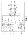
- the channel filtering section CH_SEC is illustrated in Fig.2 .
- the channel filtering section CH_SEC further comprises an adder ADD for adding all received signals SEQ from the amplifier-mixer blocks and output a result directed on the first rejection means HPF1.
- the spreading section SPREAD_SEC is illustrated in Fig.3 .
- the spreading section SPREAD_SEC further comprises further rejection means LPF3 for suppressing the adjacent carrier frequencies of a received signal SEQ, said further means being a low-pass filter.
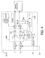
- the baseband chip BB is illustrated in Fig.4 .
- the despreading means DSPR comprise:
- the baseband chip BB_INT further comprises:
- a GSM signal a UMTS signal and a Bluetooth signal will be taken as examples.
- a signal SEQ When receiving a signal SEQ from a base station via the antenna of the User Equipment, i.e. the mobile phone, said signal is received at a certain radio carrier frequency, and with a 3dB bandwidth of 270 kHz for the GSM standard, or with a 3dB bandwidth of around 5MHz for the UMTS standard.
- the signal SEQ is first processed in the mobile phone via the receiver REC. More particularly, in said receiver REC, there is a need to translate this radio frequency to the baseband frequency (0Hz) in order to be able to demodulate the signal so that it can be treated by some other components of the mobile phone further on, such as the loudspeakers.
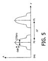
- a GSM signal is illustrated in Fig.5 in the frequency domain.
- Said signal SEQ is centered on the GSM carrier center frequency of F0.
- the center frequency F1 of such an adjacent carrier frequency is also illustrated.
- the difference ⁇ F between the 2 centers F0 and F1 is within the GSM frequency band (900MHz band for example).
- the receiver REC processes a received signal SEQ as follows.
- the receiver REC is multimode.
- Said amplifier LNA allows a decrease of the noise of the corresponding received signal SEQ within the receiver REC.
- a first step 1) if the received signal SEQ is not already spread, for example a GSM or Bluetooth received signal, spreading of the carrier frequency spectrum of said received signal SEQ with a corresponding spreading sequence PN is achieved by the spreading section SPREAD_SEC and the channel filtering section CH_SEC.
- This spreading consists in expanding the bandwidth of the carrier frequency of the signal SEQ by multiplying the data bits of said signal SEQ by a spread spectrum LO.
- Spreading a continuous-wave local oscillator LO via an analog multiplier M0 with the corresponding spreading sequence PN as shown in Fig.3 generates the associated spread-spectrum local oscillator LO.
- the spectrum of a PN sequence is infinite and has a cut-off frequency of 3,84 MHz for the GSM standard and of 1MHz for the Bluetooth standard.
- the local oscillator are spread only in the case of receiving narrowband carriers.
- a 2-wideband CDMA carrier i.e. a UMTS received signal is simpler since the carrier is already a spread spectrum signal. No spreading is achieved for such a signal as can be seen in Fig.3 and the local oscillator LO2 is a simple sine wave, as used in a conventional RF receiver chain (no multiplier M0 is associated to the local oscillator LO2).
- a sequence generator PN_SEQ_GEN generates the corresponding spreading sequence PN at a frequency FN of 3.84 MChip/sec via a clock CHIP-RATE-CLK for any modes except the UMTS one. Said clock permits to have an integer multiple of the desired frequency FN.
- sequence generators PN_SEQ_GEN oversample its output signal to 4, which has the effect of having a frequency of 15.36 MHz.
- the series of multiplexers in the spreading means SPREAD_SEC direct the right spreading sequence PN on the channel section CH_SEC and on the baseband chip BB_INT.
- a spreading sequence PN can be a Gold or Kasami code family well known to those skilled in the art or any other type, such as Walsh codes.
- the different spreading sequences PN associated to the different received signals of the different targeted modes are orthogonal.
- the radio frequency RF chip comprises further rejection means LPF3 which are a low pass filter with a roll-off factor ⁇ of 0.22, which is set at the output of the set of the sequence generator PN_SEQ_GEN.
- This filter LPF3 permits to suppress the adjacent carrier frequencies of a received signal SEQ, and especially those, which are far from the wanted carrier frequency F0.
- Such received signal SEQ is then now exhibiting a root raised cosine RRC spectral occupancy of 3dB bandwidth equal to 2.3 MHz as shown in Fig.6 for any mode except for the UMTS one.
- the occupied bandwidth is identical to that of a FDD-WCDMA carrier (UMTS signal).
- the spread signal SEQ of any mode occupies the bandwidth of the spreading sequence PN of 3.84 Mchip/s in the frequency domain.
- a spread GSM signal can be seen on the Fig.8 .
- the signal SEQ is now exhibiting a spectral occupancy of a typical square wave signal clocked at 3.84 MHz, i.e. sin(x)/x amplitude envelope, with zero crossing at N*3.84 MHz, N being an integer.
- the main carrier frequency F0 has been down-converted to baseband, i.e. centered around 0 Hz.
- mixers M1 & M2 one performs simultaneous spreading of the received signal SEQ via the multiplication by the PN spreading sequence, except for a UMTS signal, and a down-conversion for all the modes to baseband via the multiplication of a spread-spectrum local oscillator LO or a normal-spectrum local oscillator LO2 for the UMTS mode.
- the received signal SEQ is split into 2 components I and Q, well known to the person skilled in the art, via the two quadrature mixers M1 and M2, and that all the following steps are done on the 2 components in parallel. But for the sake of simplification, the term signal SEQ will be used instead of I and Q components.
- This SAW filter cannot be integrated in the RF chip.
- DC rejection is performed as follows.
- the receiver according to the invention saves costs and complexity by ensuring only one channel filtering section CH_SEC is reused to receive any mobile telecommunication standards, as opposed to having several receive chains in parallel.
- a second step 2 Before rejection of DC offset, in a second step 2) , there is a reduction of the noise factor for each component I&Q of a signal SEQ via a fixed gain amplifier AGCF.
- Said gain amplifier AGCF permits to adapt the impedances between the multipliers M1&M2 and the following adders ADD1&ADD2.
- a summing of all the spread received signal is performed via the adders ADD1&ADD2.
- the first adder ADD1 sums all the I components of all the received signals SEQ together
- the second adder ADD2 sums all the Q components of all the received signals SEQ together.
- the adders ADD1&ADD2 have the same function as a multiplexer that directs the IS and QS components on the following stages LPF1-AGC and HPF1.
- a fourth step 4) rejection of the DC offset that remains on said spread carrier frequency spectrums is achieved via a simple DC compensation loop which behaves like a second order high pass filter of programmable high pass cut-off frequency.
- This high pass filters HPF1 (one for each component IS and QS of a signal SEQS) are cascaded with channel filters LPF1, which in this application are used solely to remove any spurs or far adjacent carrier frequencies which would be present despite the use of the sharp low-pass filter LPF3.
- the channel filters LPF1 can be a 5 th order Legendre low-pass filter and have a 3dB cut-off frequency of 2.2 MHz.
- DC offset has two main origins.
- the first one is the self-mixing between the local oscillator LO and self-mixing of RF carrier frequency resulting from either LO or RF leakage at the front-end: DC is generated by the mixing of LO with itself, and the RF signal with itself. This is due to the limited amount of isolation between the LO and RF port inherent in an RF IC.
- the second one is due to second-order intermodulation performance of the receiver, which generates undesirable spectral components at baseband and a strong DC component. This is due in particular to the mixers of the receiver, which are not linear and which introduce input intersection point of 2 nd order known as IIP2 phenomenon.
- both the low frequency cut-off and the high frequency cut-off are adjustable by programming.
- the resulting 3dB bandwidth can vary from 1.9 to 2.2 MHz depending on the cut-off frequency of the analog filters HPF1 implemented in the RF chip.
- this DC offset rejection has the advantage to be easy to implement. No complex components are needed. Moreover, only one DC compensation loop is needed for all the targeted loop, contrary to the state of the art, where there is a need of as many DC compensation loops as there are targeted modes.
- the spreading section SPREAD_SEC has the advantage to allow a good reconstruction of the received signal after DC offset rejection, contrary to a usual DC offset loop compensation.
- a DC offset loop compensation a simple filter with a resistance and a capacitor
- a fifth step 5 once the DC offset has been rejected via HPF1 means, ADC sampling is performed.
- the I and Q-components of a spread signal SEQ require an adequate analog-to-digital converter ADC to sample the 2.2MHz wide (3dB bandwidth) analog signal SEQ in any mode. Sampling is performed with a 4xchip rate clock.
- a sixth step 6 after ADC sampling, there is a despreading of the spread signals SEQ in order to recover the initial received signals SEQ.
- This despreading is achieved in the baseband chip BB_INT of Fig.4 by means of the despreading means DSPR
- the spread section SPREAD_SEC as described above can send the despreading sequence PN used. Since the incoming signal is no longer a binary stream, but an analog waveform, this sequence PN must be acquired by the baseband chip BB_INT via an additional analog-to-digital converter ADC_PN.
- the PN code used for spreading within the RF chip can be filtered with a low-pass filter stage identical to that used in the channel filtering section.
- the despreading process consists in a measure of similarity between the spread signal SEQ and the despreading sequence PN.
- the correlator of the despreading means DSPR permits such a measure. This measure is performed by multiplying the signal and the sequence and summing (integration) the results over a defined time window, here over a bit period. The summing is done after a data decision on the multiplication results leading to a value of, for example, -1, +1.
- despreading sequence PN is split and applied to one multiplier for each I&Q components of the signal SEQ, as shown in Fig.4 .
- time propagation of the spread signal SEQ when it is transmitted from the spreading section to the despreading section said time propagation usually varying from one RF chip to a Baseband chip, depending on the components used between those two parts, especially depending on the low-pass filters.
- a synchronization between the despreading sequence PN and the spread signal SEQ via synchronization means SYNC is performed.
- the synchronization means SYNC comprise a digital delay line DELAY producing a sliding clock S_CLK at 15,36 MHz, and a threshold value TH.
- the despreading sequence PN is fed through the digital delay line DELAY clocked at 4*the chip rate via the clock S_CLK, which results in a 1 ⁇ 4 chip delay resolution.
- the despreading sequence PN can then be shifted in 1 ⁇ 4 chip steps.
- the shifting, i.e. the despreading sequence PN phase is incremented by 1 ⁇ 4 chip, is applied until the despreading sequence PN is synchronized or time-aligned or in phase with the spread signal SEQ, i.e. an optimum correlation peak is obtained.
- the maximum number of shifts is equal to the length LGH of the despreading sequence PN.
- the correlation process is performed via the integration and dump means I&D to reconstruct the received signal SEQ in baseband.
- the sequence PN is shifted from 1 ⁇ 4 chip and the correlation process described above is performed again and so on until an optimum peak is obtained.
- the despreading sequence PN is then fed through the matching filter IIR, as shown in Fig. 4 .
- the despreading sequence PN suffers exactly the same amount of amplitude and phase distortion as the spread signal SEQ, which is necessary to have a good matching of the spread signal and the despreading sequence.
- the correlation product is optimal and ensures an optimal signal-to-noise ratio SNR.
- the synchronization described above has the advantage of having a well-known time propagation or delay of the spread signal SEQ and is unlikely to vary in time since the signal path consists of electrical transmission lines through a cascade of AGC amplifiers and low-pass filters in the RF chip and Baseband chip. Therefore, the architecture of the receiver according to the invention as described above, is obviously advantageous compared to a solution where the spreading section would be in the base station and the despreading section in the mobile phone.
- the first one is a digital despreading within the baseband chip BB_INT as stated above and the second one is an analog despreading in the RF chip.
- the rejection of the adjacent carrier frequencies of a signal SEQ is done via the integration and dump means I&D, and the despreading means must comprise a gain amplifier at the output of the filter IIR in order to adjust the amplitude of the despreading sequence PN with the power of the signal received from the mixers M1 and M2.
- the despreading means must comprise a gain amplifier at the output of the filter IIR in order to adjust the amplitude of the despreading sequence PN with the power of the signal received from the mixers M1 and M2.
- a seventh step 7 after the correlation process, further rejection is achieved via the channel coefficient bank FIR associated to each targeted mode for rejecting adjacent carrier frequencies that could remain on the spectrum of the despread signal SEQ and which are close to the carrier frequency F0.
- a series of multiplexers applies the right coefficient to the associated low-pass filter BB_LPF.
- the coefficient is the cut-off frequency of 130kHz
- the coefficient is the cut-off frequency of 300kHz
- the result of the despreading is that the bandwidth of a received signal SEQ has been compressed from 3.84 Mchip/sec to 135 kHz for a GSM signal.
- the initial received signal SEQ is recovered as shown in Fig. 10 for a GSM signal.
- the resulting I&Q components can then be passed over to the rest of the receiver chain RX_CHAIN to achieve in particular:
- the receiver according to the invention has the advantage of resolving the problems of DC offset loop compensation on narrowband signals by using techniques used for wideband signals leading to a simple solution with low power consumption.
- the receiver according to the invention minimizes the duplication of RF blocks and allows multimode reception to be integrated into a single chip with no complex components.
- Said hardware or software items can be implemented in several manners, such as by means of wired electronic circuits or by means of an integrated circuit that is suitably programmed, respectively.
Landscapes
- Engineering & Computer Science (AREA)
- Computer Networks & Wireless Communication (AREA)
- Signal Processing (AREA)
- Circuits Of Receivers In General (AREA)
- Mobile Radio Communication Systems (AREA)
Claims (12)
- Empfänger zum Verarbeiten eines empfangenen Signals (SEQ), wobei der Empfänger mehrmodig ist, und dadurch gekennzeichnet, dass er Folgendes umfasst:- einen einzelnen HF-Chip zum Verarbeiten des empfangenen Signals (SEQ) in jeder Mode, wobei der Chip eine Spreizvorrichtung (SPREAD_SEC) zum Spreizen und Abwärtswandeln eines empfangenen Signals (SEQ) in ein Grundband und eine Kanalfiltervorrichtung (CH_SEC) zum Zurückweisen von Gleichstrom-Offsets eines empfangenen Signals (SEQ) umfasst, und- einen einzelnen Grundbandchip (BB), der Entspreizungsmittel (DSPR) zum Entspreizen eines Spreizsignals (SEQ) umfasst.
- Empfänger zum Verarbeiten eines empfangenen Signals (SEQ) nach Anspruch 1, dadurch gekennzeichnet, dass die Spreizvorrichtung (SPREAD_SEC) dazu ausgelegt ist, einen Spreizspektrum-Oszillator (LO) und eine Spreizsequenz (PN) zu erzeugen, um die Bandbreite eines empfangenen Signals (SEQ) zu erweitern.
- Empfänger zum Verarbeiten eines empfangenen Signals (SEQ) nach Anspruch 1, dadurch gekennzeichnet, dass die Spreizvorrichtung (SPREAD_SEC) ferner für alle Moden besondere Zurückweisungsmittel (LPF3) zum Unterdrücken der benachbarten Trägerfrequenzen der zugeordneten Empfangssignale (SEQ) umfasst.
- Empfänger zum Verarbeiten eines empfangenen Signals (SEQ) nach Anspruch 1, dadurch gekennzeichnet, dass die Kanalfiltervorrichtung (CH_SEC) für alle Moden dieselbe ist.
- Empfänger zum Verarbeiten eines empfangenen Signals (SEQ) nach Anspruch 1, dadurch gekennzeichnet, dass die Kanalfiltervorrichtung (CH_SEC) Folgendes umfasst:- einen Block mit einem rauscharmen Verstärker (LNA) und zugeordneten Mischern (M1 & M2) für jede Mode, und- eindeutige erste Zurückweisungsmittel (HPF1) zum Zurückweisen von Gleichstrom-Offsets in einem gespreizten Empfangssignal (SEQ) für jede Mode.
- Empfänger zum Verarbeiten eines empfangenen Signals (SEQ) nach Anspruch 5, dadurch gekennzeichnet, dass die Kanalfiltervorrichtung (CH_SEC) ferner Hinzufügemittel (ADD1, ADD2) umfasst, um ein gespreiztes Empfangssignal (SEQ), das von einem Block mit einem rauscharmen Verstärker (LNA) und zugeordneten Mischern (M1 & M2) kommt, zu einem ersten Zurückweisungsmittel (HPF1) umzulenken.
- Empfänger zum Verarbeiten eines empfangenen Signals (SEQ) nach Anspruch 1, dadurch gekennzeichnet, dass der Grundbandchip (BB_INT) ferner Folgendes umfasst:- Kanalfilterkoeffizientenbänke (FIR) mit zugeordneten Filtern (BB_LPF) für jede Mode zum Zurückweisen von benachbarten Trägerfrequenzen in dem zugeordneten gespreizten Empfangssignal (SEQ) und- ein Anpassungsfilter (IIR) zum Erzeugen derselben Verzerrung eines gespreizten Signals (SEQ) in einer entsprechenden Entspreizungssequenz (PN).
- Empfänger zum Verarbeiten eines empfangenen Signals (SEQ) nach Anspruch 1, dadurch gekennzeichnet, dass die Entspreizungsmittel (DSPR) Folgendes umfassen:- einen einzelnen Vervielfacher (M), und- einen einzelnen Korrelator mit Integrations- und Ausgabemitteln (I&D).
- Empfänger zum Verarbeiten eines empfangenen Signals (SEQ) nach Anspruch 1, dadurch gekennzeichnet, dass der Grundbandchip (BB_INT) ferner Synchronisierungsmittel (SYNC) zum Synchronisieren eines Spreizsignals (SEQ) mit einer entsprechenden Spreizsequenz (PN) umfasst.
- Verfahren zum Empfangen eines Signals (SEQ) in irgendeiner Mode, gekennzeichnet durch die folgenden Schritte:- Spreizen und Abwärtswandeln eines empfangenen Signals (SEQ) in ein Grundband,- Zurückweisen der Gleichstrom-Offsets im Empfangssignal (SEQ) und- Entspreizen des Spreizsignals (SEQ).
- Verfahren zum Empfangen eines Signals (SEQ) nach Anspruch 10, dadurch gekennzeichnet, dass es außerdem einen Schritt zum Erzeugen eines Spreizspektrum-Oszillators (LO) und einer Spreizsequenz (PN) umfasst, um die Bandbreite des empfangenen Signals (SEQ) zu erweitern.
- Mobiltelefon, das einen Empfänger nach einem der Ansprüche 1 bis 9 umfasst.
Priority Applications (1)
| Application Number | Priority Date | Filing Date | Title |
|---|---|---|---|
| EP03777110A EP1582003B1 (de) | 2002-12-30 | 2003-12-11 | Mehrmode-empfänger |
Applications Claiming Priority (4)
| Application Number | Priority Date | Filing Date | Title |
|---|---|---|---|
| EP02293259 | 2002-12-30 | ||
| EP02293259 | 2002-12-30 | ||
| EP03777110A EP1582003B1 (de) | 2002-12-30 | 2003-12-11 | Mehrmode-empfänger |
| PCT/IB2003/006038 WO2004059861A1 (en) | 2002-12-30 | 2003-12-11 | Multimode receiver. |
Publications (2)
| Publication Number | Publication Date |
|---|---|
| EP1582003A1 EP1582003A1 (de) | 2005-10-05 |
| EP1582003B1 true EP1582003B1 (de) | 2012-06-06 |
Family
ID=32668919
Family Applications (1)
| Application Number | Title | Priority Date | Filing Date |
|---|---|---|---|
| EP03777110A Expired - Lifetime EP1582003B1 (de) | 2002-12-30 | 2003-12-11 | Mehrmode-empfänger |
Country Status (6)
| Country | Link |
|---|---|
| US (1) | US7684461B2 (de) |
| EP (1) | EP1582003B1 (de) |
| JP (1) | JP4343116B2 (de) |
| CN (1) | CN100382448C (de) |
| AU (1) | AU2003286365A1 (de) |
| WO (1) | WO2004059861A1 (de) |
Families Citing this family (17)
| Publication number | Priority date | Publication date | Assignee | Title |
|---|---|---|---|---|
| US7502625B2 (en) * | 2005-01-20 | 2009-03-10 | Skyworks Solutions, Inc. | Integrated multi-band transceiver for use in mobile communication device |
| JP5034228B2 (ja) * | 2005-11-30 | 2012-09-26 | 株式会社Jvcケンウッド | 補間装置、音再生装置、補間方法および補間プログラム |
| US7647026B2 (en) * | 2006-02-16 | 2010-01-12 | Broadcom Corporation | Receiver architecture for wireless transceiver |
| US8149799B2 (en) * | 2006-09-29 | 2012-04-03 | Broadcom Corporation | Method and system for interfacing to a plurality of antennas |
| US8155610B2 (en) * | 2008-05-30 | 2012-04-10 | Silicon Laboratories Inc. | Combining multiple frequency modulation (FM) signals in a receiver |
| US20100098134A1 (en) * | 2008-10-22 | 2010-04-22 | Glenn Dixon | Method and apparatus for using a spread spectrum intermediate frequency channel within an electronic device |
| KR101227554B1 (ko) * | 2009-09-11 | 2013-01-31 | 한국전자통신연구원 | 수동형 rfid 환경에서 rfid 리더 복조 장치 및 방법 |
| US9059786B2 (en) * | 2011-07-07 | 2015-06-16 | Vecima Networks Inc. | Ingress suppression for communication systems |
| CN102404882A (zh) * | 2011-11-04 | 2012-04-04 | 中兴通讯股份有限公司 | 多模射频接收处理芯片和多模终端 |
| CN103685099B (zh) * | 2012-09-25 | 2017-05-24 | 京信通信系统(中国)有限公司 | 一种对信号进行变频调整的方法和设备 |
| US9312897B2 (en) * | 2012-10-31 | 2016-04-12 | Qualcomm Incorporated | DC offset filter for wide band beamforming receivers |
| JP2014147048A (ja) * | 2013-01-30 | 2014-08-14 | Toshiba Corp | 通信装置及び通信方法 |
| GB2514574B (en) * | 2013-05-29 | 2015-08-12 | Broadcom Corp | Method, apparatus and computer program for search and synchronisation |
| JP6394325B2 (ja) * | 2014-11-26 | 2018-09-26 | 富士通株式会社 | ネットワーク制御方法,通信装置,および通信システム |
| DE102014119071A1 (de) * | 2014-12-18 | 2016-06-23 | Intel IP Corporation | Eine Vorrichtung und ein Verfahren zum Erzeugen eines Sendesignals |
| US20200076488A1 (en) | 2018-08-30 | 2020-03-05 | Skyworks Solutions, Inc. | Beamforming communication systems with sensor aided beam management |
| DE102021102216A1 (de) * | 2021-02-01 | 2022-08-04 | Diehl Metering Systems Gmbh | Verfahren zur Umgebungsdetektion eines uni- oder bidirektional funkkommunikationsfähigen Knotens |
Family Cites Families (20)
| Publication number | Priority date | Publication date | Assignee | Title |
|---|---|---|---|---|
| US5794159A (en) * | 1996-08-07 | 1998-08-11 | Nokia Mobile Phones Limited | Dual band mobile station employing cross-connected transmitter and receiver circuits |
| US6029052A (en) * | 1997-07-01 | 2000-02-22 | Telefonaktiebolaget Lm Ericsson | Multiple-mode direct conversion receiver |
| SE521035C2 (sv) * | 1997-12-29 | 2003-09-23 | Ericsson Telefon Ab L M | En mottagare och en metod för mobilradio, där mottagaren anpassas för olika radiokommunikationsnät, t ex GSM, AMPS |
| US6332083B1 (en) * | 1998-03-30 | 2001-12-18 | Nokia Mobile Phones Limited | Apparatus and associated method, for operating on receive signals received at a receiver |
| US6970717B2 (en) * | 2001-01-12 | 2005-11-29 | Silicon Laboratories Inc. | Digital architecture for radio-frequency apparatus and associated methods |
| US6804497B2 (en) * | 2001-01-12 | 2004-10-12 | Silicon Laboratories, Inc. | Partitioned radio-frequency apparatus and associated methods |
| US6292474B1 (en) * | 1999-05-24 | 2001-09-18 | Nokia Mobile Phones Limited | Multi-frequency band nyktu-mode radio receiver and associated method having shared circuit elements |
| CN1148889C (zh) * | 1999-11-26 | 2004-05-05 | 诺基亚网络有限公司 | 瑞克接收机 |
| US7327775B1 (en) * | 1999-12-23 | 2008-02-05 | Nokia Corporation | CDMA receiver |
| US7209494B1 (en) * | 2000-10-24 | 2007-04-24 | L-3 Communications Corporation | Digital reverse transmission frequency training method for time division duplex (TDD) communication system |
| JP2002208869A (ja) * | 2001-01-09 | 2002-07-26 | Sony Corp | マルチバンド無線信号送受信装置 |
| US7158574B2 (en) * | 2001-01-12 | 2007-01-02 | Silicon Laboratories Inc. | Digital interface in radio-frequency apparatus and associated methods |
| US6735426B1 (en) * | 2001-01-25 | 2004-05-11 | National Semiconductor Corporation | Multiple-band wireless transceiver with quadrature conversion transmitter and receiver circuits |
| JP2002325049A (ja) | 2001-04-26 | 2002-11-08 | Hitachi Ltd | 異なる通信方式に共用可能な通信端末およびこれに用いるアンテナ共用器、電力増幅器 |
| JP3873671B2 (ja) * | 2001-06-12 | 2007-01-24 | ソニー株式会社 | 通信装置 |
| GB0204108D0 (en) * | 2002-02-21 | 2002-04-10 | Analog Devices Inc | 3G radio |
| US7042927B2 (en) * | 2002-03-11 | 2006-05-09 | James Stuart Wight | Pseudo-noise carrier suppression/image rejection up and down converters |
| US6791995B1 (en) * | 2002-06-13 | 2004-09-14 | Terayon Communications Systems, Inc. | Multichannel, multimode DOCSIS headend receiver |
| US6952594B2 (en) * | 2002-11-22 | 2005-10-04 | Agilent Technologies, Inc. | Dual-mode RF communication device |
| CA2527146A1 (en) * | 2003-05-27 | 2004-12-29 | Interdigital Technology Corporation | Multi-mode radio with interference cancellation circuit |
-
2003
- 2003-12-11 AU AU2003286365A patent/AU2003286365A1/en not_active Abandoned
- 2003-12-11 CN CNB2003801079222A patent/CN100382448C/zh not_active Expired - Fee Related
- 2003-12-11 JP JP2004563459A patent/JP4343116B2/ja not_active Expired - Fee Related
- 2003-12-11 EP EP03777110A patent/EP1582003B1/de not_active Expired - Lifetime
- 2003-12-11 US US10/540,792 patent/US7684461B2/en not_active Expired - Fee Related
- 2003-12-11 WO PCT/IB2003/006038 patent/WO2004059861A1/en not_active Ceased
Also Published As
| Publication number | Publication date |
|---|---|
| JP4343116B2 (ja) | 2009-10-14 |
| US7684461B2 (en) | 2010-03-23 |
| WO2004059861A1 (en) | 2004-07-15 |
| US20060245474A1 (en) | 2006-11-02 |
| AU2003286365A1 (en) | 2004-07-22 |
| EP1582003A1 (de) | 2005-10-05 |
| CN100382448C (zh) | 2008-04-16 |
| JP2006512821A (ja) | 2006-04-13 |
| CN1732633A (zh) | 2006-02-08 |
Similar Documents
| Publication | Publication Date | Title |
|---|---|---|
| EP1582003B1 (de) | Mehrmode-empfänger | |
| KR100291980B1 (ko) | 다이버시티회로 | |
| EP2057753B1 (de) | Kommunikationsempfänger mit multiplexverfahren für empfangene signale für raumdiversität | |
| US6246715B1 (en) | Data transmitter and receiver of a DS-CDMA communication system | |
| EP1404032A2 (de) | Direktsequenz-Kodemultiplexvielfachzugriffsempfänger und Verfahren zur Synchronisierung dafür | |
| JP2004515105A (ja) | レイク受信機 | |
| US6735242B1 (en) | Time tracking loop for pilot aided direct sequence spread spectrum systems | |
| FI100494B (fi) | Menetelmä vastaanottimen ohjaamiseksi ja vastaanotin | |
| WO2004001984A2 (en) | Method and apparatus providing an amplitude independent automatic frequency control circuit | |
| JP3666018B2 (ja) | 送信装置、受信装置、送信方法、並びに受信方法 | |
| US5832023A (en) | Spread spectrum receiver using absolute-value determination for code tracking | |
| US20100098134A1 (en) | Method and apparatus for using a spread spectrum intermediate frequency channel within an electronic device | |
| US6850558B1 (en) | Spread spectrum receiver | |
| KR19980040999A (ko) | 지피에스(gps)위성신호 역확산장치 | |
| KR100326755B1 (ko) | 서로 다른 주파수를 갖는 인접 셀간의 핸드오프를 위한주파수 동기 시스템 및 그 방법 | |
| WO2004049582A1 (en) | Receiver for processing a received signal | |
| JP2540962B2 (ja) | スペクトル拡散無線通信装置 | |
| EP1250765B1 (de) | Früh-spät detektion in einem cdma empfänger | |
| JP3575922B2 (ja) | スペクトル拡散無線通信装置 | |
| JP3134801B2 (ja) | 共用受信機 | |
| JP2682363B2 (ja) | スペクトル拡散変調及び/又は復調装置 | |
| JPH07297757A (ja) | スペクトル拡散受信装置 | |
| JPH04302553A (ja) | スペクトラム拡散通信用送信機および受信機、並びにスペクトラム拡散通信装置 | |
| JPH07297756A (ja) | スペクトル拡散受信装置 | |
| JPH09247046A (ja) | スペクトラム拡散通信用受信装置 |
Legal Events
| Date | Code | Title | Description |
|---|---|---|---|
| PUAI | Public reference made under article 153(3) epc to a published international application that has entered the european phase |
Free format text: ORIGINAL CODE: 0009012 |
|
| 17P | Request for examination filed |
Effective date: 20050801 |
|
| AK | Designated contracting states |
Kind code of ref document: A1 Designated state(s): AT BE BG CH CY CZ DE DK EE ES FI FR GB GR HU IE IT LI LU MC NL PT RO SE SI SK TR |
|
| AX | Request for extension of the european patent |
Extension state: AL LT LV MK |
|
| DAX | Request for extension of the european patent (deleted) | ||
| RAP1 | Party data changed (applicant data changed or rights of an application transferred) |
Owner name: NXP B.V. |
|
| GRAP | Despatch of communication of intention to grant a patent |
Free format text: ORIGINAL CODE: EPIDOSNIGR1 |
|
| GRAS | Grant fee paid |
Free format text: ORIGINAL CODE: EPIDOSNIGR3 |
|
| GRAA | (expected) grant |
Free format text: ORIGINAL CODE: 0009210 |
|
| RAP1 | Party data changed (applicant data changed or rights of an application transferred) |
Owner name: ST-ERICSSON SA |
|
| AK | Designated contracting states |
Kind code of ref document: B1 Designated state(s): AT BE BG CH CY CZ DE DK EE ES FI FR GB GR HU IE IT LI LU MC NL PT RO SE SI SK TR |
|
| REG | Reference to a national code |
Ref country code: GB Ref legal event code: FG4D |
|
| REG | Reference to a national code |
Ref country code: DE Ref legal event code: R081 Ref document number: 60341178 Country of ref document: DE Owner name: OCT CIRCUIT TECHNOLOGIES INTERNATIONAL LTD., IE Free format text: FORMER OWNER: KONINKLIJKE PHILIPS ELECTRONICS N.V., EINDHOVEN, NL |
|
| REG | Reference to a national code |
Ref country code: CH Ref legal event code: EP Ref country code: AT Ref legal event code: REF Ref document number: 561442 Country of ref document: AT Kind code of ref document: T Effective date: 20120615 |
|
| REG | Reference to a national code |
Ref country code: IE Ref legal event code: FG4D |
|
| REG | Reference to a national code |
Ref country code: DE Ref legal event code: R096 Ref document number: 60341178 Country of ref document: DE Effective date: 20120802 |
|
| REG | Reference to a national code |
Ref country code: NL Ref legal event code: T3 |
|
| PG25 | Lapsed in a contracting state [announced via postgrant information from national office to epo] |
Ref country code: CY Free format text: LAPSE BECAUSE OF FAILURE TO SUBMIT A TRANSLATION OF THE DESCRIPTION OR TO PAY THE FEE WITHIN THE PRESCRIBED TIME-LIMIT Effective date: 20120606 Ref country code: SE Free format text: LAPSE BECAUSE OF FAILURE TO SUBMIT A TRANSLATION OF THE DESCRIPTION OR TO PAY THE FEE WITHIN THE PRESCRIBED TIME-LIMIT Effective date: 20120606 Ref country code: FI Free format text: LAPSE BECAUSE OF FAILURE TO SUBMIT A TRANSLATION OF THE DESCRIPTION OR TO PAY THE FEE WITHIN THE PRESCRIBED TIME-LIMIT Effective date: 20120606 |
|
| REG | Reference to a national code |
Ref country code: AT Ref legal event code: MK05 Ref document number: 561442 Country of ref document: AT Kind code of ref document: T Effective date: 20120606 |
|
| PG25 | Lapsed in a contracting state [announced via postgrant information from national office to epo] |
Ref country code: SI Free format text: LAPSE BECAUSE OF FAILURE TO SUBMIT A TRANSLATION OF THE DESCRIPTION OR TO PAY THE FEE WITHIN THE PRESCRIBED TIME-LIMIT Effective date: 20120606 Ref country code: GR Free format text: LAPSE BECAUSE OF FAILURE TO SUBMIT A TRANSLATION OF THE DESCRIPTION OR TO PAY THE FEE WITHIN THE PRESCRIBED TIME-LIMIT Effective date: 20120907 |
|
| PG25 | Lapsed in a contracting state [announced via postgrant information from national office to epo] |
Ref country code: BE Free format text: LAPSE BECAUSE OF FAILURE TO SUBMIT A TRANSLATION OF THE DESCRIPTION OR TO PAY THE FEE WITHIN THE PRESCRIBED TIME-LIMIT Effective date: 20120606 Ref country code: AT Free format text: LAPSE BECAUSE OF FAILURE TO SUBMIT A TRANSLATION OF THE DESCRIPTION OR TO PAY THE FEE WITHIN THE PRESCRIBED TIME-LIMIT Effective date: 20120606 Ref country code: CZ Free format text: LAPSE BECAUSE OF FAILURE TO SUBMIT A TRANSLATION OF THE DESCRIPTION OR TO PAY THE FEE WITHIN THE PRESCRIBED TIME-LIMIT Effective date: 20120606 Ref country code: EE Free format text: LAPSE BECAUSE OF FAILURE TO SUBMIT A TRANSLATION OF THE DESCRIPTION OR TO PAY THE FEE WITHIN THE PRESCRIBED TIME-LIMIT Effective date: 20120606 Ref country code: SK Free format text: LAPSE BECAUSE OF FAILURE TO SUBMIT A TRANSLATION OF THE DESCRIPTION OR TO PAY THE FEE WITHIN THE PRESCRIBED TIME-LIMIT Effective date: 20120606 Ref country code: RO Free format text: LAPSE BECAUSE OF FAILURE TO SUBMIT A TRANSLATION OF THE DESCRIPTION OR TO PAY THE FEE WITHIN THE PRESCRIBED TIME-LIMIT Effective date: 20120606 |
|
| PG25 | Lapsed in a contracting state [announced via postgrant information from national office to epo] |
Ref country code: IT Free format text: LAPSE BECAUSE OF FAILURE TO SUBMIT A TRANSLATION OF THE DESCRIPTION OR TO PAY THE FEE WITHIN THE PRESCRIBED TIME-LIMIT Effective date: 20120606 Ref country code: PT Free format text: LAPSE BECAUSE OF FAILURE TO SUBMIT A TRANSLATION OF THE DESCRIPTION OR TO PAY THE FEE WITHIN THE PRESCRIBED TIME-LIMIT Effective date: 20121008 |
|
| PLBE | No opposition filed within time limit |
Free format text: ORIGINAL CODE: 0009261 |
|
| STAA | Information on the status of an ep patent application or granted ep patent |
Free format text: STATUS: NO OPPOSITION FILED WITHIN TIME LIMIT |
|
| PG25 | Lapsed in a contracting state [announced via postgrant information from national office to epo] |
Ref country code: ES Free format text: LAPSE BECAUSE OF FAILURE TO SUBMIT A TRANSLATION OF THE DESCRIPTION OR TO PAY THE FEE WITHIN THE PRESCRIBED TIME-LIMIT Effective date: 20120917 Ref country code: DK Free format text: LAPSE BECAUSE OF FAILURE TO SUBMIT A TRANSLATION OF THE DESCRIPTION OR TO PAY THE FEE WITHIN THE PRESCRIBED TIME-LIMIT Effective date: 20120606 |
|
| 26N | No opposition filed |
Effective date: 20130307 |
|
| REG | Reference to a national code |
Ref country code: DE Ref legal event code: R097 Ref document number: 60341178 Country of ref document: DE Effective date: 20130307 |
|
| PG25 | Lapsed in a contracting state [announced via postgrant information from national office to epo] |
Ref country code: BG Free format text: LAPSE BECAUSE OF FAILURE TO SUBMIT A TRANSLATION OF THE DESCRIPTION OR TO PAY THE FEE WITHIN THE PRESCRIBED TIME-LIMIT Effective date: 20120906 Ref country code: MC Free format text: LAPSE BECAUSE OF NON-PAYMENT OF DUE FEES Effective date: 20121231 |
|
| REG | Reference to a national code |
Ref country code: CH Ref legal event code: PL |
|
| REG | Reference to a national code |
Ref country code: IE Ref legal event code: MM4A |
|
| REG | Reference to a national code |
Ref country code: FR Ref legal event code: ST Effective date: 20130830 |
|
| PG25 | Lapsed in a contracting state [announced via postgrant information from national office to epo] |
Ref country code: LI Free format text: LAPSE BECAUSE OF NON-PAYMENT OF DUE FEES Effective date: 20121231 Ref country code: CH Free format text: LAPSE BECAUSE OF NON-PAYMENT OF DUE FEES Effective date: 20121231 Ref country code: IE Free format text: LAPSE BECAUSE OF NON-PAYMENT OF DUE FEES Effective date: 20121211 |
|
| PG25 | Lapsed in a contracting state [announced via postgrant information from national office to epo] |
Ref country code: FR Free format text: LAPSE BECAUSE OF NON-PAYMENT OF DUE FEES Effective date: 20130102 |
|
| PG25 | Lapsed in a contracting state [announced via postgrant information from national office to epo] |
Ref country code: TR Free format text: LAPSE BECAUSE OF FAILURE TO SUBMIT A TRANSLATION OF THE DESCRIPTION OR TO PAY THE FEE WITHIN THE PRESCRIBED TIME-LIMIT Effective date: 20120606 |
|
| PG25 | Lapsed in a contracting state [announced via postgrant information from national office to epo] |
Ref country code: LU Free format text: LAPSE BECAUSE OF NON-PAYMENT OF DUE FEES Effective date: 20121211 |
|
| PG25 | Lapsed in a contracting state [announced via postgrant information from national office to epo] |
Ref country code: HU Free format text: LAPSE BECAUSE OF FAILURE TO SUBMIT A TRANSLATION OF THE DESCRIPTION OR TO PAY THE FEE WITHIN THE PRESCRIBED TIME-LIMIT Effective date: 20031211 |
|
| REG | Reference to a national code |
Ref country code: DE Ref legal event code: R082 Ref document number: 60341178 Country of ref document: DE Representative=s name: GRUENECKER PATENT- UND RECHTSANWAELTE PARTG MB, DE Ref country code: DE Ref legal event code: R081 Ref document number: 60341178 Country of ref document: DE Owner name: OCT CIRCUIT TECHNOLOGIES INTERNATIONAL LTD., IE Free format text: FORMER OWNER: ST-ERICSSON SA, PLAN-LES-OUATES, CH |
|
| PGFP | Annual fee paid to national office [announced via postgrant information from national office to epo] |
Ref country code: NL Payment date: 20161123 Year of fee payment: 14 |
|
| REG | Reference to a national code |
Ref country code: NL Ref legal event code: PD Owner name: OCT CIRCUIT TECHNOLOGIES INTERNATIONAL LIMITED; IE Free format text: DETAILS ASSIGNMENT: CHANGE OF OWNER(S), ASSIGNMENT; FORMER OWNER NAME: ST-ERICSSON SA Effective date: 20170620 |
|
| PGFP | Annual fee paid to national office [announced via postgrant information from national office to epo] |
Ref country code: DE Payment date: 20171120 Year of fee payment: 15 |
|
| PGFP | Annual fee paid to national office [announced via postgrant information from national office to epo] |
Ref country code: GB Payment date: 20171121 Year of fee payment: 15 |
|
| REG | Reference to a national code |
Ref country code: NL Ref legal event code: MM Effective date: 20180101 |
|
| PG25 | Lapsed in a contracting state [announced via postgrant information from national office to epo] |
Ref country code: NL Free format text: LAPSE BECAUSE OF NON-PAYMENT OF DUE FEES Effective date: 20180101 |
|
| REG | Reference to a national code |
Ref country code: DE Ref legal event code: R119 Ref document number: 60341178 Country of ref document: DE |
|
| GBPC | Gb: european patent ceased through non-payment of renewal fee |
Effective date: 20181211 |
|
| PG25 | Lapsed in a contracting state [announced via postgrant information from national office to epo] |
Ref country code: DE Free format text: LAPSE BECAUSE OF NON-PAYMENT OF DUE FEES Effective date: 20190702 |
|
| PG25 | Lapsed in a contracting state [announced via postgrant information from national office to epo] |
Ref country code: GB Free format text: LAPSE BECAUSE OF NON-PAYMENT OF DUE FEES Effective date: 20181211 |