EP1571559B1 - Bussystem und Zugangsteuerungsverfahren - Google Patents
Bussystem und Zugangsteuerungsverfahren Download PDFInfo
- Publication number
- EP1571559B1 EP1571559B1 EP05101644A EP05101644A EP1571559B1 EP 1571559 B1 EP1571559 B1 EP 1571559B1 EP 05101644 A EP05101644 A EP 05101644A EP 05101644 A EP05101644 A EP 05101644A EP 1571559 B1 EP1571559 B1 EP 1571559B1
- Authority
- EP
- European Patent Office
- Prior art keywords
- access control
- master
- access
- register
- masters
- Prior art date
- Legal status (The legal status is an assumption and is not a legal conclusion. Google has not performed a legal analysis and makes no representation as to the accuracy of the status listed.)
- Expired - Lifetime
Links
Images

Classifications
-
- G—PHYSICS
- G06—COMPUTING OR CALCULATING; COUNTING
- G06F—ELECTRIC DIGITAL DATA PROCESSING
- G06F13/00—Interconnection of, or transfer of information or other signals between, memories, input/output devices or central processing units
- G06F13/38—Information transfer, e.g. on bus
- G06F13/40—Bus structure
- G06F13/4004—Coupling between buses
- G06F13/4022—Coupling between buses using switching circuits, e.g. switching matrix, connection or expansion network
Definitions
- the present invention relates to a bus system connected to a plurality of masters and slaves, and an access control method.
- a master different from a specific master In a bus system connected to a plurality of masters and slaves, it may be necessary in some cases to prevent a master different from a specific master from accessing a specific slave. For example, when confidential information or key information is stored in a given memory, the access to this memory from a processing unit such as CPU is permitted, but the access from other masters should be inhibited.
- a technique for the access control is disclosed in Japanese Unexamined Patent Application Publication No. 05-257516 .
- This technique places a master identification signal generation circuit for each of a plurality of masters, and further places a master identification circuit that identifies a master identification signal.
- a decoder generates a given control signal based on identification results, and informs the master that has made an access whether the access is valid or not.
- the technique controls input/output (I/O) with the generated control signal and informs the master that has made an access whether the access is valid or not, thereby preventing unauthorized access to a data I/O circuit.
- I/O input/output
- the data I/O circuit includes the master identification circuit and the decoder, and the decoder receives an access authorization signal output from the master identification circuit to determine whether the access should be permitted or not based on this signal.
- This configuration has the following disadvantages. Since the area where the access is controlled is determined by hardware, the area which can be controlled in the system is fixed to the data I/O circuit part having the master identification circuit. Further, it is impossible to control the access to only a part of the I/O of the data I/O circuit. Furthermore, since access protection is performed in the data I/O part, when a master accesses a protected part, transaction occurs in the system bus. Thus, if a master continuously accesses the data I/O circuit under access control by accident or on purpose, the performance of the system bus significantly decreases due to the transaction.
- the multilayer switch permits to carry out a process of writing image data from a camera into a given memory region and a process of reading the image data stored in the memory and displaying it on a screen at the same time.
- the same problems as in the above conventional technique can occur.
- the present invention has recognized that conventional bus systems have a problem that continuous access to a slave under access control causes significant deterioration of bus performance.
- a data processing system with peripheral access protection which comprises a combination of secure and unsecure bus masters needing to access shared peripherals.
- the data processing system allows for the dynamic update by a secure bus master of access permissions corresponding to each unsecure bus master for each peripheral.
- the secure bus master is therefore able to establish which unsecure bus masters have permission to access which peripheral in order to protect the data processing system from corruption due to errant or hostile software running on unsecure bus masters.
- access to the requested peripheral is either allowed or denied based on the permissions established by the secure bus master.
- PCI Express is described as providing an evolutionary approach allowing a smooth migration towards building a highly scalable next generation interconnect. It further provides advanced switching which boosts the capabilities of PCI Express by allowing a rich application space to be covered that includes multiprocessing and peer-to-peer communication.
- bus systems as defined in independent claims 1 and 5 and access control methods as defined in independent claims 9 and 13.
- a bus system including a plurality of masters; a plurality of slaves; a multilayer switch disposed between the masters and the slaves, simultaneously processing commands from the plurality of masters, and having switch master portions corresponding to the masters and switch slave portions corresponding to the slaves; and an access control register to which access control information is set by a predetermined secure master.
- a switch master portion corresponding to a master different from the secure master determines whether the access is made to an access control area based on address information of an access destination and access control information stored in the access control register, and if determining that the access is made to the access control area, inhibits the access.
- the switch master portion performs access control with reference to the access control register, even if a specific master repeatedly accesses a slave under access control, access to the switch slave portion and the slave does not occur, thereby preventing decrease in bus access performance of the master other than the specific master connected to the multilayer switch.
- a bus system including a plurality of masters; a plurality of slaves; a system bus to which the masters and the slaves are connected; an arbiter setting authorization to use the system bus; an access control register to which access control information is set by a predetermined secure master; and a switch disposed between a master different from the secure master and the system bus.
- the arbiter upon occurrence of an access from a master different from the secure master to the slave, the arbiter determines whether the access is made to an access control area based on address information of an access destination and access control information stored in the access control register, and if determining that the access is made to the access control area, inhibits the access with the switch.
- the arbiter performs access control with reference to the access control register using the switch between the connection point of the system bus and the master, even if a specific master repeatedly accesses a slave under access control, access to the system bus does not occur, thereby preventing decrease in system bus performance.
- an access control method in a bus system including a plurality of masters, a plurality of slaves, and a multilayer switch disposed between the masters and the slaves and simultaneously processing commands from the plurality of masters.
- the method includes setting by a predetermined secure master access control information to an access control register; upon occurrence of an access from a master different from the secure master to a slave, comparing address information of an access destination with access control information set to the access control register and determining whether the access is made to an access control area; and upon determination that the access is made to the access control area, inhibiting the access by a switch master portion in the multilayer switch.
- the switch master portion performs access control with reference to the access control register, even if a specific master repeatedly accesses a slave under access control, access to the switch slave portion and the slave does not occur, thereby preventing decrease in bus access performance of the master other than the specific master connected to the multilayer switch.
- an access control method in a bus system including a plurality of masters, a plurality of slaves, a system bus to which the masters and the slaves are connected, and an arbiter setting authorization to use the system bus.
- the method includes setting by a predetermined secure master access control information to an access control register; upon occurrence of an access from a master different from the secure master to a slave, determining by the arbiter whether the access is made to an access control area based on address information of an access destination and access control information set to the access control register, and upon determination by the arbiter that the access is made to the access control area, inhibiting the access by a switch disposed between the masters and the system bus.
- the arbiter performs access control with reference to the access control register using the switch between the connection point of the system bus and the master, even if a specific master repeatedly accesses a slave under access control, access to the system bus does not occur, thereby preventing decrease in system bus performance.
- the present invention provides a bus system and an access control method allowing optimal access control.
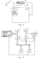
- Fig. 1 shows a block diagram of a bus system of a first embodiment of the present invention.
- the bus system in this embodiment is a multilayer system.
- the multilayer system basically includes a plurality of masters 1 (M0, M1, M2), a plurality of slaves 3 (S0, S1, S2), and a multilayer switch 2 disposed between the masters 1 and the slaves 3.
- the multilayer system further includes an access control register 4.
- the master 1 is a module that controls the system, such as Central Processor Unit (CPU), Digital Signal Processor (DSP), image rotating device, camera image processing circuit, Liquid Crystal Display (LCD) controller, and so on.
- the M0 is a processing circuit such as CPU and DSP that always operate.
- the M1 and M2 are modules that operate as needed according to instructions from the M0.
- the multilayer switch 2 allows simultaneous processing of commands from a plurality of masters.
- the multilayer switch 2 is an interconnection bus system that allows use of a parallel access path between a plurality of masters and slaves in the system.
- the bus system is realized by use of a more complex interconnection matrix and provides advantages such as increase in architecture options and in the entire bus bandwidth.
- the multilayer switch 2 is offered by ARM Ltd. as Advanced High-performance Bus (AHB), AHB-Lite®, for example.
- the slave 3 is a module that is controlled by the master 1.
- the slave 3 includes a memory, a register, a timer, a serial interface circuit, and so on.
- the configuration of the multilayer switch 2 is described in detail below.
- the multilayer switch 2 has switch master portions 20 (SWMO, SWM1, SWM2) connected to each of the masters 1 (M0, M1, M2), and switch slave portions 21 (SWS0, SWS1, SWS2) connected to each of the slaves 3.
- the switch master portion 20 has the function that determines which slave 3 is to be connected in response to the access from the master 1 based on address information specifying an access destination and sends an access request to the switch slave portion 21 corresponding to the slave 3 to be connected. Further, the switch master portion 20 in this embodiment has an address comparator circuit, though not shown. The address comparator circuit compares address information included in the access control information from the access control register 4 with address information included in the access from the master 1, and, if they match, controls the access to the slave specified by the address information.
- the key function of the switch slave portion 21 is to arbitrate the access signals from each switch master portion 20, select one access and make a connection to the selected slave 3.
- the access control register 4 includes a range setting register 40 and a control target register 41 to store access control information.
- the access control information includes control range information and control target information.
- the control range information specifies an access control area in the slave 3, and is stored in the range setting register 40.
- the control target information specifies for which master 1 the access control should be activated, and is stored in the control target register 41.
- Information can be set to the range setting register 40 and the control target register 41 only by the M0, which is a secure master.
- Other masters such as the M1 and M2 cannot set the information. It is preferred to create a hardware configuration so as to allow the only M0, the secure master, to set information to the range setting register 40 and the control target register 41.
- the secure master M0 is connected to a local bus, and the area where the master different from the M0 cannot access the address comparator circuit is created by default.
- the range setting register 40 and the control target register 41 are connected to the SWM1 and SWM2 by signal lines.
- the address comparator circuits included in the SWM1 and SWM2 are connected to the range setting register 40 and the control target register 41 by signal lines.
- detecting the voltage of these signal lines allows recognizing the address control information stored in the range setting register 40 and the control target register 41.
- S2 is a memory that stores confidential information in the addresses 8000 to FFFF. Access is controlled to these addresses from the masters 1 other than the M0, which are M1 and M2 for example.
- M1 and M2 for example.
- the M1 outputs an address signal ("8000") of an access destination (the S2 in this case) and a control signal such as a read/write signal to the SWM1, which is the switch master portion 20 of the multilayer switch 2.
- the SWM1 determines which slave 3 is to be accessed based on the address signal from the M1. Further, in the SWM1, the address comparator circuit compares address information included in the address signal from the M1 with address information included in the control range information set to the range setting register 40. Since the area of the addresses 8000 to FFFF is set to the range setting register 40 as an access control area in this case, the SWM1 operates with a recognition that the address 8000 where the M1 tries to access is within the control range. Thus, the SWM1 determines that the M1 makes an access to the access control area. In this case, the SWM1 does not transmit transaction to the SWS2 of the multilayer switch 2, but sends an error response to the M1 to inhibit the access to the access control area.
- the switch master portion 20 performs access control with reference to the access control register 4 in this embodiment. Thus, even if a specific master repeatedly accesses the slave under access control, the access to the switch slave portion 21 and the slave 3 does not occur, thereby preventing decrease in the bus access performance of the master different from the specific master connected to the multilayer switch 2.
- the access control area may be set to a given area of the system memory map. This embodiment also allows setting which master is inhibited to access the set area.
- Fig. 2 shows a layout example of a chip 100 and a circuit configuration example of elements related to power supply. As shown in Fig. 2 , power is constantly supplied to the M0 and the access control register 4 from a power supply 51. On the other hand, power is supplied to the other circuits including the M1 via a power supply control circuit 52. The power supply control circuit 52 operates in accordance with the control by the M0, and it stops power supply to each master 1, slave 3, and so on when not needed. This achieves power saving in the chip 100.
- a second embodiment of the present invention uses a normal bus, not a multilayer system.
- Fig. 3 shows the configuration of a bus system according to the second embodiment.
- a switch 6 is placed between the connection point of a system bus 8 and a master 1.
- the address of an access destination of M1 is input to an arbiter 7.
- Access control information stored in the range setting register 40 and the control target register 41 is also input to the arbiter 7.
- the access control information can be set to the access control register 4 only by the M0, which is a secure master.
- the arbiter 7 has a function to set authorization to use the system bus 8 by the master 1.
- the M1 outputs the address signal of an access destination to the arbiter 7.
- the arbiter 7 compares address information included in this address signal with address information included in access control information stored in the access control register 4, and outputs a comparison result.
- the arbiter 7 determines that the M1 makes an access to the set access control area.
- the arbiter 7 requests the switch 6 between the M1 and the connection point of the system bus 8 to prevent the access from the M1 to the system bus 8.
- the switch 6 sends an error response signal indicating that the access is inhibited to the master. This prevents the M1 from accessing the access control area.
- the arbiter 7 performs access control with reference to the access control register 4 using the switch 6 placed between the connection point of the system bus 8 and the master 1 in this embodiment. Thus, even if a specific master repeatedly accesses the slave under the access control, the access to the system bus 8 does not occur, thereby preventing decrease in the system bus performance.
- the access control area may be set to a given area of the system memory map. This embodiment also allows setting which master is inhibited to access the set area.
- the bus system includes a plurality of masters, a plurality of slaves, and a multilayer switch.
- the bus system further includes an access control register to which access control information is set by a predetermined secure master.
- the multilayer switch includes switch master portions and switch slave portions. When a master accesses a slave, a switch master portion corresponding to a master different from the secure master determines whether the access is made to an access control area based on address information of an access destination and access control information stored in the access control register. If the switch master portion determines that the access is made to the access control area, it inhibits the access.
Landscapes
- Engineering & Computer Science (AREA)
- Physics & Mathematics (AREA)
- General Engineering & Computer Science (AREA)
- Theoretical Computer Science (AREA)
- Mathematical Physics (AREA)
- Computer Hardware Design (AREA)
- General Physics & Mathematics (AREA)
- Small-Scale Networks (AREA)
- Bus Control (AREA)
- Storage Device Security (AREA)
Claims (16)
- Bussystem, das Folgendes aufweist:eine Vielzahl von Hauptrechnern (1);eine Vielzahl von Nebenrechnern (3);einen zwischen den Hauptrechnern und den Nebenrechnern angeordneten mehrschichtigen Schalter (2), der Befehle von der Vielzahl von Hauptrechnern gleichzeitig verarbeitet und der Schalter-Hauptrechnerabschnitte (20) entsprechend den Hauptrechnern und Schalter-Nebenrechnerabschnitte (21) entsprechend den Nebenrechnern aufweist; undein Zugriffsbefehlsregister (4), zu dem durch einen vorbestimmten sicheren Hauptrechner Zugriffssteuerinformation eingestellt wird;wobei auf ein Auftreten eines Zugriffs von einem Hauptrechner auf einen Nebenrechner hin ein Schalter-Hauptrechnerabschnitt entsprechend einem vom sicheren Hauptrechner unterschiedlichen Hauptrechner basierend auf Adresseninformation eines Zugriffszielorts und im Zugriffssteuerregister gespeicherter Zugriffssteuerinformation bestimmt, ob der Zugriff auf einen Zugriffssteuerbereich durchgeführt wird, und dann, wenn er bestimmt, dass der Zugriff auf den Zugriffssteuerbereich durchgeführt wird, den Zugriff verhindert.
- Bussystem nach Anspruch 1, wobei dem sicheren Hauptrechner und dem Zugriffssteuerregister konstant Strom zugeführt wird.
- Bussystem nach Anspruch 2, wobei eine Stromversorgung zu dem vom sicheren Hauptrechner unterschiedlichen Hauptrechner und/oder dem Nebenrechner durch den sicheren Hauptrechner gesteuert wird.
- Bussystem nach einem der Ansprüche 1 bis 3, wobei das Zugriffssteuerregister ein Reichweiteeinstellregister (40), das Reichweiteeinstellinformation speichert, die einen Zugriffssteuerbereich einstellt, und ein Steuerzielregister (41), das Steuerzielinformation speichert, die einen zu steuernden Hauptrechner spezifiziert, aufweist.
- Bussystem, das Folgendes aufweist:eine Vielzahl von Hauptrechnern (1);eine Vielzahl von Nebenrechnern (3);einen Systembus (8), mit dem die Hauptrechner und die Nebenrechner verbunden sind;einen Zuteiler (7), der eine Berechtigung zum Verwenden des Systembusses einstellt;ein Zugriffssteuerregister (4), zu dem Zugriffssteuerinformation durch einen vorbestimmten sicheren Hauptrechner eingestellt wird; undeinen Schalter (6), der zwischen einem vom sicheren Hauptrechner unterschiedlichen Hauptrechner und dem Systembus angeordnet ist,wobei auf ein Auftreten eines Zugriffs von einem vom sicheren Hauptrechner unterschiedlichen Hauptrechner auf den Nebenrechner hin der Zuteiler basierend auf Adresseninformation eines Zugriffszielorts und auf im Zugriffssteuerregister gespeicherter Zugriffssteuerinformation bestimmt, ob der Zugriff auf einen Zugriffssteuerbereich durchgeführt wird, und dann, wenn er bestimmt, dass der Zugriff auf den Zugriffssteuerbereich durchgeführt wird, der Schalter den Hauptrechner, der den Zugriff durchführt, von einem Zugreifen auf den Systembus abhält.
- Bussystem nach Anspruch 5, wobei dem sicheren Hauptrechner und dem Zugriffssteuerregister konstant Strom zugeführt wird.
- Bussystem nach Anspruch 6, wobei eine Stromversorgung zu dem vom sicheren Hauptrechner unterschiedlichen Hauptrechner und/oder dem Nebenrechner durch den sicheren Hauptrechner gesteuert wird.
- Bussystem nach einem der Ansprüche 5 bis 7, wobei das Zugriffssteuerregister ein Reichweiteeinstellregister (40), das Reichweiteeinstellinformation speichert, die einen Zugriffssteuerbereich einstellt, und ein Steuerzielregister (41), das Steuerzielinformation speichert, die einen zu steuernden Hauptrechner spezifiziert, aufweist.
- Zugriffssteuerverfahren in einem Bussystem mit einer Vielzahl von Hauptrechnern (1), einer Vielzahl von Nebenrechnern (3) und einem mehrschichtigen Schalter (2), der zwischen den Hauptrechnern und den Nebenrechnern angeordnet ist und Befehle von der Vielzahl von Hauptrechnern gleichzeitig verarbeitet, wobei der mehrschichtige Schalter Schalter-Hauptrechnerabschnitte (20) entsprechend den Hauptrechnern und Schalter-Nebenrechnerabschnitte (21) entsprechend den Nebenrechnern hat, wobei das Verfahren Folgendes aufweist:Einstellen von Zugriffssteuerinformation zu einem Zugriffssteuerregister (4) durch einen vorbestimmten sicheren Hauptrechner;auf ein Auftreten eines Zugriffs von einem vom sicheren Hauptrechner unterschiedlichen Hauptrechner auf einen Nebenrechner hin, Vergleichen von Adresseninformation eines Zugriffszielorts mit zum Zugriffsteuerregister eingestellter Zugriffssteuerinformation und Bestimmen, ob der Zugriff auf einen Zugriffssteuerbereich durchgeführt wird; undauf eine Bestimmung hin, dass der Zugriff auf den Zugriffssteuerbereich durchgeführt wird, Verhindern des Zugriffs durch den Schalter-Hauptrechnerabschnitt entsprechend dem Hauptrechner, der den Zugriff durchführt.
- Zugriffssteuerverfahren nach Anspruch 9, wobei dem sicheren Hauptrechner und dem Zugriffsbefehlsregister konstant Strom zugeführt wird.
- Zugriffssteuerverfahren nach Anspruch 10, wobei eine Stromversorgung zu dem vom sicheren Hauptrechner unterschiedlichen Hauptrechner und/oder dem Nebenrechner durch den sicheren Hauptrechner gesteuert wird.
- Zugriffssteuerverfahren nach einem der Ansprüche 9 bis 11, wobei das Zugriffssteuerregister ein Reichweiteeinstellregister (40), das Reichweiteeinstellinformation speichert, die einen Zugriffssteuerbereich einstellt, und ein Steuerzielregister (41), das Steuerzielinformation speichert, die einen zu steuernden Hauptrechner spezifiziert, aufweist.
- Zugriffssteuerverfahren in einem Bussystem mit einer Vielzahl von Hauptrechnern (1), einer Vielzahl von Nebenrechnern (3), einem Systembus (8), mit dem die Hauptrechner und die Nebenrechner verbunden sind, und einem Zuteiler (7), der eine Berechtigung zum Verwenden des Bussystems einstellt, wobei das Verfahren Folgendes aufweist:Einstellen von Zugriffssteuerinformation zu einem Zugriffssteuerregister durch einen vorbestimmten sicheren Hauptrechner;auf ein Auftreten eines Zugriffs von einem vom sicheren Hauptrechner unterschiedlichen Hauptrechner auf einen Nebenrechner hin, Bestimmen, ob der Zugriff auf einen Zugriffssteuerbereich durchgeführt wird, durch den Zuteiler basierend auf Adresseninformation eines Zugriffszielorts und auf zum Zugriffssteuerregister eingestellter Zugriffssteuerinformation, undauf eine Bestimmung, dass der Zugriff auf den Zugriffssteuerbereich durchgeführt wird, durch den Zuteiler hin Abhalten des Hautrechners, der den Zugriff durchführt, von einem Zugreifen auf den Systembus durch einen zwischen den Hauptrechnern und dem Systembus angeordneten Schalter (6).
- Zugriffssteuerverfahren nach Anspruch 13, wobei dem sicheren Hauptrechner und dem Zugriffsbefehlsregister konstant Strom zugeführt wird.
- Zugriffssteuerverfahren nach Anspruch 14, wobei eine Stromversorgung zu dem vom sicheren Hauptrechner unterschiedlichen Hauptrechner und/oder dem Nebenrechner durch den sicheren Hauptrechner gesteuert wird.
- Zugriffssteuerverfahren nach einem der Ansprüche 13 bis 15, wobei das Zugriffssteuerregister ein Reichweiteeinstellregister (40), das Reichweiteeinstellinformation speichert, die einen Zugriffssteuerbereich einstellt, und ein Steuerzielregister (41), das Steuerzielinformation speichert, die einen zu steuernden Hauptrechner spezifiziert, aufweist.
Applications Claiming Priority (2)
| Application Number | Priority Date | Filing Date | Title |
|---|---|---|---|
| JP2004060172 | 2004-03-04 | ||
| JP2004060172A JP2005250833A (ja) | 2004-03-04 | 2004-03-04 | バスシステム及びアクセス制御方法 |
Publications (2)
| Publication Number | Publication Date |
|---|---|
| EP1571559A1 EP1571559A1 (de) | 2005-09-07 |
| EP1571559B1 true EP1571559B1 (de) | 2008-05-21 |
Family
ID=34747656
Family Applications (1)
| Application Number | Title | Priority Date | Filing Date |
|---|---|---|---|
| EP05101644A Expired - Lifetime EP1571559B1 (de) | 2004-03-04 | 2005-03-03 | Bussystem und Zugangsteuerungsverfahren |
Country Status (5)
| Country | Link |
|---|---|
| US (1) | US20050235084A1 (de) |
| EP (1) | EP1571559B1 (de) |
| JP (1) | JP2005250833A (de) |
| CN (1) | CN100356354C (de) |
| DE (1) | DE602005006867D1 (de) |
Families Citing this family (37)
| Publication number | Priority date | Publication date | Assignee | Title |
|---|---|---|---|---|
| JP4477380B2 (ja) * | 2004-03-02 | 2010-06-09 | Necエレクトロニクス株式会社 | マルチレイヤシステム及びクロック制御方法 |
| JP2006195746A (ja) * | 2005-01-13 | 2006-07-27 | Oki Electric Ind Co Ltd | マルチレイヤバスシステム |
| JP2007219678A (ja) * | 2006-02-15 | 2007-08-30 | Oki Electric Ind Co Ltd | マルチレイヤバス・システム |
| EP1830268B1 (de) * | 2006-03-03 | 2019-05-08 | STMicroelectronics (Research & Development) Limited | Integrierte Mehrzweckschaltung |
| US8156273B2 (en) * | 2007-05-10 | 2012-04-10 | Freescale Semiconductor, Inc. | Method and system for controlling transmission and execution of commands in an integrated circuit device |
| CN101334760B (zh) * | 2007-06-26 | 2010-04-07 | 展讯通信(上海)有限公司 | 监控总线非法操作的方法、装置及包含该装置的系统 |
| US8433838B2 (en) * | 2010-09-17 | 2013-04-30 | International Business Machines Corporation | Remote multiplexing devices on a serial peripheral interface bus |
| US8595366B2 (en) * | 2011-05-05 | 2013-11-26 | Qualcomm Incorporated | Method and system for dynamically creating and servicing master-slave pairs within and across switch fabrics of a portable computing device |
| KR101819235B1 (ko) * | 2011-06-08 | 2018-01-16 | 엘에스산전 주식회사 | 병렬 통신 장치 |
| EP2568407B1 (de) * | 2011-09-09 | 2017-10-25 | Assa Abloy Ab | Verfahren und System zur Kommunikation mit einem sicheren Element und zu seiner Steuerung |
| US9191203B2 (en) | 2013-08-06 | 2015-11-17 | Bedrock Automation Platforms Inc. | Secure industrial control system |
| US8868813B2 (en) | 2011-12-30 | 2014-10-21 | Bedrock Automation Platforms Inc. | Communications control system with a serial communications interface and a parallel communications interface |
| US11967839B2 (en) | 2011-12-30 | 2024-04-23 | Analog Devices, Inc. | Electromagnetic connector for an industrial control system |
| EP3249758B1 (de) * | 2011-12-30 | 2020-05-13 | Bedrock Automation Platforms Inc. | Elektromagnetischer verbinder und kommunikations-/steuerungssystem/koppelfeld mit seriellen und parallelen kommunikationsschnittstellen |
| US8862802B2 (en) | 2011-12-30 | 2014-10-14 | Bedrock Automation Platforms Inc. | Switch fabric having a serial communications interface and a parallel communications interface |
| US9600434B1 (en) | 2011-12-30 | 2017-03-21 | Bedrock Automation Platforms, Inc. | Switch fabric having a serial communications interface and a parallel communications interface |
| US10834094B2 (en) | 2013-08-06 | 2020-11-10 | Bedrock Automation Platforms Inc. | Operator action authentication in an industrial control system |
| US9727511B2 (en) | 2011-12-30 | 2017-08-08 | Bedrock Automation Platforms Inc. | Input/output module with multi-channel switching capability |
| US12061685B2 (en) | 2011-12-30 | 2024-08-13 | Analog Devices, Inc. | Image capture devices for a secure industrial control system |
| US9467297B2 (en) | 2013-08-06 | 2016-10-11 | Bedrock Automation Platforms Inc. | Industrial control system redundant communications/control modules authentication |
| US10834820B2 (en) | 2013-08-06 | 2020-11-10 | Bedrock Automation Platforms Inc. | Industrial control system cable |
| US9437967B2 (en) | 2011-12-30 | 2016-09-06 | Bedrock Automation Platforms, Inc. | Electromagnetic connector for an industrial control system |
| US8971072B2 (en) | 2011-12-30 | 2015-03-03 | Bedrock Automation Platforms Inc. | Electromagnetic connector for an industrial control system |
| US11314854B2 (en) | 2011-12-30 | 2022-04-26 | Bedrock Automation Platforms Inc. | Image capture devices for a secure industrial control system |
| US11144630B2 (en) | 2011-12-30 | 2021-10-12 | Bedrock Automation Platforms Inc. | Image capture devices for a secure industrial control system |
| US10613567B2 (en) | 2013-08-06 | 2020-04-07 | Bedrock Automation Platforms Inc. | Secure power supply for an industrial control system |
| US9619410B1 (en) * | 2013-10-03 | 2017-04-11 | Jpmorgan Chase Bank, N.A. | Systems and methods for packet switching |
| JP6246036B2 (ja) * | 2014-03-19 | 2017-12-13 | 三菱電機株式会社 | 中継装置 |
| US9268970B2 (en) | 2014-03-20 | 2016-02-23 | Analog Devices, Inc. | System and method for security-aware master |
| CN111293495B (zh) | 2014-07-07 | 2022-05-24 | 基岩自动化平台公司 | 工业控制系统电缆 |
| EP3298500B1 (de) * | 2015-05-22 | 2021-08-25 | Hewlett-Packard Development Company, L.P. | Datenkanalzuweisung |
| US11416421B2 (en) * | 2016-07-19 | 2022-08-16 | Cypress Semiconductor Corporation | Context-based protection system |
| JP7199885B2 (ja) * | 2018-09-14 | 2023-01-06 | キヤノン株式会社 | メモリ制御装置 |
| CN111382100A (zh) * | 2018-12-29 | 2020-07-07 | 深圳市优必选科技有限公司 | 一种i2c总线的数据采集方法及系统 |
| EP4092556B1 (de) | 2021-05-20 | 2026-08-19 | Nordic Semiconductor ASA | Busdecoder |
| KR20240159791A (ko) * | 2023-04-28 | 2024-11-06 | 쑤저우 메타브레인 인텔리전트 테크놀로지 컴퍼니 리미티드 | 운영체제 실행 제어 방법과 장치, 및 임베디드 시스템과 칩 |
| CN119668960B (zh) * | 2024-12-04 | 2025-09-19 | 北京芯驰半导体科技股份有限公司 | 一种ahb传输的错误检测方法和ahb信号处理器 |
Family Cites Families (11)
| Publication number | Priority date | Publication date | Assignee | Title |
|---|---|---|---|---|
| US4797853A (en) * | 1985-11-15 | 1989-01-10 | Unisys Corporation | Direct memory access controller for improved system security, memory to memory transfers, and interrupt processing |
| US4979853A (en) * | 1990-01-26 | 1990-12-25 | Ford Motor Company | Cutting tool holder for high speed spindle machining system |
| US5168564A (en) * | 1990-10-05 | 1992-12-01 | Bull Hn Information Systems Inc. | Cancel mechanism for resilient resource management and control |
| JP2904991B2 (ja) * | 1992-03-13 | 1999-06-14 | オークマ株式会社 | 数値制御装置 |
| JPH10506489A (ja) * | 1994-11-17 | 1998-06-23 | シーメンス アクチエンゲゼルシヤフト | マスターおよびスレイブ−ユニットを有する装置 |
| US6691193B1 (en) * | 2000-10-18 | 2004-02-10 | Sony Corporation | Efficient bus utilization in a multiprocessor system by dynamically mapping memory addresses |
| US7076595B1 (en) * | 2001-05-18 | 2006-07-11 | Xilinx, Inc. | Programmable logic device including programmable interface core and central processing unit |
| US7277972B2 (en) * | 2002-03-08 | 2007-10-02 | Freescale Semiconductor, Inc. | Data processing system with peripheral access protection and method therefor |
| US6851056B2 (en) * | 2002-04-18 | 2005-02-01 | International Business Machines Corporation | Control function employing a requesting master id and a data address to qualify data access within an integrated system |
| DE10222584A1 (de) * | 2002-05-22 | 2003-12-11 | Infineon Technologies Ag | Verfahren und System zur Vergabe und Verwaltung von Zugriffsrechten für die Master in Multimaster Bussystemen |
| US20030221030A1 (en) * | 2002-05-24 | 2003-11-27 | Timothy A. Pontius | Access control bus system |
-
2004
- 2004-03-04 JP JP2004060172A patent/JP2005250833A/ja active Pending
-
2005
- 2005-03-01 CN CNB2005100525443A patent/CN100356354C/zh not_active Expired - Fee Related
- 2005-03-03 US US11/069,947 patent/US20050235084A1/en not_active Abandoned
- 2005-03-03 DE DE602005006867T patent/DE602005006867D1/de not_active Expired - Lifetime
- 2005-03-03 EP EP05101644A patent/EP1571559B1/de not_active Expired - Lifetime
Also Published As
| Publication number | Publication date |
|---|---|
| EP1571559A1 (de) | 2005-09-07 |
| CN100356354C (zh) | 2007-12-19 |
| DE602005006867D1 (de) | 2008-07-03 |
| US20050235084A1 (en) | 2005-10-20 |
| CN1664799A (zh) | 2005-09-07 |
| JP2005250833A (ja) | 2005-09-15 |
Similar Documents
| Publication | Publication Date | Title |
|---|---|---|
| EP1571559A1 (de) | Bussystem und Zugangsteuerungsverfahren | |
| US20040177266A1 (en) | Data processing system with peripheral access protection and method therefor | |
| US6145029A (en) | Computer system with enhanced docking support | |
| US5727171A (en) | Method and apparatus for allowing multi-speed synchronous communications between a processor and both slow and fast computing devices | |
| US7277972B2 (en) | Data processing system with peripheral access protection and method therefor | |
| US6272580B1 (en) | Apparatus and method for dynamically elevating a lower level bus master to an upper level bus master within a multi-level arbitration system | |
| EP1938190B1 (de) | Verfahren und vorrichtung zur löschung von semaphorreservierungen | |
| JP4945053B2 (ja) | 半導体装置、バスインターフェース装置、およびコンピュータシステム | |
| EP1685484B1 (de) | Speicherschnittstelle für systeme mit mehreren prozessoren und einem speichersystem | |
| US20040221173A1 (en) | Method and apparatus for endianness control in a data processing system | |
| US6247087B1 (en) | Bus system for shadowing registers | |
| US5933613A (en) | Computer system and inter-bus control circuit | |
| TWI245222B (en) | Accessing configuration registers by automatically changing an index | |
| US6757798B2 (en) | Method and apparatus for arbitrating deferred read requests | |
| US6460139B1 (en) | Apparatus and method for programmably and flexibly assigning passwords to unlock devices of a computer system intended to remain secure | |
| US7080176B2 (en) | Bus control device and information processing system | |
| US7343436B2 (en) | Synchronous electronic control system and system control method | |
| US20050198429A1 (en) | Multilayer system and clock control method | |
| JPH09153009A (ja) | 階層構成バスのアービトレーション方法 | |
| US5875338A (en) | Method and apparatus for arbitrating resource requests utilizing independent tokens for arbiter cell selection | |
| JPH10301657A (ja) | コンピュータシステムの周辺デバイス | |
| EP1984943B1 (de) | Selektive transaktionsanforderungsverarbeitung in einer verbindungsanordnung während eines lockout | |
| KR100210404B1 (ko) | 공유 메모리 억세스 제어장치 | |
| JP2671743B2 (ja) | マイクロコンピュータ | |
| JPH0991152A (ja) | コンピュータシステムおよびそのシステムで使用されるマルチファンクションデバイス |
Legal Events
| Date | Code | Title | Description |
|---|---|---|---|
| PUAI | Public reference made under article 153(3) epc to a published international application that has entered the european phase |
Free format text: ORIGINAL CODE: 0009012 |
|
| AK | Designated contracting states |
Kind code of ref document: A1 Designated state(s): AT BE BG CH CY CZ DE DK EE ES FI FR GB GR HU IE IS IT LI LT LU MC NL PL PT RO SE SI SK TR |
|
| AX | Request for extension of the european patent |
Extension state: AL BA HR LV MK YU |
|
| 17P | Request for examination filed |
Effective date: 20051202 |
|
| AKX | Designation fees paid |
Designated state(s): DE GB |
|
| 17Q | First examination report despatched |
Effective date: 20061222 |
|
| GRAP | Despatch of communication of intention to grant a patent |
Free format text: ORIGINAL CODE: EPIDOSNIGR1 |
|
| GRAS | Grant fee paid |
Free format text: ORIGINAL CODE: EPIDOSNIGR3 |
|
| GRAA | (expected) grant |
Free format text: ORIGINAL CODE: 0009210 |
|
| AK | Designated contracting states |
Kind code of ref document: B1 Designated state(s): DE GB |
|
| REG | Reference to a national code |
Ref country code: GB Ref legal event code: FG4D |
|
| REF | Corresponds to: |
Ref document number: 602005006867 Country of ref document: DE Date of ref document: 20080703 Kind code of ref document: P |
|
| PLBE | No opposition filed within time limit |
Free format text: ORIGINAL CODE: 0009261 |
|
| STAA | Information on the status of an ep patent application or granted ep patent |
Free format text: STATUS: NO OPPOSITION FILED WITHIN TIME LIMIT |
|
| 26N | No opposition filed |
Effective date: 20090224 |
|
| REG | Reference to a national code |
Ref country code: DE Ref legal event code: R082 Ref document number: 602005006867 Country of ref document: DE Representative=s name: BETTEN & RESCH, DE |
|
| REG | Reference to a national code |
Ref country code: DE Ref legal event code: R081 Ref document number: 602005006867 Country of ref document: DE Owner name: RENESAS ELECTRONICS CORPORATION, JP Free format text: FORMER OWNER: NEC ELECTRONICS CORP., KAWASAKI, JP Effective date: 20120828 Ref country code: DE Ref legal event code: R082 Ref document number: 602005006867 Country of ref document: DE Representative=s name: PATENTANWAELTE BETTEN & RESCH, DE Effective date: 20120828 Ref country code: DE Ref legal event code: R081 Ref document number: 602005006867 Country of ref document: DE Owner name: RENESAS ELECTRONICS CORPORATION, KAWASAKI-SHI, JP Free format text: FORMER OWNER: NEC ELECTRONICS CORP., KAWASAKI, KANAGAWA, JP Effective date: 20120828 Ref country code: DE Ref legal event code: R082 Ref document number: 602005006867 Country of ref document: DE Representative=s name: BETTEN & RESCH PATENT- UND RECHTSANWAELTE PART, DE Effective date: 20120828 |
|
| PGFP | Annual fee paid to national office [announced via postgrant information from national office to epo] |
Ref country code: DE Payment date: 20130227 Year of fee payment: 9 Ref country code: GB Payment date: 20130228 Year of fee payment: 9 |
|
| REG | Reference to a national code |
Ref country code: DE Ref legal event code: R119 Ref document number: 602005006867 Country of ref document: DE |
|
| GBPC | Gb: european patent ceased through non-payment of renewal fee |
Effective date: 20140303 |
|
| REG | Reference to a national code |
Ref country code: DE Ref legal event code: R119 Ref document number: 602005006867 Country of ref document: DE Effective date: 20141001 |
|
| PG25 | Lapsed in a contracting state [announced via postgrant information from national office to epo] |
Ref country code: DE Free format text: LAPSE BECAUSE OF NON-PAYMENT OF DUE FEES Effective date: 20141001 Ref country code: GB Free format text: LAPSE BECAUSE OF NON-PAYMENT OF DUE FEES Effective date: 20140303 |