EP1569283B1 - LED mit optischem System zum Erhöhen der Luminanz durch Recycling des ausgestrahlten Lichts - Google Patents
LED mit optischem System zum Erhöhen der Luminanz durch Recycling des ausgestrahlten Lichts Download PDFInfo
- Publication number
- EP1569283B1 EP1569283B1 EP05100195A EP05100195A EP1569283B1 EP 1569283 B1 EP1569283 B1 EP 1569283B1 EP 05100195 A EP05100195 A EP 05100195A EP 05100195 A EP05100195 A EP 05100195A EP 1569283 B1 EP1569283 B1 EP 1569283B1
- Authority
- EP
- European Patent Office
- Prior art keywords
- wedge
- transparent member
- light emitting
- light
- emitting diode
- Prior art date
- Legal status (The legal status is an assumption and is not a legal conclusion. Google has not performed a legal analysis and makes no representation as to the accuracy of the status listed.)
- Expired - Lifetime
Links
- 230000003287 optical effect Effects 0.000 title claims description 46
- 238000004064 recycling Methods 0.000 title 1
- 238000000576 coating method Methods 0.000 claims description 18
- 239000011248 coating agent Substances 0.000 claims description 16
- 239000000463 material Substances 0.000 claims description 16
- 239000011521 glass Substances 0.000 claims description 4
- 239000010980 sapphire Substances 0.000 claims description 3
- 229910052594 sapphire Inorganic materials 0.000 claims description 3
- NIXOWILDQLNWCW-UHFFFAOYSA-N acrylic acid group Chemical group C(C=C)(=O)O NIXOWILDQLNWCW-UHFFFAOYSA-N 0.000 claims description 2
- 229920001296 polysiloxane Polymers 0.000 claims description 2
- 239000007787 solid Substances 0.000 description 7
- 230000005855 radiation Effects 0.000 description 6
- 238000009826 distribution Methods 0.000 description 4
- 238000005286 illumination Methods 0.000 description 4
- 229910052751 metal Inorganic materials 0.000 description 4
- 239000002184 metal Substances 0.000 description 4
- PCHJSUWPFVWCPO-UHFFFAOYSA-N gold Chemical compound [Au] PCHJSUWPFVWCPO-UHFFFAOYSA-N 0.000 description 3
- 229910052737 gold Inorganic materials 0.000 description 3
- 239000010931 gold Substances 0.000 description 3
- 229920003023 plastic Polymers 0.000 description 3
- 239000004065 semiconductor Substances 0.000 description 3
- 239000000758 substrate Substances 0.000 description 3
- OAICVXFJPJFONN-UHFFFAOYSA-N Phosphorus Chemical compound [P] OAICVXFJPJFONN-UHFFFAOYSA-N 0.000 description 2
- 238000004026 adhesive bonding Methods 0.000 description 2
- JNDMLEXHDPKVFC-UHFFFAOYSA-N aluminum;oxygen(2-);yttrium(3+) Chemical compound [O-2].[O-2].[O-2].[Al+3].[Y+3] JNDMLEXHDPKVFC-UHFFFAOYSA-N 0.000 description 2
- TZCXTZWJZNENPQ-UHFFFAOYSA-L barium sulfate Chemical compound [Ba+2].[O-]S([O-])(=O)=O TZCXTZWJZNENPQ-UHFFFAOYSA-L 0.000 description 2
- 239000002800 charge carrier Substances 0.000 description 2
- 239000000835 fiber Substances 0.000 description 2
- 230000004907 flux Effects 0.000 description 2
- 238000003384 imaging method Methods 0.000 description 2
- 239000004033 plastic Substances 0.000 description 2
- 238000003825 pressing Methods 0.000 description 2
- 229910019901 yttrium aluminum garnet Inorganic materials 0.000 description 2
- 239000004593 Epoxy Substances 0.000 description 1
- VYPSYNLAJGMNEJ-UHFFFAOYSA-N Silicium dioxide Chemical compound O=[Si]=O VYPSYNLAJGMNEJ-UHFFFAOYSA-N 0.000 description 1
- BQCADISMDOOEFD-UHFFFAOYSA-N Silver Chemical compound [Ag] BQCADISMDOOEFD-UHFFFAOYSA-N 0.000 description 1
- 238000010521 absorption reaction Methods 0.000 description 1
- 229910052782 aluminium Inorganic materials 0.000 description 1
- XAGFODPZIPBFFR-UHFFFAOYSA-N aluminium Chemical compound [Al] XAGFODPZIPBFFR-UHFFFAOYSA-N 0.000 description 1
- 150000001875 compounds Chemical class 0.000 description 1
- 230000003247 decreasing effect Effects 0.000 description 1
- 230000000694 effects Effects 0.000 description 1
- 238000001652 electrophoretic deposition Methods 0.000 description 1
- 238000000605 extraction Methods 0.000 description 1
- 239000005350 fused silica glass Substances 0.000 description 1
- 239000003292 glue Substances 0.000 description 1
- 238000010438 heat treatment Methods 0.000 description 1
- 150000002739 metals Chemical class 0.000 description 1
- 238000000034 method Methods 0.000 description 1
- 239000000203 mixture Substances 0.000 description 1
- 239000013307 optical fiber Substances 0.000 description 1
- 238000012634 optical imaging Methods 0.000 description 1
- 239000003973 paint Substances 0.000 description 1
- 238000010422 painting Methods 0.000 description 1
- 239000000843 powder Substances 0.000 description 1
- 238000002310 reflectometry Methods 0.000 description 1
- 229910052703 rhodium Inorganic materials 0.000 description 1
- 239000010948 rhodium Substances 0.000 description 1
- MHOVAHRLVXNVSD-UHFFFAOYSA-N rhodium atom Chemical compound [Rh] MHOVAHRLVXNVSD-UHFFFAOYSA-N 0.000 description 1
- 238000000926 separation method Methods 0.000 description 1
- 229910052709 silver Inorganic materials 0.000 description 1
- 239000004332 silver Substances 0.000 description 1
- 229910000679 solder Inorganic materials 0.000 description 1
- 239000000126 substance Substances 0.000 description 1
Images


Classifications
-
- H—ELECTRICITY
- H10—SEMICONDUCTOR DEVICES; ELECTRIC SOLID-STATE DEVICES NOT OTHERWISE PROVIDED FOR
- H10H—INORGANIC LIGHT-EMITTING SEMICONDUCTOR DEVICES HAVING POTENTIAL BARRIERS
- H10H20/00—Individual inorganic light-emitting semiconductor devices having potential barriers, e.g. light-emitting diodes [LED]
- H10H20/80—Constructional details
- H10H20/85—Packages
- H10H20/855—Optical field-shaping means, e.g. lenses
-
- H—ELECTRICITY
- H10—SEMICONDUCTOR DEVICES; ELECTRIC SOLID-STATE DEVICES NOT OTHERWISE PROVIDED FOR
- H10H—INORGANIC LIGHT-EMITTING SEMICONDUCTOR DEVICES HAVING POTENTIAL BARRIERS
- H10H20/00—Individual inorganic light-emitting semiconductor devices having potential barriers, e.g. light-emitting diodes [LED]
- H10H20/80—Constructional details
- H10H20/85—Packages
- H10H20/851—Wavelength conversion means
- H10H20/8515—Wavelength conversion means not being in contact with the bodies
Definitions
- the present invention relates generally to increasing the brightness of a light emitting diode light source.
- Fig. 1 illustrates a lens 12 transmitting light generated by a light source 10 such as a light emitting diode.
- a light source 10 such as a light emitting diode.
- Etendue is a geometric property of the optics related to the divergence and cross-sectional area of the beam. The etendue cannot be decreased for if it were, the energy density at the image could exceed that of the source, violating the second law of thermodynamics.
- Source 10 may be, for example, a light emitting diode (LED), which emits light in all directions. As illustrated in Fig. 1 , only light 16 emitted from the center of the top surface of source 10 and within the cone accepted by the lens can be focused on the target 20. Light 14 emitted from the top of source 10 far from lens 12, and emitted near lens 12 but at an angle outside the etendue-limit, as well as light emitted from the sidewalls of source 10 (not shown), is not utilized by lens 12, and is lost. In the case of a light emitting diode light source 10, as the area of source 10 increases, in general the total light emitted from source 10 may also increase. However, the etendue of lens 12 imposes a maximum value on the amount of light flux that an optical system using lens 12 can utilize, regardless of how large light source 10 is made.
- LED light emitting diode
- a lens with a larger diameter 20 may be used.
- the cost of the lens increases.
- the light flux per unit area of the light source may be increased.
- the amount of light generated per unit area is generally proportional to the electrical current density in the light generating layers of the device.
- the light per unit area may be increased by increasing the current density.
- the efficiency of light emitting diodes usually falls at high current densities due to, for example, heating effects, saturation in the light emitting layers of the charge carriers that recombine to produce light, or the loss of confinement of the charge carriers that recombine to produce light.
- the loss of light generating efficiency at high current density limits the amount of light generated per unit area that can be created in a light emitting diode.
- EP1416545 discloses multiple LEDs disposed along non-parallel surfaces of a transparent wedge which is selected to correspond to the etendue limit of an optical system. Reflectively coated sides and the LEDs create a tapered cavity with only one opening, the exit surface. Light is reflected off contacts of the LEDs and the sides until it exits the exit surface.
- EP 1416545 was published after the filing of the present application.
- US5606444 relates to an optical communication system comprising a beamforming horn with a reflective interior.
- the horn is bonded directly to one or more light emitting diodes to direct a signal produced by the LEDs over a target area.
- the LEDs are located inside the horn at its narrow end and facing the opposite wider open end of the horn.
- US5894196 discloses a compact lighting device comprising a LED element mounted on a lead frame and encapsulated in a light transmitting medium shaped to form a reflective surface, a hub, a reflective surface, and a lens.
- the LED element is located on a central axis inside the device and is facing in the direction of the light output of the device.
- GB2326023 discloses a LED which has side surfaces (not parallel to the epitaxial layers) which are formed at a preferred angle relative to the normal to the plane of the light emitting active layer to improve the extraction efficiency and increase the total light output efficiency from the LED.
- US2003/0095399 discloses a lighting fixture which provides a substantially uniform elongated light output.
- the lighting fixture has a curved reflecting back surface designed such that the light output from a LED incident on the back surface is directed to a selected focal area to provide a substantially uniform output.
- US6584714 discloses an optical display containing a light source and one or more shaped transparent plastics containing fluorescent substances.
- the plastics contain means for controlled light output at quite particular regions on the surface of the shaped plastics.
- US6272269 discloses a fiber optic illumination system including a light source, a waveguide, and an optical fiber.
- the wave guide includes a strait collecting segment, a tapered condensing segment, and a strait homogenizing segment, and may be fabricated form fused silica as a monolithic component.
- the waveguide conveys light from the light source to the fiber and may be provided with UV and/or IR filter coatings.
- the amount of usefully captured light in an optical system may be increased by concentrating light in a region where it can be collected by the optical system.
- an optical system includes at least a first light emitting diode and a transparent member that has a first surface, a second surface, and an exit surface.
- the first light emitting diode is disposed on the first surface of the transparent member.
- a reflective coating is disposed on a portion of the first surface of the transparent member between the first light emitting diode and the exit surface of the transparent member.
- Either a second light emitting diode or a reflective coating is disposed on the second surface of the transparent member.
- the transparent member is shaped such that light emitted from the at least one light emitting diode is directed toward the exit surface of the transparent member, wherein a first part of the light is directed via a reflection from the reflective coating on the first surface, and wherein a second part of the light is directed through the first light emitting diode.
- the first and second surfaces form a wedge, with the apex of the wedge opposite the exit surface.
- an optical system in another embodiment, includes a first light emitting diode, a first transparent member and a second transparent member.
- the first transparent member has a first surface, a second surface, and a first exit surface, where the first light emitting diode is disposed on the first surface and the first surface and second surface are opposing surfaces and are non-parallel.
- Either a second light emitting diode or a reflective coating is disposed on the second surface.
- the second transparent member has a third surface, a fourth surface, an entry surface and a second exit surface, where entry surface is coupled to the first exit surface and is opposite the second exit surface.
- the third surface and fourth surface are opposing surfaces and are non-parallel.
- a reflective coating is disposed on the third surface and the fourth surface.
- the first and second transparent members are shaped such that light emitted from the first light emitting diode is directed toward the second exit surface.
- an optical system in another embodiment, includes a light emitting diode and a wedge that is defined by the first light emitting diode along a first surface, a third inwardly reflective surface and a fourth inwardly reflective surface that are opposite each other and adjacent to the first surface, and a second inwardly reflective surface that is opposite to and non-parallel with the first surface.
- the wedge is shaped such that light emitted from the light emitting diode is directed toward an exit area defined by a wide end of the wedge.
- the amount of light captured in an optical system may be increased by directing light from the source into the etendue-limit of the optical system so that it can be captured by the optical system.
- the light source may be a semiconductor light emitting device such as a light emitting diode.
- Embodiments of the invention are applicable to semiconductor light emitting devices of various materials systems, including, for example, III-V systems such as III-nitride, III-phosphide, and III-arsenide, and II-VI systems.
- Figs. 2 and 3 illustrate a device 100 that may be used to direct light emitted by a source into the etendue-limit of an optical system.
- Fig. 2 shows a cross sectional view of the device 100, which has a light source 102, such as a light emitting diode, disposed along one side of a transparent wedge 150.
- Fig. 3 shows a simplified perspective view of the device 100.
- the sides of the wedge 150 are coated with a reflective coating so that the light can only exit the surface 151 of the wedge 150.
- the sides of the light source 102 may also be coated with a reflective coating so that light that would otherwise exit through the side of the light source 102 is directed toward the wedge 150.
- the shape of the wedge 150 directs all light to the exit surface 151.
- exit surface 151 has the same dimensions as a single LED, though it may be larger or smaller.
- the size and shape of the wedge 150 and the exit surface 151 of the wedge 150 is selected to correspond to the etendue-limit of an optical system (not shown).
- the reflective coating on wedge 150 may be, for example, a metal having a reflectivity greater than 90%.
- suitable metals are silver, aluminum, rhodium, and gold.
- the reflective metal may be selected based on the material on which it is to be deposited, or the wavelength of the light it is to reflect. For example, gold is highly reflective of light in the red or infra-red wavelength ranges.
- the reflective coating on wedge 150 may be, for example, a non-specular (white) highly-reflective layer.
- a suitable material is a white powder or paint containing barium sulfate, such as White Reflectance Coatings available from Munsell Color Services of New Windsor, NY.
- the non-specular layer may be applied by, for example, painting or electrophoretic deposition.
- Wedge 150 may be manufactured, for example, as a single piece of sapphire, glass, acrylic, silicone, or any other suitable material capable of maintaining transparency when exposed to the light and heat emitted by light source 102.
- the wedge 150 is manufactured from two or more separate elements that are attached by, for example, gluing, pressing, or bonding.
- the wedge 150 can be made from a small wedge element 152 and a wedge extension element 154 that acts as a collimating optic.
- the light source 102 may be attached to the wedge 150 by, for example, gluing, pressing, or bonding.
- the use of a small wedge element with a light source is discussed in U.S. Serial No. 10/669,789, filed on September 23, 2003, by Frank M. Steranka, Daniel A. Steigerwald and Matthijs H. Keuper , which is owned by the assignee of the present disclosure.
- the wedge 150 is a cavity defined by a plurality of inwardly reflective surfaces.
- the wedge 150 is defined by the light source 102 along a first surface 162, a third reflective surface 164 and fourth reflective surface 166 that are approximately perpendicular to the first surface 162, and a second reflective surface 168 that is non-parallel with the first surface 162.
- the second reflective surface 168 and the first surface 162 form an apex 170 of the wedge 150 at one end and the wide end of the wedge 150 at the opposite end, where the wide end of the wedge 150 serves as the exit area 151.
- the surfaces 162, 164, 166, 168 form the wedge 150 such that light emitted from the light source 102 is reflected by the surfaces and directed toward the exit area 151 of the wedge 150.
- a portion of the first surface 162 may also be a reflective surface, such as mirrored glass, e.g., between the light source 102 and the exit area 151. If desired, more than one light source 102 may be used along the first surface and the second reflective surface 168 may be one or more light sources, such as a light emitting diodes.
- the surfaces 164, 166, and 168 may be formed by separate reflective elements, e.g., mirrored glass, that are coupled together along the edges, e.g., by glue or epoxy or any other appropriate technique, to form the wedge 150.
- the wedge 150 may be formed from a solid body, such as a reflective metal, that is hollowed to form an internal cavity with reflective surfaces that define the wedge.
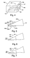
- Fig. 4 illustrates a perspective view of a solid body 180 that has been hollowed to form a wedge 150'.
- the wedge 150' is defined by the internally reflective surfaces 182, 184, 186, and 188 of the solid body 180 and the exit area 151'.
- the light source 102 may be located externally to the solid body 180 or may be fit into the solid body 180 flush with surface 182.
- the wedge extension element 154 has an entry face that is approximately the same dimensions as the exit face of the small wedge element 152.
- Fig. 2 illustrates a separation between the small wedge element 152 and the extension element 154 in the wedge 150 as a broken line 153 to indicate that the wedge 150 may be manufactured from one element or two (or more) elements.
- the extension element 154 may be formed of the same material as the small wedge element 152 or other material that has the desired optical properties, e.g., the same coefficient of refraction as the small wedge 152.
- the radiant intensity distribution of the light leaving the wedge extension element 154 is narrower than the distribution of the light entering the wedge extension element 154.
- the narrow distribution of light is particularly advantageous in a projection application because the optical system that is required to get the light from the light source to the target area can be greatly simplified if the light source has a narrow radiation pattern.
- an embodiment of the present invention includes a wedge 150 that extends laterally beyond the edge of the light source 102.
- the surface 155 of the wedge extends a distance D between the light source 102 and the exit surface 151.
- the surface 155 extends in a direction that is parallel to the face 103 of the light source 102.
- the portion of the surface 155 that is between the light source 102 and the exit surface 151 is covered with a reflective coating.
- the distance D may be greater than the width of the face 103 of the light source 102.
- the light source 102 may be a light emitting diode (LED), which includes a layer of first conductivity type 106 formed on a substrate 104.
- first conductivity type layer 106 may be an n-type III-nitride layer and substrate 104 may be sapphire, SiC, GaN, or any other suitable substrate.
- a light emitting region 108 also referred to as the active region, is formed on first conductivity type layer 106, then a layer of second conductivity type 112 is formed on active region 108.
- a first contact 114 is connected to first conductivity type layer 106 and a second contact 116 is connected to the second conductivity type layer 112. At least one of contacts 114 and 116 may be reflective.
- Interconnects 118 connect the light emitting diode to a submount 120 (shown in Fig. 3 ). Interconnects 118 may be, for example, solder bumps or gold bumps.
- the semiconductor layers in an LED are typically quite transparent to light at the emission wavelength.
- light rays 130 and 132 are transmitted through layers 108, 106 and 104 without absorption and are reflected off the reflective coating on the opposite wall of the wedge 150.
- the light rays may be reflected back through the LED 102, e.g., light ray 130 is reflected back through layers 104, 106, and 108 and is reflected off contacts 114 and 116.
- the light rays reflect off the sides of the wedge 150 until the light rays escape the wedge 150 through the exit surface 151.
- the wedge 150 prevents light from escaping the device 100 outside an area that matches the etendue-limit of the desired optical system.
- multiple light sources may be affixed to a wedge.
- light sources may be affixed to multiple sides of a wedge.
- Fig. 5 illustrates an embodiment, in which multiple light sources 202a, 202b, 202c are affixed to one side of a wedge 250, while additional light sources 202d, 202e, and 202f are affixed to another side of the wedge 250.
- the light sources may be LEDs similar to that described in reference to Fig. 2 .
- the light sources may be affixed to opposing sides of the wedge 250, or alternatively, may be affixed to non-opposing sides of the wedge 250.
- the portions of the wedge 250 not affixed to a light sources, other than the exit surface 251, may be coated with a reflective coating.
- the geometry of the wedge may vary.
- the wedge 150 may have planar sides and is thus, a planar wedge.
- the taper of the wedge may be non-linear, i.e., one or more sides of the wedge are non-planar and, thus, the wedge is non-planar.
- Fig. 6 illustrates an embodiment in which a portion of the wedge 280 has a convex shape.
- the wedge extension element 284 may have convex shape, while the small wedge element 282 is a planar wedge.
- a single element may be used and/or portions of the small wedge element 282 may also have a complex shape.
- Fig. 7 illustrates an embodiment that is similar to that shown in Fig. 6 , but a portion of the wedge 290, e.g., the wedge extension element 294, has a concave shape. As described above, if desired, a single element may be used and/or portions of the small wedge element 282 may also have a complex shape.
- the entire wedge or a portion of the wedge may have a parabolic or elliptical shape or a complex compound or faceted shape.
- FIG. 8 illustrates an illumination system 300 that includes the light source 102 and wedge 150 with a target area 350, which may be, e.g., a transparent microdisplay or other type of image panel, and no imaging optics are used.
- FIG. 9 illustrates an illumination system 360 that includes the light source 102 and wedge 150 with an imagining lens system 362 disposed between the wedge 150 and a target area 350.
- the radiation emitted by the wedge 350 is imaged onto the target area 350 using the imagining lens system 352. This is particularly advantageous as the dimensions of the exit surface 151 of the wedge 150 need not match the dimensions of the target area 354.
- the aspect ratio of the exit surface 151 of the wedge 150 can be matched to the aspect ratio of the target area, e.g., 4:3 for a standard television aspect ratio or 9:16 for a wide-screen application.
- Fig. 10 illustrates another embodiment of an illumination system 380 in which an integrator rod 382 is disposed between the exit surface 151 of the wedge 150 and the target area 350.
- the use of an integrator rod 382 may be used advantageously to make the light distribution more uniform.
- Fig. 11 illustrates a device 400 in which wavelength-converting material 402 is disposed between the small wedge element 152 and the wedge extension element 154.
- Material 402 may be, for example, a fluorescent material such as phosphor.
- the material 402 can be used to convert emitted blue radiation from the LED to a desired color.
- active region 108 of the light source 102 shown in Fig. 2
- material 402 may be a Ce-doped Yttrium Aluminum Garnet (YAG) phosphor, which absorbs blue emission and emits yellow light.
- YAG Ce-doped Yttrium Aluminum Garnet
- Yellow light from material 402 may mix with blue light from active region 108 such that the light that is emitted from the wedge extension element 154 appears as an intense white light source.
- the material 402 scatters the radiation.
- the wedge extension element 154 is used to collimate the radiation.
Landscapes
- Led Device Packages (AREA)
- Planar Illumination Modules (AREA)
- Led Devices (AREA)
Claims (9)
- Optisches System mit:zumindest einer ersten, Licht emittierende Diode (102; 202a-c);einem transparenten Element (150; 150') mit einer ersten Oberfläche (155; 162; 182), einer zweiten Oberfläche (168; 188) sowie einer Austrittsfläche (151; 151'), wobei die erste, Licht emittierende Diode auf der ersten Oberflüche des transparenten Elements angeordnet ist, wobei eine reflektive Beschichtung auf einem Teil der ersten Oberfläche des transparenten Elements zwischen der ersten, Licht emittierenden Diode und der Austrittsfläche des transparenten Elements angeordnet ist;wobei eine zweite, Licht emittierende Diode (202d-f) oder eine reflektive Beschichtung auf der zweiten Oberfläche (168) des transparenten Elements (150) angeordnet ist;wobei das transparente Element weiterhin umfasst:eine dritte Oberfläche (164; 184) sowieeine vierte Oberfläche (166; 186), die mit einem Material beschichtet ist, das von der ersten, Licht emittierenden Diode emittiertes Licht reflektiert;dadurch gekennzeichnet, dass das transparente Element so geformt ist, dass von zumindest der ersten, Licht emittierenden Diode (102; 202a-c) emittiertes Licht durch eine Reflexion von der reflektiven Beschichtung auf der ersten Oberfläche auf die Austrittsfläche des transparenten Elements gelenkt wird, und wobei ein Teil des Lichts durch Schichten (104, 106, 108) der ersten, Licht emittierenden Diode gelenkt wird und von mindestens einem Kontakt (114, 116) der ersten, Licht emittierenden Diode rückreflektiert wird, und wobei die erste und zweite Oberfläche des transparenten Elements einen Keil mit einer Spitze gegenüber der Austrittsfläche (151; 151') bilden und die dritte und vierte Oberfläche im Wesentlichen parallel verlaufen.
- Optisches System nach Anspruch 1, wobei die erste, Licht emittierende Diode (102; 202a-c) eine Oberfläche aufweist, die mit der ersten Oberfläche (155; 162; 182) des transparenten Elements (150; 150') gekoppelt ist, wobei die Oberfläche der ersten, Licht emittierenden Diode eine Breite aufweist, wobei der Teil der ersten Oberfläche (155; 162; 182) des transparenten Elements zwischen der ersten, Licht emittierenden Diode und der Austrittsfläche (151; 151') des transparenten Elements sich über eine Distanz (D) erstreckt, die größer als die Breite der Oberfläche der ersten Licht emittierenden Diode (102; 202a-c) ist.
- Optisches System nach Anspruch 1, wobei das transparente Element umfasst:ein erstes optisches Element (152), das mit der ersten, Licht emittierenden Diode (102) gekoppelt ist, wobei das erste optische Element eine Austrittsfläche (153) aufweist; sowieein zweites optisches Element (154) mit einer Eintrittsfläche, die mit der Austrittsfläche des ersten optischen Elements (152) gekoppelt ist, wobei das zweite optische Element eine Oberfläche aufweist, welche die Austrittsfläche (151) des transparenten Elements darstellt.
- Optisches System nach Anspruch 3, das weiterhin ein Wellenlängenumwandlungsmaterial (402) umfasst, das zwischen dem ersten optischen Element (152) und dem zweiten optischen Element (154) angeordnet ist.
- Optisches System nach Anspruch 1, wobei der Keil mindestens eine nichtplanare Oberfläche aufweist.
- Optisches System nach Anspruch 1, das weiterhin ein Image-Panel (350) umfasst, auf das von der Austrittsfläche (151) des transparenten Elements emittiertes Licht auffällt.
- Optisches System nach Anspruch 6, das weiterhin zumindest eine Linse (362) oder einen Integratorstab (382) umfasst, die/der zwischen dem Image-Panel und der Austrittsfläche (151) des transparenten Elements angeordnet ist.
- Optisches System nach Anspruch 1, das weiterhin mehrere Licht emittierende Dioden (202a-c) umfasst, die auf der ersten Oberfläche (155; 162; 182) des transparenten Elements angeordnet sind, wobei die reflektive Beschichtung auf dem Teil der ersten Oberfläche des transparenten Elements zwischen einer Licht emittierenden Diode (202a-c) und der Austrittsfläche (151; 151') des transparenten Elements vorgesehen ist.
- Optisches System nach Anspruch 1, wobei das transparente Element (150) aus der Gruppe, bestehend aus Saphir, Glas, Acryl und Silicon, ausgewählt wird.
Applications Claiming Priority (2)
| Application Number | Priority Date | Filing Date | Title |
|---|---|---|---|
| US765312 | 2004-01-26 | ||
| US10/765,312 US7080932B2 (en) | 2004-01-26 | 2004-01-26 | LED with an optical system to increase luminance by recycling emitted light |
Publications (2)
| Publication Number | Publication Date |
|---|---|
| EP1569283A1 EP1569283A1 (de) | 2005-08-31 |
| EP1569283B1 true EP1569283B1 (de) | 2013-03-13 |
Family
ID=34750425
Family Applications (1)
| Application Number | Title | Priority Date | Filing Date |
|---|---|---|---|
| EP05100195A Expired - Lifetime EP1569283B1 (de) | 2004-01-26 | 2005-01-14 | LED mit optischem System zum Erhöhen der Luminanz durch Recycling des ausgestrahlten Lichts |
Country Status (4)
| Country | Link |
|---|---|
| US (1) | US7080932B2 (de) |
| EP (1) | EP1569283B1 (de) |
| JP (1) | JP5150039B2 (de) |
| TW (1) | TWI383110B (de) |
Families Citing this family (84)
| Publication number | Priority date | Publication date | Assignee | Title |
|---|---|---|---|---|
| US7604378B2 (en) | 2003-07-02 | 2009-10-20 | S.C. Johnson & Son, Inc. | Color changing outdoor lights with active ingredient and sound emission |
| US7476002B2 (en) | 2003-07-02 | 2009-01-13 | S.C. Johnson & Son, Inc. | Color changing light devices with active ingredient and sound emission for mood enhancement |
| US7318659B2 (en) | 2004-03-03 | 2008-01-15 | S. C. Johnson & Son, Inc. | Combination white light and colored LED light device with active ingredient emission |
| US7484860B2 (en) | 2003-07-02 | 2009-02-03 | S.C. Johnson & Son, Inc. | Combination white light and colored LED light device with active ingredient emission |
| US7520635B2 (en) | 2003-07-02 | 2009-04-21 | S.C. Johnson & Son, Inc. | Structures for color changing light devices |
| US7503675B2 (en) | 2004-03-03 | 2009-03-17 | S.C. Johnson & Son, Inc. | Combination light device with insect control ingredient emission |
| AU2005219978B2 (en) | 2004-03-03 | 2010-08-26 | S.C. Johnson & Son, Inc. | LED light bulb with active ingredient emission |
| US7408201B2 (en) * | 2004-03-19 | 2008-08-05 | Philips Lumileds Lighting Company, Llc | Polarized semiconductor light emitting device |
| KR20070058380A (ko) * | 2004-04-23 | 2007-06-08 | 라이트 프리스크립션즈 이노베이터즈, 엘엘씨 | 발광 다이오드를 위한 광학 매니폴드 |
| US7380962B2 (en) * | 2004-04-23 | 2008-06-03 | Light Prescriptions Innovators, Llc | Optical manifold for light-emitting diodes |
| US7837348B2 (en) | 2004-05-05 | 2010-11-23 | Rensselaer Polytechnic Institute | Lighting system using multiple colored light emitting sources and diffuser element |
| CN1981157B (zh) * | 2004-05-05 | 2011-03-16 | 伦斯勒工业学院 | 使用固态发射器和降频转换材料的高效光源 |
| JP2008544553A (ja) * | 2005-06-23 | 2008-12-04 | レンセレイアー ポリテクニック インスティテュート | 短波長ledとダウンコンバージョン物質で白色光を生成するパッケージ設計 |
| US7499206B1 (en) * | 2005-12-09 | 2009-03-03 | Brian Edward Richardson | TIR light valve |
| WO2007081719A2 (en) | 2006-01-05 | 2007-07-19 | Illumitex, Inc. | Separate optical device for directing light from an led |
| TW200743223A (en) * | 2006-05-01 | 2007-11-16 | Coretronic Corp | Light-emitting diode light source system |
| US20070257271A1 (en) * | 2006-05-02 | 2007-11-08 | 3M Innovative Properties Company | Led package with encapsulated converging optical element |
| US7525126B2 (en) | 2006-05-02 | 2009-04-28 | 3M Innovative Properties Company | LED package with converging optical element |
| US20070257270A1 (en) * | 2006-05-02 | 2007-11-08 | 3M Innovative Properties Company | Led package with wedge-shaped optical element |
| US7390117B2 (en) * | 2006-05-02 | 2008-06-24 | 3M Innovative Properties Company | LED package with compound converging optical element |
| US7953293B2 (en) * | 2006-05-02 | 2011-05-31 | Ati Technologies Ulc | Field sequence detector, method and video device |
| US7740387B2 (en) * | 2006-05-24 | 2010-06-22 | 3M Innovative Properties Company | Backlight wedge with side mounted light source |
| US7660509B2 (en) | 2006-05-24 | 2010-02-09 | 3M Innovative Properties Company | Backlight asymmetric light input wedge |
| US7317182B2 (en) * | 2006-05-24 | 2008-01-08 | 3M Innovative Properties Company | Backlight wedge with encapsulated light source |
| US7607814B2 (en) * | 2006-05-24 | 2009-10-27 | 3M Innovative Properties Company | Backlight with symmetric wedge shaped light guide input portion with specular reflective surfaces |
| JP2009540616A (ja) * | 2006-06-12 | 2009-11-19 | スリーエム イノベイティブ プロパティズ カンパニー | 再発光半導体構造物を有するled装置及び集束光学要素 |
| US20080123343A1 (en) * | 2006-06-23 | 2008-05-29 | Tatsuru Kobayashi | Light source device, image display device, optical element and manufacturing method thereof |
| WO2008011377A2 (en) * | 2006-07-17 | 2008-01-24 | 3M Innovative Properties Company | Led package with converging extractor |
| US7703942B2 (en) * | 2006-08-31 | 2010-04-27 | Rensselaer Polytechnic Institute | High-efficient light engines using light emitting diodes |
| US9028087B2 (en) | 2006-09-30 | 2015-05-12 | Cree, Inc. | LED light fixture |
| US9222632B2 (en) | 2013-01-31 | 2015-12-29 | Cree, Inc. | LED lighting fixture |
| US9212812B2 (en) | 2013-02-11 | 2015-12-15 | Cree, Inc. | LED light fixture with integrated light shielding |
| US20090086491A1 (en) | 2007-09-28 | 2009-04-02 | Ruud Lighting, Inc. | Aerodynamic LED Floodlight Fixture |
| US7686469B2 (en) | 2006-09-30 | 2010-03-30 | Ruud Lighting, Inc. | LED lighting fixture |
| US8087960B2 (en) | 2006-10-02 | 2012-01-03 | Illumitex, Inc. | LED system and method |
| JP2010508651A (ja) * | 2006-10-31 | 2010-03-18 | ティーアイアール テクノロジー エルピー | 光励起可能媒体を含む光源 |
| US7889421B2 (en) | 2006-11-17 | 2011-02-15 | Rensselaer Polytechnic Institute | High-power white LEDs and manufacturing method thereof |
| US7618163B2 (en) * | 2007-04-02 | 2009-11-17 | Ruud Lighting, Inc. | Light-directing LED apparatus |
| DE102007019776A1 (de) * | 2007-04-26 | 2008-10-30 | Osram Opto Semiconductors Gmbh | Optoelektronisches Bauelement und Verfahren zur Herstellung einer Mehrzahl optoelektronischer Bauelemente |
| US8092042B2 (en) * | 2007-05-03 | 2012-01-10 | Ruud Lighting, Inc. | Shield member in LED apparatus |
| US20080289678A1 (en) * | 2007-05-25 | 2008-11-27 | Rouda Trace | Light recapturing system and method |
| DE102007053597A1 (de) * | 2007-11-09 | 2009-06-10 | Bausch & Lomb Inc. | Beleuchtungsvorrichtung, die eine erhöhte Strahldichte liefert |
| JP2011512037A (ja) | 2008-02-08 | 2011-04-14 | イルミテックス, インコーポレイテッド | エミッタ層成形のためのシステムおよび方法 |
| US7637630B2 (en) * | 2008-04-22 | 2009-12-29 | Ruud Lighting, Inc. | Integrated shield-gasket member in LED apparatus |
| US8348475B2 (en) | 2008-05-23 | 2013-01-08 | Ruud Lighting, Inc. | Lens with controlled backlight management |
| US8388193B2 (en) | 2008-05-23 | 2013-03-05 | Ruud Lighting, Inc. | Lens with TIR for off-axial light distribution |
| US9423096B2 (en) | 2008-05-23 | 2016-08-23 | Cree, Inc. | LED lighting apparatus |
| DE102008028886B4 (de) * | 2008-06-18 | 2024-02-29 | OSRAM Opto Semiconductors Gesellschaft mit beschränkter Haftung | Strahlungsemittierendes Bauelement und Verfahren zur Herstellung eines strahlungsemittierenden Bauelements |
| US7891835B2 (en) | 2008-07-15 | 2011-02-22 | Ruud Lighting, Inc. | Light-directing apparatus with protected reflector-shield and lighting fixture utilizing same |
| US7841750B2 (en) | 2008-08-01 | 2010-11-30 | Ruud Lighting, Inc. | Light-directing lensing member with improved angled light distribution |
| JP5226077B2 (ja) * | 2008-10-15 | 2013-07-03 | 株式会社小糸製作所 | 発光モジュール、発光モジュールの製造方法、および灯具ユニット |
| TW201034256A (en) | 2008-12-11 | 2010-09-16 | Illumitex Inc | Systems and methods for packaging light-emitting diode devices |
| US8152352B2 (en) * | 2009-01-02 | 2012-04-10 | Rambus International Ltd. | Optic system for light guide with controlled output |
| US8272770B2 (en) | 2009-01-02 | 2012-09-25 | Rambus International Ltd. | TIR switched flat panel display |
| US20100184616A1 (en) * | 2009-01-20 | 2010-07-22 | Bio-Rad Laboratories, Inc. | Spatially controlled illumination of biological sample array through wedge-shaped support |
| TWI398967B (zh) * | 2009-02-20 | 2013-06-11 | Lite On Electronics Guangzhou | 發光二極體晶片及其製法 |
| US9255686B2 (en) | 2009-05-29 | 2016-02-09 | Cree, Inc. | Multi-lens LED-array optic system |
| US8297818B2 (en) * | 2009-06-11 | 2012-10-30 | Rambus International Ltd. | Optical system with reflectors and light pipes |
| US20100315836A1 (en) * | 2009-06-11 | 2010-12-16 | Brian Edward Richardson | Flat panel optical display system with highly controlled output |
| US8152318B2 (en) * | 2009-06-11 | 2012-04-10 | Rambus International Ltd. | Optical system for a light emitting diode with collection, conduction, phosphor directing, and output means |
| DE102009037415A1 (de) * | 2009-08-13 | 2011-02-17 | Osram Opto Semiconductors Gmbh | Halbleiterlichtquelle |
| US8585253B2 (en) | 2009-08-20 | 2013-11-19 | Illumitex, Inc. | System and method for color mixing lens array |
| US8449128B2 (en) | 2009-08-20 | 2013-05-28 | Illumitex, Inc. | System and method for a lens and phosphor layer |
| CN102713421A (zh) * | 2009-11-18 | 2012-10-03 | 拉姆伯斯国际公司 | Led的内部收集反射器光学器件 |
| US9070851B2 (en) | 2010-09-24 | 2015-06-30 | Seoul Semiconductor Co., Ltd. | Wafer-level light emitting diode package and method of fabricating the same |
| US9263636B2 (en) * | 2011-05-04 | 2016-02-16 | Cree, Inc. | Light-emitting diode (LED) for achieving an asymmetric light output |
| TW201300702A (zh) | 2011-05-13 | 2013-01-01 | Rambus Inc | 照明組件 |
| US10408429B2 (en) | 2012-02-29 | 2019-09-10 | Ideal Industries Lighting Llc | Lens for preferential-side distribution |
| US9541257B2 (en) | 2012-02-29 | 2017-01-10 | Cree, Inc. | Lens for primarily-elongate light distribution |
| US9541258B2 (en) | 2012-02-29 | 2017-01-10 | Cree, Inc. | Lens for wide lateral-angle distribution |
| USD697664S1 (en) | 2012-05-07 | 2014-01-14 | Cree, Inc. | LED lens |
| US9435519B2 (en) | 2013-01-31 | 2016-09-06 | Cree, Inc. | Light-fixture support assembly |
| USD718490S1 (en) | 2013-03-15 | 2014-11-25 | Cree, Inc. | LED lens |
| TWI507639B (zh) * | 2013-06-03 | 2015-11-11 | Radiant Opto Electronics Corp | Light guide plate and lighting device |
| US9291340B2 (en) | 2013-10-23 | 2016-03-22 | Rambus Delaware Llc | Lighting assembly having n-fold rotational symmetry |
| US9523479B2 (en) | 2014-01-03 | 2016-12-20 | Cree, Inc. | LED lens |
| CN105849915B (zh) * | 2014-01-06 | 2019-04-02 | 亮锐控股有限公司 | 具有成形衬底的半导体发光器件和制造所述器件的方法 |
| JP6349904B2 (ja) * | 2014-04-18 | 2018-07-04 | 日亜化学工業株式会社 | 半導体発光装置およびその製造方法 |
| JP2016048718A (ja) * | 2014-08-27 | 2016-04-07 | 豊田合成株式会社 | 発光装置 |
| JP6428353B2 (ja) * | 2015-02-19 | 2018-11-28 | 日亜化学工業株式会社 | 発光装置 |
| JP6520373B2 (ja) * | 2015-05-14 | 2019-05-29 | 日亜化学工業株式会社 | 発光素子 |
| JP6414104B2 (ja) | 2016-02-29 | 2018-10-31 | 日亜化学工業株式会社 | 発光装置の製造方法 |
| CN205944139U (zh) | 2016-03-30 | 2017-02-08 | 首尔伟傲世有限公司 | 紫外线发光二极管封装件以及包含此的发光二极管模块 |
| US10468566B2 (en) | 2017-04-10 | 2019-11-05 | Ideal Industries Lighting Llc | Hybrid lens for controlled light distribution |
Citations (5)
| Publication number | Priority date | Publication date | Assignee | Title |
|---|---|---|---|---|
| GB2326023A (en) * | 1997-06-03 | 1998-12-09 | Hewlett Packard Co | Semiconductor light-emitting device |
| US6272269B1 (en) * | 1999-11-16 | 2001-08-07 | Dn Labs Inc. | Optical fiber/waveguide illumination system |
| US20030095399A1 (en) * | 2001-11-16 | 2003-05-22 | Christopher Grenda | Light emitting diode light bar |
| US6584714B1 (en) * | 1998-11-18 | 2003-07-01 | Bayer Aktiengesellschaft | Fluorescent, structured shaped bodies |
| WO2003056876A2 (en) * | 2001-12-14 | 2003-07-10 | Digital Optics International Corporation | Uniform illumination system |
Family Cites Families (18)
| Publication number | Priority date | Publication date | Assignee | Title |
|---|---|---|---|---|
| US3877052A (en) | 1973-12-26 | 1975-04-08 | Bell Telephone Labor Inc | Light-emitting semiconductor apparatus for optical fibers |
| US3968564A (en) | 1975-04-30 | 1976-07-13 | Northern Electric Company Limited | Alignment of optical fibers to light emitting diodes |
| JPS5753839A (en) | 1980-09-17 | 1982-03-31 | Matsushita Electric Ind Co Ltd | Optical reproducer |
| JP2759269B2 (ja) | 1988-07-29 | 1998-05-28 | 京セラ株式会社 | 発光素子 |
| US5359446A (en) | 1992-09-10 | 1994-10-25 | Eldec Corporation | Wide-angle, high-speed, free-space optical communications system |
| EP0683574B1 (de) | 1994-04-27 | 2003-03-19 | THOMSON multimedia | Optische Übertragungsanordnung mit mehreren Übertragungswegen |
| US5894196A (en) | 1996-05-03 | 1999-04-13 | Mcdermott; Kevin | Angled elliptical axial lighting device |
| JP4138017B2 (ja) * | 1997-02-19 | 2008-08-20 | ディジタル プロジェクション リミテッド | 照明システム |
| EP0881514A1 (de) | 1997-05-30 | 1998-12-02 | Lasag Ag | Optisches Koppelelement zur räumlichen Begrenzung und Homogenisierung eines Strahls mit grossem Öffnungswinkel |
| JP3448223B2 (ja) * | 1998-08-31 | 2003-09-22 | シャープ株式会社 | 光源装置 |
| JP2001085745A (ja) * | 1999-09-14 | 2001-03-30 | Toshiba Corp | 発光装置 |
| US6650377B2 (en) * | 2000-05-08 | 2003-11-18 | Colorlink, Inc. | Two panel projection systems |
| JP3760900B2 (ja) * | 2001-09-06 | 2006-03-29 | セイコーエプソン株式会社 | 導光装置、電気光学装置及び電子機器 |
| WO2003083530A1 (en) * | 2002-03-28 | 2003-10-09 | Koninklijke Philips Electronics N.V. | Compact lighting system and display device |
| JP4068387B2 (ja) * | 2002-04-23 | 2008-03-26 | 株式会社小糸製作所 | 光源ユニット |
| JP4135402B2 (ja) * | 2002-05-28 | 2008-08-20 | カシオ計算機株式会社 | 面光源 |
| US6730940B1 (en) | 2002-10-29 | 2004-05-04 | Lumileds Lighting U.S., Llc | Enhanced brightness light emitting device spot emitter |
| TWI224182B (en) * | 2003-01-02 | 2004-11-21 | Toppoly Optoelectronics Corp | Surface light source structure |
-
2004
- 2004-01-26 US US10/765,312 patent/US7080932B2/en not_active Expired - Lifetime
-
2005
- 2005-01-14 EP EP05100195A patent/EP1569283B1/de not_active Expired - Lifetime
- 2005-01-21 TW TW094101870A patent/TWI383110B/zh not_active IP Right Cessation
- 2005-01-25 JP JP2005016556A patent/JP5150039B2/ja not_active Expired - Fee Related
Patent Citations (5)
| Publication number | Priority date | Publication date | Assignee | Title |
|---|---|---|---|---|
| GB2326023A (en) * | 1997-06-03 | 1998-12-09 | Hewlett Packard Co | Semiconductor light-emitting device |
| US6584714B1 (en) * | 1998-11-18 | 2003-07-01 | Bayer Aktiengesellschaft | Fluorescent, structured shaped bodies |
| US6272269B1 (en) * | 1999-11-16 | 2001-08-07 | Dn Labs Inc. | Optical fiber/waveguide illumination system |
| US20030095399A1 (en) * | 2001-11-16 | 2003-05-22 | Christopher Grenda | Light emitting diode light bar |
| WO2003056876A2 (en) * | 2001-12-14 | 2003-07-10 | Digital Optics International Corporation | Uniform illumination system |
Also Published As
| Publication number | Publication date |
|---|---|
| TWI383110B (zh) | 2013-01-21 |
| JP5150039B2 (ja) | 2013-02-20 |
| US20050162849A1 (en) | 2005-07-28 |
| EP1569283A1 (de) | 2005-08-31 |
| US7080932B2 (en) | 2006-07-25 |
| JP2005210132A (ja) | 2005-08-04 |
| TW200535369A (en) | 2005-11-01 |
Similar Documents
| Publication | Publication Date | Title |
|---|---|---|
| EP1569283B1 (de) | LED mit optischem System zum Erhöhen der Luminanz durch Recycling des ausgestrahlten Lichts | |
| US6730940B1 (en) | Enhanced brightness light emitting device spot emitter | |
| US8278841B2 (en) | Light emitting diode light engine | |
| US7543959B2 (en) | Illumination system with optical concentrator and wavelength converting element | |
| JP6964611B2 (ja) | 熱伝導性の蛍光取り出しドームを備えたレーザベース光源 | |
| US8104923B2 (en) | Light-emitting apparatus | |
| CN103988502B (zh) | 具有荧光材料元件的照明单元 | |
| US10324247B2 (en) | Optical device for producing high brightness light | |
| US20150124428A1 (en) | Lens Having An Internal Reflection Layer | |
| JP2000221596A (ja) | 投射型ディスプレイ用の光源 | |
| WO2017056468A1 (ja) | 光源装置および投光装置 | |
| KR101315083B1 (ko) | 고휘도 발광 다이오드 장치 | |
| US10290675B2 (en) | Light emitting diode module and method of forming a light emitting diode module | |
| EP3286593B1 (de) | Integrationskegel für eine beleuchtungsvorrichtung | |
| JP7046917B2 (ja) | 波長変換素子及び発光装置 | |
| KR101848842B1 (ko) | 레이저 조명 장치 | |
| JP2017224528A (ja) | 照明装置 | |
| JP2021190313A (ja) | 光変換装置および照明システム | |
| KR20160129448A (ko) | 레이저 조명 장치 |
Legal Events
| Date | Code | Title | Description |
|---|---|---|---|
| PUAI | Public reference made under article 153(3) epc to a published international application that has entered the european phase |
Free format text: ORIGINAL CODE: 0009012 |
|
| AK | Designated contracting states |
Kind code of ref document: A1 Designated state(s): AT BE BG CH CY CZ DE DK EE ES FI FR GB GR HU IE IS IT LI LT LU MC NL PL PT RO SE SI SK TR |
|
| AX | Request for extension of the european patent |
Extension state: AL BA HR LV MK YU |
|
| 17P | Request for examination filed |
Effective date: 20060228 |
|
| AKX | Designation fees paid |
Designated state(s): DE |
|
| 17Q | First examination report despatched |
Effective date: 20070209 |
|
| RAP1 | Party data changed (applicant data changed or rights of an application transferred) |
Owner name: PHILIPS LUMILEDS LIGHTING COMPANY LLC |
|
| REG | Reference to a national code |
Ref country code: DE Ref legal event code: R079 Ref document number: 602005038534 Country of ref document: DE Free format text: PREVIOUS MAIN CLASS: H01L0033000000 Ipc: H01L0033580000 |
|
| GRAP | Despatch of communication of intention to grant a patent |
Free format text: ORIGINAL CODE: EPIDOSNIGR1 |
|
| RIC1 | Information provided on ipc code assigned before grant |
Ipc: H01L 33/58 20100101AFI20120904BHEP |
|
| RIN1 | Information on inventor provided before grant (corrected) |
Inventor name: KEUPER, MATTHIJS, H. |
|
| GRAS | Grant fee paid |
Free format text: ORIGINAL CODE: EPIDOSNIGR3 |
|
| GRAA | (expected) grant |
Free format text: ORIGINAL CODE: 0009210 |
|
| AK | Designated contracting states |
Kind code of ref document: B1 Designated state(s): DE |
|
| REG | Reference to a national code |
Ref country code: DE Ref legal event code: R081 Ref document number: 602005038534 Country of ref document: DE Owner name: PHILIPS LIGHTING NORTH AMERICA CORPORATION, SO, US Free format text: FORMER OWNER: LUMILEDS LIGHTING U.S., LLC, SAN JOSE, CALIF., US |
|
| REG | Reference to a national code |
Ref country code: DE Ref legal event code: R096 Ref document number: 602005038534 Country of ref document: DE Effective date: 20130508 |
|
| PLBE | No opposition filed within time limit |
Free format text: ORIGINAL CODE: 0009261 |
|
| STAA | Information on the status of an ep patent application or granted ep patent |
Free format text: STATUS: NO OPPOSITION FILED WITHIN TIME LIMIT |
|
| 26N | No opposition filed |
Effective date: 20131216 |
|
| REG | Reference to a national code |
Ref country code: DE Ref legal event code: R097 Ref document number: 602005038534 Country of ref document: DE Effective date: 20131216 |
|
| REG | Reference to a national code |
Ref country code: DE Ref legal event code: R081 Ref document number: 602005038534 Country of ref document: DE Owner name: SIGNIFY NORTH AMERICA CORPORATION, SOMERSET, US Free format text: FORMER OWNER: PHILIPS LUMILEDS LIGHTING COMPANY, LLC, SAN JOSE, CALIF, US Ref country code: DE Ref legal event code: R081 Ref document number: 602005038534 Country of ref document: DE Owner name: SIGNIFY NORTH AMERICA CORPORATION, SOMERSET, US Free format text: FORMER OWNER: LUMILEDS LLC (N. D. GES. D. STAATES DELAWARE), SAN JOSE, CALIF., US Ref country code: DE Ref legal event code: R081 Ref document number: 602005038534 Country of ref document: DE Owner name: PHILIPS LIGHTING NORTH AMERICA CORPORATION, SO, US Free format text: FORMER OWNER: PHILIPS LUMILEDS LIGHTING COMPANY, LLC, SAN JOSE, CALIF, US Ref country code: DE Ref legal event code: R082 Ref document number: 602005038534 Country of ref document: DE Representative=s name: MEISSNER BOLTE PATENTANWAELTE RECHTSANWAELTE P, DE Ref country code: DE Ref legal event code: R081 Ref document number: 602005038534 Country of ref document: DE Owner name: PHILIPS LIGHTING NORTH AMERICA CORPORATION, SO, US Free format text: FORMER OWNER: LUMILEDS LLC (N. D. GES. D. STAATES DELAWARE), SAN JOSE, CALIF., US Ref country code: DE Ref legal event code: R081 Ref document number: 602005038534 Country of ref document: DE Owner name: PHILIPS LIGHTING NORTH AMERICA CORPORATION, SO, US Free format text: FORMER OWNER: PHILIPS LUMILEDS LIGHTING COMPANY,LLC, SAN JOSE, CALIF, US |
|
| REG | Reference to a national code |
Ref country code: DE Ref legal event code: R081 Ref document number: 602005038534 Country of ref document: DE Owner name: SIGNIFY NORTH AMERICA CORPORATION, SOMERSET, US Free format text: FORMER OWNER: PHILIPS ELECTRONICS NORTH AMERICA CORPORATION (N.D.GES.D. STAATES DELAWARE), ANDOVER, MASS., US Ref country code: DE Ref legal event code: R082 Ref document number: 602005038534 Country of ref document: DE Representative=s name: MEISSNER BOLTE PATENTANWAELTE RECHTSANWAELTE P, DE Ref country code: DE Ref legal event code: R081 Ref document number: 602005038534 Country of ref document: DE Owner name: PHILIPS LIGHTING NORTH AMERICA CORPORATION, SO, US Free format text: FORMER OWNER: PHILIPS ELECTRONICS NORTH AMERICA CORPORATION (N.D.GES.D. STAATES DELAWARE), ANDOVER, MASS., US |
|
| REG | Reference to a national code |
Ref country code: DE Ref legal event code: R084 Ref document number: 602005038534 Country of ref document: DE |
|
| REG | Reference to a national code |
Ref country code: DE Ref legal event code: R082 Ref document number: 602005038534 Country of ref document: DE Representative=s name: MEISSNER BOLTE PATENTANWAELTE RECHTSANWAELTE P, DE Ref country code: DE Ref legal event code: R081 Ref document number: 602005038534 Country of ref document: DE Owner name: SIGNIFY NORTH AMERICA CORPORATION, SOMERSET, US Free format text: FORMER OWNER: PHILIPS LIGHTING NORTH AMERICA CORPORATION, SOMERSET, N.J., US |
|
| P01 | Opt-out of the competence of the unified patent court (upc) registered |
Effective date: 20230421 |
|
| PGFP | Annual fee paid to national office [announced via postgrant information from national office to epo] |
Ref country code: DE Payment date: 20240328 Year of fee payment: 20 |
|
| REG | Reference to a national code |
Ref country code: DE Ref legal event code: R079 Ref document number: 602005038534 Country of ref document: DE Free format text: PREVIOUS MAIN CLASS: H01L0033580000 Ipc: H10H0020855000 |
|
| REG | Reference to a national code |
Ref country code: DE Ref legal event code: R071 Ref document number: 602005038534 Country of ref document: DE |