EP1569246A1 - Zinkoxidwiderstand und herstellungsverfahren dafür - Google Patents
Zinkoxidwiderstand und herstellungsverfahren dafür Download PDFInfo
- Publication number
- EP1569246A1 EP1569246A1 EP03812374A EP03812374A EP1569246A1 EP 1569246 A1 EP1569246 A1 EP 1569246A1 EP 03812374 A EP03812374 A EP 03812374A EP 03812374 A EP03812374 A EP 03812374A EP 1569246 A1 EP1569246 A1 EP 1569246A1
- Authority
- EP
- European Patent Office
- Prior art keywords
- oxide
- zinc
- bismuth
- single crystals
- boron
- Prior art date
- Legal status (The legal status is an assumption and is not a legal conclusion. Google has not performed a legal analysis and makes no representation as to the accuracy of the status listed.)
- Withdrawn
Links
Images




Classifications
-
- H—ELECTRICITY
- H01—ELECTRIC ELEMENTS
- H01C—RESISTORS
- H01C7/00—Non-adjustable resistors formed as one or more layers or coatings; Non-adjustable resistors made from powdered conducting material or powdered semi-conducting material with or without insulating material
- H01C7/10—Non-adjustable resistors formed as one or more layers or coatings; Non-adjustable resistors made from powdered conducting material or powdered semi-conducting material with or without insulating material voltage responsive, i.e. varistors
-
- H—ELECTRICITY
- H01—ELECTRIC ELEMENTS
- H01C—RESISTORS
- H01C7/00—Non-adjustable resistors formed as one or more layers or coatings; Non-adjustable resistors made from powdered conducting material or powdered semi-conducting material with or without insulating material
- H01C7/10—Non-adjustable resistors formed as one or more layers or coatings; Non-adjustable resistors made from powdered conducting material or powdered semi-conducting material with or without insulating material voltage responsive, i.e. varistors
- H01C7/105—Varistor cores
- H01C7/108—Metal oxide
- H01C7/112—ZnO type
Definitions
- the present invention relates to a zinc oxide resistor, and more particularly a varistor device structure for protecting an electric/electronic circuit from surge voltages, and a production method thereof.
- a zinc oxide varistor is provided as a polycrystalline zinc-oxide ceramics.
- the zinc oxide varistor has been produced by mixing zinc oxide powder, transition metal oxide powder and bismuth oxide powder, and burning the mixture at a high temperature, to form a polycrystalline body with a structure in which a bismuth oxide or the like is segregated in the boundaries between zinc oxide grains each containing a transition metal oxide dissolved therein in the form of a solid solution (see, for example, the following Non-Patent Publication 1).
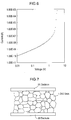
- an appropriate additive makes it possible for the zinc oxide ceramics to exhibit a nonlinear current-voltage characteristic in which each grain boundary in the zinc oxide ceramics has an operating voltage of about 3 V (see, for example, the following Non-Patent Publication 2). That is, the operating voltage as one of varistor characteristics is generally determined by the number of grain boundaries. Specifically, as shown in FIG 7, in a varistor device comprising two electrodes 2A, 2B provided at opposite end surfaces thereof and zinc oxide (ZnO) grains 1 residing therebetween, an overall operating voltage of the varistor device is determined by the product of the number of boundaries between the zinc oxide grains 1 and the operating voltage having the nonlinear current-voltage characteristic in each of the grain boundaries. Thus, the size of the zinc oxide grains 1 in the zinc oxide ceramics inherently contributes to the varistor characteristics.
- the grain size of a ceramics depends on an additive and a burning temperature, and generally has a statistical distribution. This causes difficulties in setting the number of grains or each size of grains in a ceramics at a predetermined value. Therefore, the production of a low-voltage type varistor essentially requires a particular technique in addition to a simple burning technique for forming a ceramics. For example, a varistor device having an operating voltage of 30 KV is required to ensure 10000 grain boundaries each having an operating voltage of 3 V. In contrast, a varistor device having an operating voltage of 6 V means a ceramics which includes 2 grain boundaries each having an operating voltage of 3 V, or only 3 grains. That is, some technique for forming a ceramics having a small number of grain boundaries is required to produce a varistor operable at a low voltage.
- This technique comprises preparing a sheet-shaped compact to be burned as a ceramics, and forming alternate layers of a metal electrode layer and a zinc-oxide ceramics layer, as shown in FIG. 8(A).
- the intervening metal layer makes it possible to hinder the contact between the zinc oxide grains or reduce the number of grain boundaries so as to achieve a varistor having a low operating voltage.
- each grain boundary of a zinc oxide varistor containing an appropriate additive has an operating voltage of 3 V.
- a low-voltage type varistor having any operating voltage of an integral multiple of 3 V can be produced by preparing a plurality of varistors each with a single grain boundary, and connecting them in series.
- Non-Patent Publications 4 includes a valuable suggestion that, while a nonlinear current-voltage characteristic is achieved by joining zinc-oxide single crystals each containing manganese and cobalt dissolved therein in the form of a solid solution, no nonlinear current-voltage characteristic is achieved if single crystals without addition of manganese and cobalt are joined together.
- the present invention provides a zinc oxide varistor having varistor characteristics achieved by a structure which comprises a pair of opposed zinc-oxide single crystals each containing cobalt and manganese dissolved therein in the form of a solid solution, and a glass layer forming an oxide grain boundary layer which includes a primary component consisting of bismuth and boron and intervenes between the zinc-oxide single crystals.
- the present invention provides a structure and production method for achieving zinc oxide varistor characteristics conventionally achieved in a zinc oxide sintered body, by a multilayer comprising a pair of opposed single crystals and a glass layer forming an oxide grain boundary layer.
- a conventional varistor consisting of polycrystalline body the technique of joining the opposed single crystals makes it possible to provide enhanced controllability of a resistor so as to obtain a varistor having an intended function.
- a pair of zinc-oxide single crystals containing cobalt and manganese dissolved therein in the form of a solid solution are joined together to form a joined unit so as to provide a nonlinear current-voltage characteristic in a resistor having the joined zinc-oxide single crystals.
- an intervening layer containing bismuth oxide is formed in the junction interface between the zinc-oxide single crystals to enhance the nonlinear current-voltage characteristic of the zinc oxide varistor.
- the grain boundary layer of the joined unit is formed of a bismuth-and-boron-containing oxide glass phase.
- the boron oxide added to the bismuth-containing layer residing in the junction interface can accelerate vitrification of the grain boundary layer by taking advantage of its feature of a low melting point.
- the zinc-oxide varistor or resistor has a current-voltage characteristic with significantly high nonlinearity, and a resistance value to be reduced in response to a high-voltage noise. Based on these features, the zinc-oxide resistor is used for protecting an electric/electronic circuit from an abnormal high voltage.
- the junction interface between the zinc-oxide single crystal/grain boundary layer/zinc-oxide single crystal distinctively provides significantly high nonlinearity at an operating voltage of about 3 V.
- the number of interfaces defined by the structure of (zinc-oxide single crystal/grain boundary layer/zinc-oxide single crystal) can be set at a desired value.
- the operating voltage for noise removal can be readily adjusted.
- a zinc oxide resistor of the present invention provides comprises as a basic unit a structure of (a zinc-oxide single crystal/a bismuth-boron based oxide interface layer/a zinc-oxide single crystal) formed of a pair of opposed zinc-oxide single crystals each containing cobalt and manganese dissolved therein in the form of a solid solution, and an oxide which contains a primary component consisting of bismuth and boron and intervenes between the zinc-oxide single crystals.
- the zinc oxide resistor has non-ohmic properties or exhibits zinc-oxide varistor characteristics, based on the intervening oxide interface layer, and the bismuth-boron based oxide interface layer is formed as a bismuth-and-boron-containing oxide glass phase by the action of the boron contained therein.
- FIG. 1 shows a nonlinear resistor which has the so-called "varistor characteristics", and a structure with only one grain boundary formed by joining a pair of opposed single crystals.
- the grain boundary is formed by disposing a pair of zinc-oxide single crystals 1A, 1B each containing cobalt and manganese dissolved therein in the form of a solid solution, in opposed relation to one another between a pair of electrodes 2A, 2B.
- the cobalt and manganese are elements which are considered to be essential to the expression of nonlinearity, as disclosed in the aforementioned Non-Patent Publication 4.
- the nonlinearity can be enhanced by segregating a grain boundary layer containing bismuth, in the grain boundary.
- an oxide layer 3 containing bismuth is provided as an interface layer disposed between the zinc-oxide single crystals 1A, 1B.
- the oxide layer 3 is formed as a glass phase containing bismuth oxide and boron oxide to provide enhanced junction strength.
- an auxiliary additive such as antimony
- an auxiliary additive such as antimony
- cobalt, manganese, bismuth and boron are used as additives in the zinc-oxide resistor structure of the present invention, it is to be understood that any other suitable auxiliary additive may be additionally used.
- the essence of the present invention lies in forming the bismuth-and-boron-containing oxide glass phase in the junction between the opposed zinc-oxide single crystals. Thus, it is not essential to the present invention whether an auxiliary additive other than cobalt and manganese is added to the opposed zinc-oxide single crystals.
- each of the opposed zinc-oxide single crystals may contain the cobalt dissolved therein in the form of a solid solution, in an amount of 0.5 mol% or more with respect to zinc therein.
- each of the opposed zinc-oxide single crystals preferably contains the cobalt dissolved therein in the form of a solid solution, in an amount of 0.5 mol% or more.
- an optimal cobalt concentration for achieving intended resistor characteristics is experimentally determined while taking account of the type and concentration of each impurity originally contained in zinc-oxide single crystals to be used.
- the solid solubility of cobalt into zinc oxide has a given limit, and the upper limit is determined by the solid solubility of the cobalt in the zinc oxide.
- each of the opposed zinc-oxide single crystals may contain the manganese dissolved therein in the form of a solid solution, in an amount of 0.05 mol% or more with respect to zinc therein.
- the addition of manganese can bring about an effect of reducing a leak current due to the grain boundary to provide enhanced nonlinearity.
- each of the opposed zinc-oxide single crystals may have a length of 5 mm, a width of 5 mm, and a thickness of 0.5 mm, and the oxide containing a primary component consisting of bismut
- the above composition of the interface layer is effective in producing the zinc oxide resistor using zinc-oxide single crystals prepared by cutting a commercially-available zinc-oxide single crystal having a typical thickness of 0.5 mm, into a size of 5 ⁇ 5 mm, to achieve excellent junction and nonlinearity.
- the present invention is not limited to the above composition, but any other suitable composition may be appropriately selected depending on the thickness of each zinc-oxide single crystal to be used, the type and quantity of element originally dissolved in the zinc-oxide single crystals to be joined, in the form of a solid solution, resistance characteristics required for the joined unit, and other factors. In the same manner, a temperature and/or time-period in the process of forming the junction may also be appropriately selected.
- the above zinc oxide resistor of the present invention comprising as a basic unit a structure of (a zinc-oxide single crystal/a bismuth-boron based oxide interface layer/a zinc-oxide single crystal) formed of a pair of opposed zinc-oxide single crystals each containing cobalt and manganese dissolved therein in the form of a solid solution, and an oxide which contains a primary component consisting of bismuth and boron and intervenes between the zinc-oxide single crystals, wherein the zinc oxide resistor has non-ohmic properties or exhibits zinc-oxide varistor characteristics, based on the intervening oxide interface layer, and the bismuth-boron based oxide interface layer is formed as a bismuth-and-boron-containing oxide glass phase by the action of the boron contained therein, (5) may exhibit an ⁇ -value of 20 or more, as a performance index of a zinc oxide varistor.
- the zinc oxide resistor has the opposed zinc-oxide single crystals containing the cobalt and manganese dissolved therein in a solid solution, and the grain boundary layer having the bismuth-and-boron-containing oxide glass phase and intervening in the joined unit.
- the zinc oxide resistor exhibits an ⁇ -value of 20 or more, as a performance index of a zinc oxide varistor.
- the above zinc oxide resistor of the present invention comprising as a basic unit a structure of (a zinc-oxide single crystal/a bismuth-boron based oxide interface layer/a zinc-oxide single crystal) formed of a pair of opposed zinc-oxide single crystals each containing cobalt and manganese dissolved therein in the form of a solid solution, and an oxide which contains a primary component consisting of bismuth and boron and intervenes between the zinc-oxide single crystals, wherein the zinc oxide resistor has non-ohmic properties or exhibits zinc-oxide varistor characteristics, based on the intervening oxide interface layer, and the bismuth-boron based oxide interface layer is formed as a bismuth-and-boron-containing oxide glass phase by the action of the boron contained therein, (6) the (zinc-oxide single crystal/bismuth-boron based oxide interface layer/zinc-oxide single crystal) structure serving as the basic unit may have an operating voltage of 2.9 ⁇ 0.3 V, as a
- the above zinc oxide resistor of the present invention comprising as a basic unit a structure of (a zinc-oxide single crystal/a bismuth-boron based oxide interface layer/a zinc-oxide single crystal) formed of a pair of opposed zinc-oxide single crystals each containing cobalt and manganese dissolved therein in the form of a solid solution, and an oxide which contains a primary component consisting of bismuth and boron and intervenes between the zinc-oxide single crystals, wherein the zinc oxide resistor has non-ohmic properties or exhibits zinc-oxide varistor characteristics, based on the intervening oxide interface layer, and the bismuth-boron based oxide interface layer is formed as a bismuth-and-boron-containing oxide glass phase by the action of the boron contained therein, (7) the (zinc-oxide single crystal/bismuth-boron based oxide interface layer/zinc-oxide single crystal) structure may be provided in a number of n.
- the structures of the number n may be repeatedly superimposed in a layered manner, and provided with a zinc-oxide single crystal superimposed thereon to form a (n + 1) layered structure including the number (n + 1) of zinc-oxide single crystals and the number n of bismuth-boron based oxide interface layers.
- the zinc-oxide resistor has an operating voltage of (2.9 ⁇ 0.3) n V, as a performance index of a zinc oxide varistor.
- the operating voltage of 2.9 ⁇ 0.3 V is achieved by a single junction, and the structures of the number n can be superimposed in a layered manner as shown in FIG. 2 to provide a multilayer zinc oxide resistor having any desired operating voltage.
- the above zinc oxide resistor of the present invention comprising as a basic unit a structure of (a zinc-oxide single crystal/a bismuth-boron based oxide interface layer/a zinc-oxide single crystal) formed of a pair of opposed zinc-oxide single crystals each containing cobalt and manganese dissolved therein in the form of a solid solution, and an oxide which contains a primary component consisting of bismuth and boron and intervenes between the zinc-oxide single crystals, wherein the zinc oxide resistor has non-ohmic properties or exhibits zinc-oxide varistor characteristics, based on the intervening oxide interface layer, and the bismuth-boron based oxide interface layer is formed as a bismuth-and-boron-containing oxide glass phase by the action of the boron contained therein, (8) the (zinc-oxide single crystal/bismuth-boron based oxide interface layer/zinc-oxide single crystal) structure may be adjusted to have an operating voltage of x V, as a performance index of a zinc
- the operating voltage of 2.9 ⁇ 0.3 V is achieved by a single junction, and the structures of the number n can be electrically connected to each other using lead wires as shown in FIG. 3 to provide a series-connected zinc oxide resistor having any desired operating voltage.
- a method of producing either one of the above zinc oxide resistors (1) to (7) of the present invention comprises: disposing an oxide containing bismuth and boron, between a pair of opposed zinc-oxide single crystals to form a sandwich structure of (a zinc-oxide single crystal/a composition to be formed as a glass phase/a zinc-oxide single crystal); heating and holding the sandwich structure at a high temperature allowing the oxide containing bismuth and boron, to be molten; and rapidly cooling the heated sandwich structure to join the pair of zinc-oxide single crystals with a glass-phase oxide interface layer intervening therebetween.
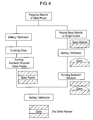
- a process of disposing the bismuth-and-boron-containing oxide between the opposed zinc-oxide single crystals, to form the sandwich structure of (a zinc-oxide single crystal/a composition to be formed as a glass phase/a zinc-oxide single crystal), includes a plurality of options.
- FIG. 4 shows this process.
- a suitable material for forming a desired glass phase is molten and vitrified in advance using a crucible, such as a platinum crucible, and then crushed to obtain a glass powder.
- a composition to be formed as a desired glass phase is placed on one zinc-oxide single crystal to be joined, and the zinc-oxide single crystal is used as a plate for vitrification without using a crucible.
- the obtained glass phase is disposed between a pair of zinc-oxide single crystals to be joined, and then they are subjected to a heat treatment to form a junction between the zinc-oxide single crystals.
- another zinc-oxide single crystal is disposed in opposed relation to the zinc-oxide single crystal having the vitrified composition attached thereon, and they are subjected to a heat treatment to form a junction between the zinc-oxide single crystals.
- a time-period of the heat treatment for heating the sandwich structure at a high temperature to melt the glass and form the junction is not limited to a specific value. While the heat-treatment time is required to set at a sufficient value for allowing the glass to be homogenized, an excessive heat-treatment time induces a reaction between the glass components and the zinc-oxide single crystals to cause elution of zinc oxide into the glass components. Thus, it is practically desirable to prepare a glass powder in advance as in the former case, and, after heating the glass powder at a high temperature allowing the glass to be molten, for a melting time of about 3 to 12 hours, rapidly cool the glass.
- the glass composition is preferably determined by synthesizing a glass phase containing bismuth and boron, melting and rapidly cooling the glass on the zinc-oxide single crystal to form a joined unit of zinc oxide and glass droplets, calculating a contact angle between the glass and the zinc-oxide single crystal based on this joined unit, selecting a glass allowing the contact angle to be 5 degrees or less.
- cobalt and manganese are added to the glass. If each of the zinc-oxide single crystals to be joined has a thin-plate shape, cobalt and manganese may be added in advance to glass components to be formed as the grain boundary of the joined unit, and diffused in the zinc-oxide single crystals in conjunction with the process of subjecting the sandwich structure to a heat treatment at a high temperature to melt the glass and form the junction.
- the heat treatment time for forming the junction is likely to cause insufficient diffusion of the cobalt and manganese from the molten glass to the zinc oxide.
- the above production method is preferably implemented in such a manner that a pair of zinc-oxide single crystals each containing cobalt and manganese diffused therein in advance is used together with the glass components to formed the sandwich structure, and then the sandwich structure is subjected to a heat treatment at a high temperature to form the junction.
- any other suitable method may be used to produce the above zinc oxide resistor comprising as a basic unit a structure of (a zinc-oxide single crystal/a bismuth-boron based oxide interface layer/a zinc-oxide single crystal) formed of a pair of opposed zinc-oxide single crystals each containing cobalt and manganese dissolved therein in the form of a solid solution, and an oxide which contains a primary component consisting of bismuth and boron and intervenes between the zinc-oxide single crystals, wherein the zinc oxide resistor has non-ohmic properties or exhibits zinc-oxide varistor characteristics, based on the intervening oxide interface layer, and the bismuth-boron based oxide interface layer is formed as a bismuth-and-boron-containing oxide glass phase by the action of the boron contained therein.
- the above zinc oxide resistor of the present invention comprising as a basic unit a structure of (a zinc-oxide single crystal/a bismuth-boron based oxide interface layer/a zinc-oxide single crystal) formed of a pair of opposed zinc-oxide single crystals each containing cobalt and manganese dissolved therein in the form of a solid solution, and an oxide which contains a primary component consisting of bismuth and boron and intervenes between the zinc-oxide single crystals, wherein the zinc oxide resistor has non-ohmic properties or exhibits zinc-oxide varistor characteristics, based on the intervening oxide interface layer, and the bismuth-boron based oxide interface layer is formed as a bismuth-and-boron-containing oxide glass phase by the action of the boron contained therein, is not limited by a production method thereof.
- a method of producing either one of the above zinc oxide resistors (1) to (7) of the present invention comprises: bringing each of two zinc-oxide single crystals into contact with a chunk of oxide cobalt, and heating the zinc-oxide single crystals and the chunk of oxide cobalt at a high temperature capable of inducing a diffusion reaction to diffuse cobalt from the chunk of oxide cobalt into the zinc-oxide single crystals so as to prepare a pair of zinc-oxide single crystals in such a manner as to have a cobalt concentration of 0.5 mol% or more; disposing an oxide containing bismuth and boron, between the pair of zinc-oxide single crystals disposed opposed to one another, to form a sandwich structure of (a zinc-oxide single crystal/a composition to be formed as a glass phase/a zinc-oxide single crystal); heating and holding the sandwich structure at a high temperature allowing the bismuth-and-boron-containing oxide to be molten; and rapidly cooling the heated sandwich structure to join the pair of zinc-
- the concentration of cobalt in the zinc-oxide single crystals to be joined is required to adjust the concentration of cobalt in the zinc-oxide single crystals to be joined, at a desired value.
- concentration of cobalt in the zinc-oxide single crystals to be joined it is required to introduce an appropriate amount of cobalt into the single crystal.
- cobalt can be conveniently introduced into a zinc-oxide single crystal by preparing a chunk containing a primary component consisting of oxide cobalt, bringing the chunk of oxide cobalt into contact with a target zinc-oxide single crystal, and heating and holding them at a high temperature.
- a measurement based on light absorption spectrum may be conveniently used for determining a quantity of cobalt to be introduced, in a nondestructive manner.
- an analytical curve may be made in advance to calculate a quantity of cobalt to be added, based on light absorption spectrum.
- the oxide containing a primary component consisting of bismuth and boron to be used for forming a junction between the opposed zinc-oxide single crystals, may be a glass prepared in such a manner as to contain, in oxide wt% equivalent, 37.0 to 22.7 wt% of B 2 O 3 , 3.8 to 1.9 wt% of Co 2 O 3 and 5.7 to 1.6 wt% of MnO 2 , with the remainder being bismuth oxide.
- each optimal quantity of cobalt, manganese, bismuth and boron to be contained in the glass phase differs depending on each size of the opposed zinc-oxide single crystals to be joined, and the type and quantity of additives originally containing therein.
- the above composition is simply shown as one example capable of producing a nonlinear resistor using the zinc-oxide single crystals each having a length of 5 mm, a width of 5 mm, and a thickness of 0.5 mm. Therefore, the above composition is not always an applicable value to all of zinc oxide resistors having the interface layer formed as a bismuth-and-boron-containing oxide glass phase according to the present invention.
- the oxide containing a primary component consisting of bismuth and boron, to be used for forming a junction between the opposed zinc-oxide single crystals may be a glass.
- the method may include flattening each surface of the opposed zinc-oxide single crystals through mirror polishing, and adjusting a quantity of the glass in such a manner that a molar ratio of the glass quantity in an equivalent bismuth quantity contained in the glass to a quantity of the opposed zinc-oxide single crystals, is set at 1.2 mol%.
- This total quantity of the glass phase for forming the junction simply shows a desirable value in one case where each surface of the opposed zinc-oxide single crystals is flatted through mirror polishing. Fundamentally, it is desirable that the total quantity of the glass phase for forming the junction is optimized in consideration of each flatness or surface area of the opposed zinc-oxide single crystals to be joined. Thus, in advance of an actual production, it is desirable to determine an optimal amount of bismuth with reference to the above recommended value.
- Each of two zinc-oxide single crystals was in contact with a cobalt-oxide sintered body, in an oxygen flow at 1200°C for 3 hours to diffuse cobalt into each zinc-oxide single crystal so as to prepare two cobalt-doped zinc-oxide single crystals.
- a quantity of the resulting solid solution of cobalt was calculated as about 1 at% based on optical spectrum.
- 0.8772 g of boron oxide, 8.8068 g of bismuth oxide, 0.1517g of cobalt oxide and 0.16431g of manganese oxide were measured and mixed together. The obtained mixture was put in a platinum crucible, and molten at 900°C in an oxygen flow.
- the molten mixture was flowed out of the crucible, and solidified to obtain a bismuth-and-boron-containing oxide glass.
- the obtained glass powder was dredged on one of the prepared cobalt-doped zinc-oxide single crystals (5 ⁇ 5 ⁇ 0.5 mm), and another zinc-oxide single crystal was superimposed on the single crystal with the glass powder to form a sandwich structure.
- the sandwich structure was heated at 1000°C in an oxygen flow for 12 hours, and then cooled to room temperature over a period of about 5 hours to produce a zinc oxide resistor.
- the manganese was dissolved in the zinc-oxide single crystals through diffusion.
- Each of two zinc-oxide single crystals was in contact with a cobalt-oxide sintered body, in an oxygen flow at 1200°C for 12 hours to diffuse cobalt into each zinc-oxide single crystal so as to prepare two cobalt-doped zinc-oxide single crystals. Then, 0.8772 g of boron oxide, 8.8068 g of bismuth oxide, 0.1517g of cobalt oxide and 0.16431g of manganese oxide were measured and mixed together. The obtained mixture was put in a platinum crucible, and molten at 900°C in an oxygen flow. Then, the molten mixture was flowed out of the crucible, and solidified to obtain a bismuth-and-boron-containing oxide glass.
- the obtained glass powder was dredged on one of the prepared cobalt-doped zinc-oxide single crystals (5 ⁇ 5 ⁇ 0.5 mm), and another zinc-oxide single crystal was superimposed on the single crystal with the glass powder to form a sandwich structure.
- the sandwich structure was heated at 1000°C in an oxygen flow for 4 hours, and then cooled to room temperature over a period of about 5 hours to produce a zinc oxide resistor.
- the manganese was dissolved in the zinc-oxide single crystals through diffusion.
- the obtained glass powder was dredged on one of two cobalt-doped zinc-oxide single crystals (5 ⁇ 5 ⁇ 0.5 mm) prepared in advance, and another zinc-oxide single crystal was superimposed on the single crystal with the glass powder to form a sandwich structure.
- the sandwich structure was heated at 1000°C in an oxygen flow for 1 hour, and then cooled to room temperature over a period of about 5 hours to produce a zinc oxide resistor. While a measurement about characteristics was attempted in the same manner as that in Incentive Examples 1 and 2, the zinc-oxide single crystals was peeled from one another during the measurement due to poor junction strength. The reason would be that the interface layer is formed as polycrystal due to no addition of boron into the interface layer, and consequently grain boundaries and/or cracks are formed in the interface layer to cause deterioration in mechanical strength.
- the sandwich structure was heated at 1000°C in an oxygen flow for 4 hours, and then cooled to room temperature over a period of about 5 hours to produce a zinc oxide resistor. While a measurement about characteristics was attempted in the same manner as that in Incentive Examples 1 and 2, a linear current-voltage characteristic was obtained without any observation of a nonlinear current-voltage characteristic
- the zinc oxide resistor of the present invention is applicable to a low-voltage varistor, and usable in removing low-voltage noises in electronic components.
Landscapes
- Engineering & Computer Science (AREA)
- Microelectronics & Electronic Packaging (AREA)
- Physics & Mathematics (AREA)
- Electromagnetism (AREA)
- Compositions Of Oxide Ceramics (AREA)
- Thermistors And Varistors (AREA)
Applications Claiming Priority (3)
| Application Number | Priority Date | Filing Date | Title |
|---|---|---|---|
| JP2002350574A JP3718702B2 (ja) | 2002-12-03 | 2002-12-03 | 酸化亜鉛抵抗体及びその製造法 |
| JP2002350574 | 2002-12-03 | ||
| PCT/JP2003/015448 WO2004051676A1 (ja) | 2002-12-03 | 2003-12-02 | 酸化亜鉛抵抗体及びその製造法 |
Publications (2)
| Publication Number | Publication Date |
|---|---|
| EP1569246A1 true EP1569246A1 (de) | 2005-08-31 |
| EP1569246A4 EP1569246A4 (de) | 2008-12-03 |
Family
ID=32463109
Family Applications (1)
| Application Number | Title | Priority Date | Filing Date |
|---|---|---|---|
| EP03812374A Withdrawn EP1569246A4 (de) | 2002-12-03 | 2003-12-02 | Zinkoxidwiderstand und herstellungsverfahren dafür |
Country Status (6)
| Country | Link |
|---|---|
| US (1) | US7362209B2 (de) |
| EP (1) | EP1569246A4 (de) |
| JP (1) | JP3718702B2 (de) |
| KR (1) | KR100668760B1 (de) |
| TW (1) | TWI301423B (de) |
| WO (1) | WO2004051676A1 (de) |
Families Citing this family (1)
| Publication number | Priority date | Publication date | Assignee | Title |
|---|---|---|---|---|
| TWI820611B (zh) * | 2022-02-23 | 2023-11-01 | 國立成功大學 | 氧化鋅變阻器材料、其製備方法及應用其之氧化鋅變阻器 |
Family Cites Families (8)
| Publication number | Priority date | Publication date | Assignee | Title |
|---|---|---|---|---|
| JPS6054761B2 (ja) * | 1979-01-16 | 1985-12-02 | 株式会社日立製作所 | 電圧非直線抵抗体 |
| US4400683A (en) * | 1981-09-18 | 1983-08-23 | Matsushita Electric Industrial Co., Ltd. | Voltage-dependent resistor |
| US4959262A (en) * | 1988-08-31 | 1990-09-25 | General Electric Company | Zinc oxide varistor structure |
| JP2536128B2 (ja) | 1989-02-20 | 1996-09-18 | 富士電機株式会社 | 電圧非直線抵抗素子の製造方法 |
| US5770113A (en) * | 1995-03-06 | 1998-06-23 | Matsushita Electric Industrial Co., Ltd. | Zinc oxide ceramics and method for producing the same |
| JPH10270214A (ja) | 1997-03-28 | 1998-10-09 | Toshiba Corp | 非直線抵抗体の積層接合体 |
| JPH11340009A (ja) * | 1998-05-25 | 1999-12-10 | Toshiba Corp | 非直線抵抗体 |
| JP2000228302A (ja) | 1999-02-04 | 2000-08-15 | Atsushi Iga | 酸化亜鉛系磁器積層物とその製造方法および酸化亜鉛バリスタ |
-
2002
- 2002-12-03 JP JP2002350574A patent/JP3718702B2/ja not_active Expired - Lifetime
-
2003
- 2003-12-02 WO PCT/JP2003/015448 patent/WO2004051676A1/ja not_active Ceased
- 2003-12-02 US US10/537,492 patent/US7362209B2/en not_active Expired - Fee Related
- 2003-12-02 EP EP03812374A patent/EP1569246A4/de not_active Withdrawn
- 2003-12-02 TW TW092133785A patent/TWI301423B/zh not_active IP Right Cessation
- 2003-12-02 KR KR1020057009922A patent/KR100668760B1/ko not_active Expired - Fee Related
Also Published As
| Publication number | Publication date |
|---|---|
| TWI301423B (en) | 2008-10-01 |
| US20060164200A1 (en) | 2006-07-27 |
| KR20050098835A (ko) | 2005-10-12 |
| JP2004186349A (ja) | 2004-07-02 |
| EP1569246A4 (de) | 2008-12-03 |
| WO2004051676A1 (ja) | 2004-06-17 |
| JP3718702B2 (ja) | 2005-11-24 |
| KR100668760B1 (ko) | 2007-01-12 |
| US7362209B2 (en) | 2008-04-22 |
| TW200413090A (en) | 2004-08-01 |
Similar Documents
| Publication | Publication Date | Title |
|---|---|---|
| EP0731065B1 (de) | Zinkoxidkeramiken und Verfahren zu ihrer Herstellung | |
| KR101152453B1 (ko) | 반도체 자기 조성물 | |
| DE69611642T2 (de) | Zinkoxidkeramik, Verfahren zu deren Herstellung und Zinkoxidvaristoren | |
| JP3822798B2 (ja) | 電圧非直線抵抗体及び磁器組成物 | |
| EP2966050A1 (de) | Halbleiterkeramikzusammensetzung und ptc-thermistor | |
| EP2305622B1 (de) | Varistormaterial mit hoher Feldstärke-Festigkeit | |
| RU2120146C1 (ru) | Композиция для электрического резистивного элемента, электрический резистивный элемент и способ его изготовления | |
| EP2585418B1 (de) | Kobaltfreie ntc-keramik und verfahren zur herstellung einer kobaltfreien ntc-keramik | |
| EP0803880B1 (de) | Spannungsabhängiger nichtlinearer Widerstand, Herstellungsverfahren und Überspannungsschutzelement | |
| EP0548394B1 (de) | Laminierter Halbleiterkeramikkondensator mit Zwischenkornisolation und Herstellungsverfahren | |
| US7305743B2 (en) | Method of producing piezoelectric ceramic device | |
| US7362209B2 (en) | Zinc oxide resistor and its manufacturing method | |
| KR20170066538A (ko) | 적층 코일 부품 | |
| EP0810611A1 (de) | Seltener metallhaltiger Hochtemperatur-Thermistor | |
| CN100590755C (zh) | 可变电阻素体和可变电阻 | |
| EP2393761B1 (de) | Varistorkeramik | |
| JP2004031436A (ja) | バリスタの製造方法 | |
| JPH0834136B2 (ja) | 電圧非直線抵抗体 | |
| CN111417608A (zh) | 陶瓷构件 | |
| JP2625178B2 (ja) | バリスタの製造方法 | |
| JP2008100856A (ja) | 酸化亜鉛積層チップバリスタの製造方法 | |
| JP2531586B2 (ja) | 電圧非直線抵抗体 | |
| JPH02184552A (ja) | 電圧非直線抵抗体用磁器組成物 | |
| JP2962056B2 (ja) | 電圧非直線抵抗体 | |
| JP2006245111A (ja) | ビスマス系酸化亜鉛バリスタ |
Legal Events
| Date | Code | Title | Description |
|---|---|---|---|
| PUAI | Public reference made under article 153(3) epc to a published international application that has entered the european phase |
Free format text: ORIGINAL CODE: 0009012 |
|
| 17P | Request for examination filed |
Effective date: 20050620 |
|
| AK | Designated contracting states |
Kind code of ref document: A1 Designated state(s): AT BE BG CH CY CZ DE DK EE ES FI FR GB GR HU IE IT LI LU MC NL PT SE SI SK TR |
|
| RBV | Designated contracting states (corrected) |
Designated state(s): DE FR |
|
| A4 | Supplementary search report drawn up and despatched |
Effective date: 20081030 |
|
| RIC1 | Information provided on ipc code assigned before grant |
Ipc: H01C 7/112 20060101AFI20081024BHEP |
|
| 17Q | First examination report despatched |
Effective date: 20091015 |
|
| STAA | Information on the status of an ep patent application or granted ep patent |
Free format text: STATUS: THE APPLICATION IS DEEMED TO BE WITHDRAWN |
|
| 18D | Application deemed to be withdrawn |
Effective date: 20100226 |