EP1566882A1 - Differenzoszillator - Google Patents
Differenzoszillator Download PDFInfo
- Publication number
- EP1566882A1 EP1566882A1 EP05250544A EP05250544A EP1566882A1 EP 1566882 A1 EP1566882 A1 EP 1566882A1 EP 05250544 A EP05250544 A EP 05250544A EP 05250544 A EP05250544 A EP 05250544A EP 1566882 A1 EP1566882 A1 EP 1566882A1
- Authority
- EP
- European Patent Office
- Prior art keywords
- oscillator
- bias
- differential
- bias voltage
- circuit according
- Prior art date
- Legal status (The legal status is an assumption and is not a legal conclusion. Google has not performed a legal analysis and makes no representation as to the accuracy of the status listed.)
- Withdrawn
Links
- 238000000034 method Methods 0.000 claims description 5
- 239000013078 crystal Substances 0.000 claims description 3
- 239000003990 capacitor Substances 0.000 claims description 2
- 230000000694 effects Effects 0.000 description 5
- 230000010355 oscillation Effects 0.000 description 4
- 230000008901 benefit Effects 0.000 description 2
- 230000001934 delay Effects 0.000 description 1
- 238000002955 isolation Methods 0.000 description 1
- 230000001960 triggered effect Effects 0.000 description 1
Images



Classifications
-
- H—ELECTRICITY
- H03—ELECTRONIC CIRCUITRY
- H03L—AUTOMATIC CONTROL, STARTING, SYNCHRONISATION OR STABILISATION OF GENERATORS OF ELECTRONIC OSCILLATIONS OR PULSES
- H03L3/00—Starting of generators
-
- H—ELECTRICITY
- H03—ELECTRONIC CIRCUITRY
- H03B—GENERATION OF OSCILLATIONS, DIRECTLY OR BY FREQUENCY-CHANGING, BY CIRCUITS EMPLOYING ACTIVE ELEMENTS WHICH OPERATE IN A NON-SWITCHING MANNER; GENERATION OF NOISE BY SUCH CIRCUITS
- H03B5/00—Generation of oscillations using amplifier with regenerative feedback from output to input
- H03B5/08—Generation of oscillations using amplifier with regenerative feedback from output to input with frequency-determining element comprising lumped inductance and capacitance
- H03B5/12—Generation of oscillations using amplifier with regenerative feedback from output to input with frequency-determining element comprising lumped inductance and capacitance active element in amplifier being semiconductor device
- H03B5/1206—Generation of oscillations using amplifier with regenerative feedback from output to input with frequency-determining element comprising lumped inductance and capacitance active element in amplifier being semiconductor device using multiple transistors for amplification
- H03B5/1218—Generation of oscillations using amplifier with regenerative feedback from output to input with frequency-determining element comprising lumped inductance and capacitance active element in amplifier being semiconductor device using multiple transistors for amplification the generator being of the balanced type
-
- H—ELECTRICITY
- H03—ELECTRONIC CIRCUITRY
- H03B—GENERATION OF OSCILLATIONS, DIRECTLY OR BY FREQUENCY-CHANGING, BY CIRCUITS EMPLOYING ACTIVE ELEMENTS WHICH OPERATE IN A NON-SWITCHING MANNER; GENERATION OF NOISE BY SUCH CIRCUITS
- H03B5/00—Generation of oscillations using amplifier with regenerative feedback from output to input
- H03B5/08—Generation of oscillations using amplifier with regenerative feedback from output to input with frequency-determining element comprising lumped inductance and capacitance
- H03B5/12—Generation of oscillations using amplifier with regenerative feedback from output to input with frequency-determining element comprising lumped inductance and capacitance active element in amplifier being semiconductor device
- H03B5/1231—Generation of oscillations using amplifier with regenerative feedback from output to input with frequency-determining element comprising lumped inductance and capacitance active element in amplifier being semiconductor device the amplifier comprising one or more bipolar transistors
-
- H—ELECTRICITY
- H03—ELECTRONIC CIRCUITRY
- H03B—GENERATION OF OSCILLATIONS, DIRECTLY OR BY FREQUENCY-CHANGING, BY CIRCUITS EMPLOYING ACTIVE ELEMENTS WHICH OPERATE IN A NON-SWITCHING MANNER; GENERATION OF NOISE BY SUCH CIRCUITS
- H03B2200/00—Indexing scheme relating to details of oscillators covered by H03B
- H03B2200/003—Circuit elements of oscillators
- H03B2200/0038—Circuit elements of oscillators including a current mirror
Definitions
- the present invention relates to a differential oscillator circuit and a method of starting up such a circuit.
- the circuit is symmetric about an oscillator 2 so as to provide a bias voltage to either side of the oscillator 2.
- a bias control line 4 is operable to turn the circuit on and off.
- the two halves of the bias circuitry are connected by a common line 6 which is operative to turn on the bias to both sides of the oscillator 2.
- a method of starting up a differential oscillator circuit having bias circuitry for applying a bias voltage to first and second sides of an oscillator including:
- a differential oscillator circuit including:
- the oscillator is deliberately unbalanced at the power enable stage.
- the oscillator is given a push which means that a stable operating amplitude is achieved more quickly than when relying on random voltage artifacts.
- the bias circuitry has a generally symmetric form. However, by virtue of the present invention, this is controlled to provide the oscillator bias voltage to one side of the oscillator in advance of the other side. There is no intention of applying significant pre-stressing to the oscillator, but only to cause a natural asymmetric disturbance to start the oscillating as soon as possible.
- oscillator circuit applications such as with TDMA (time division multiple access) circuits
- the bias circuitry is divided into two halves, a first half for applying the bias voltage to the first side of the oscillator and a second half for applying the bias voltage to the second side of the oscillator.
- the differential operating circuit further includes control circuitry arranged to cause the second half to apply the bias voltage to the second side of the oscillator only after the first half has been applying the bias voltage to the first side of the oscillator for the delay period.
- the unsymmetrical bias is provided upon start-up so as to encourage the oscillator to reach its stable operating amplitude more quickly.
- the bias circuitry includes a switch arrangement for selectively connecting the first half and the second half, such that, when the first half applies the bias voltage to the first side of the oscillator and the switch arrangement connects the first half to the second half, the switch arrangement causes the second half to apply the bias voltage to the second side of the oscillator.
- the two halves of a differential oscillator would normally be connected together in such a manner that, when the first half applies the bias voltage to the oscillator, the second half naturally follows the first half.
- the switch arrangement By providing the switch arrangement to selectively isolate the second half from the first half, it is possible to control the first half to apply the bias voltage to the oscillator, whilst isolating the second half and preventing the second half from applying the bias voltage to the oscillator. In this way, the second half can be controlled to start applying the bias voltage to the oscillator after the first half has already been applying the bias voltage to the oscillator for the delay period.
- the differential oscillator circuit further includes a delay circuit for controlling the switch arrangement to connect the first half to the second half after the first half applies the bias voltage to the second side of the oscillator by the delay period.
- the delay circuit is used to control the switch arrangement.
- a bias control line can be provided connected to the first half for carrying a signal to which the first and second halves are responsive to apply the bias voltage to the first and second sides of the oscillator respectively, the switch arrangement selectively isolating the second half from the bias control line.
- the delay circuit could be used in any other manner for controlling the bias circuitry to delay applying the bias voltage to the second side of the oscillator until after the first side of the oscillator by the delay period.
- the delay circuit could be used directly to link the first and second halves. Alternatively, the first and second halves could be controlled independently with the delay circuit forming part of that control.
- the present invention is applicable to many types of oscillator within the differential oscillator circuit, for instance a tank circuit or a crystal oscillator.
- the delay period should not be too great.
- the delay period must be of sufficient duration to allow the bias levels in the half of the oscillator enabled first to reach the quiescent DC level. This delay depends on the particular circuit topology employed and the values of the components used. To all intents and purposes, a very short delay would have both halves biasing-up simultaneously.
- the delay period is an intended delay produced intentionally by the circuitry and not merely an effect caused by the tolerances and switching rates of the various components in the circuitry.
- the delay period could be as short as possible whilst still achieving the desired effect.
- the delay period is between 1 nano-second and 1 micro-second, in particular in the region of 500 nano-seconds. This is particularly useful for an oscillator having a period in the region of 38 nano-seconds.
- the delay period is preferably greater than the oscillator.
- the delay period can be of the order of 10 times the oscillator period.
- the start-up unsymmetrical bias of the present invention it is not necessary for the start-up unsymmetrical bias of the present invention to form significant pre-stressing of the oscillator.
- an integrated circuit including a differential oscillator circuit as defined above.
- the integrated circuit can be an integrated circuit for use as one of the chip set of a mobile telephone, for instance a transmitter and/or receiver integrated circuit.
- a mobile telephone including a differential oscillator circuit as defined above or an integrated circuit as defined above.
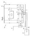
- the differential oscillator comprises bias circuitry 10 for applying an appropriate bias voltage to either side of an oscillator 12.
- the bias circuitry 10 is generally symmetric either side of the oscillator 12 in such a manner as to allow the oscillator 12 to oscillate as required.
- the bias circuitry can thus be considered as comprising a first half 10a on one side of the oscillator 12 and a second half 10b on the other side of the oscillator 12.
- the first half 10a is connected to a first side 12a of the oscillator 12 and the second side 10b is connected to a second side 12b of the oscillator 12.
- the oscillator 12 is embodied as a tank circuit. However, any form of an oscillator, such as a crystal oscillator, may be used.
- a bias control line 14 is connected to the bias circuitry 10.
- the bias control line 14 is used to carry a signal to control the differential oscillator.
- the bias circuitry 10 provides the appropriate bias to the oscillator 12.
- the particular components of the bias circuitry 10 illustrated in Figure 2 may be arranged in a known manner to do this and will be understood by the skilled reader.
- a line 16 connects the first half 10a of the bias circuitry to the second half 10b of the bias circuitry.
- the embodiment illustrated in Figure 2 includes a switch arrangement 18 which is controllable to selectively provide a break in the line 16 so as to disconnect the second half 10b from the first half 10a.
- the switch arrangement 18 may be embodied in any suitable manner according to the overall circuit design of the bias circuitry. However, as illustrated, the switching arrangement 18 includes two transistors, namely a main switching transistor 18a and a secondary earthing transistor 18b.
- the main switching transistor 18a is controllable to make or break a connection in the line 16.
- the secondary earthing transistor 18b is then provided to earth or connect to ground the line 16 on the side of the second half 10b when the main switching transistor 18a breaks the line 16 so as to disconnect the first half 10a from the second half 10b.
- control lines 20a and 20b are provided respectively to control the main switching transistor 18a and the secondary earthing transistor 18b.
- these control lines 20a and 20b carry respectively inverted control levels.
- the switching arrangement 18 can be used to keep the second half 10b of the bias circuitry isolated from the first half 10a and the line 16 at ground.
- the bias control line 14 is used to turn on the differential oscillator, only the first half 10a is activated to provide a bias to the oscillator 12.
- the first side 12a of the oscillator 12 is provided with the bias voltage, whereas the second side 12b of the oscillator 12 is kept at ground.
- the line 16 on the second half side of the bias circuitry 10 controls the second half 10b of the bias circuitry 10 to provide the bias voltage to the second side 12b of the oscillator 12.
- Switching of the switch arrangement 18 is arranged to take place at a time after the control bias line 14 activates the first half 10a of the bias circuitry 10, in particular after a delay period.
- the bias circuitry upon start-up, provides a large unsymmetrical bias across the oscillator.
- the circuit is deliberately unbalanced so as to provide a push across the oscillator 12 which brings the oscillator 12 to a stable operating amplitude more quickly than when relying on random circuit noise.
- the switch arrangement is controlled by means of a delay circuit 22 connected to the control lines 20a and 20b.
- the delay circuit 22 receives the signal of the bias control line 14 or an equivalent signal corresponding to it. Thus, when a signal is provided on the bias control line to start-up the differential oscillator, the delay circuit 22 is provided with a corresponding signal. However, the delay circuit 22 is arranged only to switch the switch arrangement after a delay period.
- the delay circuit 22 can include a capacitive element across which a voltage ramps up after the signal is provided to start-up the differential oscillator. According to the time constant of the resistive/capacitive circuit, the voltage across the capacitive element will reach a threshold after a predetermined period. After this delay period, the delay circuit can be triggered by the voltage reaching the threshold so as to operate the switch arrangement 18.
- the present invention is applicable to any differential oscillator.
- Figure 3 illustrates schematically a differential oscillator having an oscillator 12 with a first side 12a connected to a first half 10a of bias circuitry 10 and a second side 12b connected to a second half 10b of bias circuitry 10.
- a line 16 joins the first half 10a to the second half 10b such that the two halves 10a, 10b of the bias circuitry work simultaneously.
- Figure 4 illustrates schematically an arrangement corresponding to that described with reference to Figure 2.
- a bias control line 14 is used to actuate a first half 10a of the bias circuitry and also a delay circuit 22. After the delay period, the delay circuit 22 operates the switch arrangement 18 to connect the first half 10a to the second half 10b by means of the line 16.
- Figure 5 illustrates an embodiment having a control circuit 30 which includes a switch arrangement and a delay circuit.
- the control circuit 30 responds to a change in potential on the line 16a on the side of the first half 10a and, after the delay period, allows the same potential to develop on the line 16b on the side of the second half 10b.
- Figure 6 illustrates an arrangement where the first half 10a of the bias circuitry is controlled in effect independently of the second half 10b of the bias circuitry.
- a control circuit 40 actuates a bias control line 14a for the first half and a bias control line 14b for the second half 10b. It will be appreciated that the control circuit 40 provides the required signal on the second bias control line 14b after a delay period from providing a signal on the first bias control line 14a.
- Figure 7 illustrates an embodiment equivalent to those of Figures 2 and 4, but including a first capacitive element 50a connecting a first half 10a to the first side 12a of the oscillator 12 and a second capacitive element 50b connecting the second half 10b to the second side 12b of the oscillator 12.
- the capacitive elements 50a and 50b prevent any DC biassing of the oscillator 12. They will allow the unsymmetrical bias to be applied during start-up whilst preventing any substantial pre-stressing of the oscillator 12.
- the exact length of the delay period is not essential to the invention. The fact that there is a delay at all provides the unsymmetric bias and unbalancing to start oscillation. If the delay is too large, obviously the start-up time for the device is unnecessary extended. Clearly, if the delay becomes equal to the time taken by an "unassisted" oscillator to reach full oscillation amplitude, then there will be no benefit.
- the delay (max) value is difficult to quantify as it depends so much upon the exact circuitry employed.
- the delay period is in the region of 500 nano-seconds, but delays between 1 nano-second and 1 micro-second could be considered.
- the delay period is greater than the oscillator period, more preferably of the order of 10 times greater.
- differential oscillator circuit can be embodied in an integrated circuit as illustrated in Figure 8.
- differential oscillator circuit or the integrated circuit can be embodied in a mobile telephone such as illustrated in Figure 9.
Landscapes
- Oscillators With Electromechanical Resonators (AREA)
- Inductance-Capacitance Distribution Constants And Capacitance-Resistance Oscillators (AREA)
Applications Claiming Priority (2)
| Application Number | Priority Date | Filing Date | Title |
|---|---|---|---|
| GB0403609 | 2004-02-18 | ||
| GBGB0403609.1A GB0403609D0 (en) | 2004-02-18 | 2004-02-18 | Differential oscillator |
Publications (1)
| Publication Number | Publication Date |
|---|---|
| EP1566882A1 true EP1566882A1 (de) | 2005-08-24 |
Family
ID=32039964
Family Applications (1)
| Application Number | Title | Priority Date | Filing Date |
|---|---|---|---|
| EP05250544A Withdrawn EP1566882A1 (de) | 2004-02-18 | 2005-02-01 | Differenzoszillator |
Country Status (4)
| Country | Link |
|---|---|
| US (1) | US7187248B2 (de) |
| EP (1) | EP1566882A1 (de) |
| JP (1) | JP2005253069A (de) |
| GB (1) | GB0403609D0 (de) |
Families Citing this family (3)
| Publication number | Priority date | Publication date | Assignee | Title |
|---|---|---|---|---|
| JP4670496B2 (ja) * | 2005-06-14 | 2011-04-13 | 住友電気工業株式会社 | 光受信器 |
| JP4685060B2 (ja) * | 2006-06-08 | 2011-05-18 | パナソニック株式会社 | 差動発振装置 |
| US8427242B2 (en) * | 2009-01-15 | 2013-04-23 | Zebra Enterprises Solutions Corp. | Ultra wideband on-chip pulse generator |
Family Cites Families (3)
| Publication number | Priority date | Publication date | Assignee | Title |
|---|---|---|---|---|
| US5396195A (en) | 1993-12-13 | 1995-03-07 | At&T Corp. | Low-power-dissipation CMOS oscillator circuits |
| US6064277A (en) * | 1998-02-27 | 2000-05-16 | Analog Devices, Inc. | Automatic biasing scheme for reducing oscillator phase noise |
| EP1496609A1 (de) * | 2003-07-07 | 2005-01-12 | Dialog Semiconductor GmbH | Verbesserte Architekturen für spannungsgesteuerte Oszillatoren mit einzelnen Induktoren |
-
2004
- 2004-02-18 GB GBGB0403609.1A patent/GB0403609D0/en not_active Ceased
-
2005
- 2005-02-01 EP EP05250544A patent/EP1566882A1/de not_active Withdrawn
- 2005-02-17 US US11/059,855 patent/US7187248B2/en not_active Expired - Fee Related
- 2005-02-18 JP JP2005042760A patent/JP2005253069A/ja not_active Withdrawn
Non-Patent Citations (1)
| Title |
|---|
| KRAL A ET AL: "RF-CMOS oscillators with switched tuning", 11 May 1998, CUSTOM INTEGRATED CIRCUITS CONFERENCE, 1998. PROCEEDINGS OF THE IEEE 1998 SANTA CLARA, CA, USA 11-14 MAY 1998, NEW YORK, NY, USA,IEEE, US, PAGE(S) 555-558, ISBN: 0-7803-4292-5, XP010293959 * |
Also Published As
| Publication number | Publication date |
|---|---|
| JP2005253069A (ja) | 2005-09-15 |
| US20050179503A1 (en) | 2005-08-18 |
| US7187248B2 (en) | 2007-03-06 |
| GB0403609D0 (en) | 2004-03-24 |
Similar Documents
| Publication | Publication Date | Title |
|---|---|---|
| US7030709B2 (en) | Oscillator circuit with an inverter amplifier having reduced consumption | |
| KR100348002B1 (ko) | 발진기성능을개선시킨스위치가능한보상 | |
| US20030155954A1 (en) | Delay circuit with delay relatively independent of process, voltage, and temperature variations | |
| JPH05303449A (ja) | 零消費型パワーオンリセット回路 | |
| JP3284341B2 (ja) | 発振回路 | |
| JPH1117457A (ja) | 高速スタートアップ特性を備えた電子装置 | |
| JP2011118532A (ja) | 定電流回路 | |
| US8305153B2 (en) | Crystal oscillator with fast start-up and low current consumption | |
| JP2010087571A (ja) | 発振回路およびその制御方法 | |
| KR100483264B1 (ko) | 리얼 타임 클록의 저누설 배터리 동작용 cmos 회로 | |
| US7187248B2 (en) | Differential oscillator having two sides, an integrated circuit including the differential oscillator, a mobile telephone including the differential oscillator, and method of operating the differential oscillator | |
| KR20070066971A (ko) | 개시 클릭 노이즈를 제거할 수 있는 클래스 디 증폭기 | |
| EP0851323B1 (de) | Oszillatorschaltung, elektronische Schaltung damit, diese benutzende Halbleitervorrichtung, elektronisches Gerät und Uhrwerk | |
| US20080136541A1 (en) | Oscillator circuit | |
| KR100393536B1 (ko) | 전원회로 | |
| EP0685847B1 (de) | Niedrige Verlustleistungsinitialisierungsschaltung, insbesondere für Speicherregister | |
| JP3934189B2 (ja) | 水晶発振回路 | |
| US20240388253A1 (en) | Reducing Startup Time In A Crystal Oscillator | |
| JP2005191625A (ja) | 発振回路 | |
| JPH1032433A (ja) | 増幅器 | |
| JP2001511929A (ja) | クロックスイッチを有する電子回路 | |
| JPH11251836A (ja) | 温度補償型発振器 | |
| JP2004056472A (ja) | 発振回路 | |
| JPS63157509A (ja) | 信号発生装置 | |
| JP2006245817A (ja) | 電力増幅器 |
Legal Events
| Date | Code | Title | Description |
|---|---|---|---|
| PUAI | Public reference made under article 153(3) epc to a published international application that has entered the european phase |
Free format text: ORIGINAL CODE: 0009012 |
|
| AK | Designated contracting states |
Kind code of ref document: A1 Designated state(s): AT BE BG CH CY CZ DE DK EE ES FI FR GB GR HU IE IS IT LI LT LU MC NL PL PT RO SE SI SK TR |
|
| AX | Request for extension of the european patent |
Extension state: AL BA HR LV MK YU |
|
| 17P | Request for examination filed |
Effective date: 20051010 |
|
| AKX | Designation fees paid |
Designated state(s): DE FR GB |
|
| 17Q | First examination report despatched |
Effective date: 20061130 |
|
| GRAP | Despatch of communication of intention to grant a patent |
Free format text: ORIGINAL CODE: EPIDOSNIGR1 |
|
| RIC1 | Information provided on ipc code assigned before grant |
Ipc: H03L 3/00 20060101ALN20070712BHEP Ipc: H03B 5/12 20060101ALI20070712BHEP Ipc: H03B 5/06 20060101AFI20070712BHEP |
|
| STAA | Information on the status of an ep patent application or granted ep patent |
Free format text: STATUS: THE APPLICATION IS DEEMED TO BE WITHDRAWN |
|
| 18D | Application deemed to be withdrawn |
Effective date: 20071206 |