EP1566613A1 - Sensoreinrichtung - Google Patents
Sensoreinrichtung Download PDFInfo
- Publication number
- EP1566613A1 EP1566613A1 EP05002056A EP05002056A EP1566613A1 EP 1566613 A1 EP1566613 A1 EP 1566613A1 EP 05002056 A EP05002056 A EP 05002056A EP 05002056 A EP05002056 A EP 05002056A EP 1566613 A1 EP1566613 A1 EP 1566613A1
- Authority
- EP
- European Patent Office
- Prior art keywords
- binding material
- substrate
- sensor
- sensor device
- elasticity
- Prior art date
- Legal status (The legal status is an assumption and is not a legal conclusion. Google has not performed a legal analysis and makes no representation as to the accuracy of the status listed.)
- Ceased
Links
Images
Classifications
-
- G—PHYSICS
- G01—MEASURING; TESTING
- G01P—MEASURING LINEAR OR ANGULAR SPEED, ACCELERATION, DECELERATION, OR SHOCK; INDICATING PRESENCE, ABSENCE, OR DIRECTION, OF MOVEMENT
- G01P15/00—Measuring acceleration; Measuring deceleration; Measuring shock, i.e. sudden change of acceleration
- G01P15/02—Measuring acceleration; Measuring deceleration; Measuring shock, i.e. sudden change of acceleration by making use of inertia forces using solid seismic masses
- G01P15/08—Measuring acceleration; Measuring deceleration; Measuring shock, i.e. sudden change of acceleration by making use of inertia forces using solid seismic masses with conversion into electric or magnetic values
- G01P15/125—Measuring acceleration; Measuring deceleration; Measuring shock, i.e. sudden change of acceleration by making use of inertia forces using solid seismic masses with conversion into electric or magnetic values by capacitive pick-up
-
- G—PHYSICS
- G01—MEASURING; TESTING
- G01D—MEASURING NOT SPECIALLY ADAPTED FOR A SPECIFIC VARIABLE; ARRANGEMENTS FOR MEASURING TWO OR MORE VARIABLES NOT COVERED IN A SINGLE OTHER SUBCLASS; TARIFF METERING APPARATUS; MEASURING OR TESTING NOT OTHERWISE PROVIDED FOR
- G01D11/00—Component parts of measuring arrangements not specially adapted for a specific variable
- G01D11/24—Housings ; Casings for instruments
- G01D11/245—Housings for sensors
-
- G—PHYSICS
- G01—MEASURING; TESTING
- G01P—MEASURING LINEAR OR ANGULAR SPEED, ACCELERATION, DECELERATION, OR SHOCK; INDICATING PRESENCE, ABSENCE, OR DIRECTION, OF MOVEMENT
- G01P1/00—Details of instruments
- G01P1/02—Housings
- G01P1/023—Housings for acceleration measuring devices
-
- H—ELECTRICITY
- H10—SEMICONDUCTOR DEVICES; ELECTRIC SOLID-STATE DEVICES NOT OTHERWISE PROVIDED FOR
- H10W—GENERIC PACKAGES, INTERCONNECTIONS, CONNECTORS OR OTHER CONSTRUCTIONAL DETAILS OF DEVICES COVERED BY CLASS H10
- H10W72/00—Interconnections or connectors in packages
- H10W72/30—Die-attach connectors
-
- H—ELECTRICITY
- H10—SEMICONDUCTOR DEVICES; ELECTRIC SOLID-STATE DEVICES NOT OTHERWISE PROVIDED FOR
- H10W—GENERIC PACKAGES, INTERCONNECTIONS, CONNECTORS OR OTHER CONSTRUCTIONAL DETAILS OF DEVICES COVERED BY CLASS H10
- H10W72/00—Interconnections or connectors in packages
- H10W72/30—Die-attach connectors
- H10W72/321—Structures or relative sizes of die-attach connectors
- H10W72/325—Die-attach connectors having a filler embedded in a matrix
-
- H—ELECTRICITY
- H10—SEMICONDUCTOR DEVICES; ELECTRIC SOLID-STATE DEVICES NOT OTHERWISE PROVIDED FOR
- H10W—GENERIC PACKAGES, INTERCONNECTIONS, CONNECTORS OR OTHER CONSTRUCTIONAL DETAILS OF DEVICES COVERED BY CLASS H10
- H10W72/00—Interconnections or connectors in packages
- H10W72/30—Die-attach connectors
- H10W72/351—Materials of die-attach connectors
-
- H—ELECTRICITY
- H10—SEMICONDUCTOR DEVICES; ELECTRIC SOLID-STATE DEVICES NOT OTHERWISE PROVIDED FOR
- H10W—GENERIC PACKAGES, INTERCONNECTIONS, CONNECTORS OR OTHER CONSTRUCTIONAL DETAILS OF DEVICES COVERED BY CLASS H10
- H10W72/00—Interconnections or connectors in packages
- H10W72/30—Die-attach connectors
- H10W72/351—Materials of die-attach connectors
- H10W72/353—Materials of die-attach connectors not comprising solid metals or solid metalloids, e.g. ceramics
- H10W72/354—Materials of die-attach connectors not comprising solid metals or solid metalloids, e.g. ceramics comprising polymers
-
- H—ELECTRICITY
- H10—SEMICONDUCTOR DEVICES; ELECTRIC SOLID-STATE DEVICES NOT OTHERWISE PROVIDED FOR
- H10W—GENERIC PACKAGES, INTERCONNECTIONS, CONNECTORS OR OTHER CONSTRUCTIONAL DETAILS OF DEVICES COVERED BY CLASS H10
- H10W72/00—Interconnections or connectors in packages
- H10W72/851—Dispositions of multiple connectors or interconnections
- H10W72/874—On different surfaces
- H10W72/884—Die-attach connectors and bond wires
-
- H—ELECTRICITY
- H10—SEMICONDUCTOR DEVICES; ELECTRIC SOLID-STATE DEVICES NOT OTHERWISE PROVIDED FOR
- H10W—GENERIC PACKAGES, INTERCONNECTIONS, CONNECTORS OR OTHER CONSTRUCTIONAL DETAILS OF DEVICES COVERED BY CLASS H10
- H10W90/00—Package configurations
- H10W90/701—Package configurations characterised by the relative positions of pads or connectors relative to package parts
- H10W90/731—Package configurations characterised by the relative positions of pads or connectors relative to package parts of die-attach connectors
- H10W90/734—Package configurations characterised by the relative positions of pads or connectors relative to package parts of die-attach connectors between a chip and a stacked insulating package substrate, interposer or RDL
-
- H—ELECTRICITY
- H10—SEMICONDUCTOR DEVICES; ELECTRIC SOLID-STATE DEVICES NOT OTHERWISE PROVIDED FOR
- H10W—GENERIC PACKAGES, INTERCONNECTIONS, CONNECTORS OR OTHER CONSTRUCTIONAL DETAILS OF DEVICES COVERED BY CLASS H10
- H10W90/00—Package configurations
- H10W90/701—Package configurations characterised by the relative positions of pads or connectors relative to package parts
- H10W90/751—Package configurations characterised by the relative positions of pads or connectors relative to package parts of bond wires
- H10W90/754—Package configurations characterised by the relative positions of pads or connectors relative to package parts of bond wires between a chip and a stacked insulating package substrate, interposer or RDL
Definitions
- the present invention relates to a sensor device having a sensor chip and a bonding wire fixed by a binding material on a substrate used as a case, a circuit board or a lead frame.
- the acceleration sensor includes a sensor chip for sensing acceleration by a sensor portion disposed on a substrate made of silicon or the like, and a circuit chip as a base substrate mounting the sensor chip thereon by using an adhesive film.
- the sensor chip is connected to the substrate by a bonding wire. That is, the sensor chip is wire-bonded to the substrate.
- the conventional sensor device described above uses a binding material made of silicon resin or the like with minimum elasticity to protect the sensor chip fixed on the substrate from stress. In this manner, the sensitivity of the sensor device is improved.
- the modulus of elasticity of the binding material e.g. an adhesive film
- the modulus of elasticity of the binding material has to be 1 MPa or more in order to stably support the sensor chip when the wire is bonded on the chip.
- the sensitivity of the conventional sensor device is restricted by the modulus of elasticity of the binding material.
- the sensitivity of the sensor is restricted by the modulus of elasticity of the binding material.
- the less elastic binding material causes a problem in a wire bonding process. That is, the wire bonding process can't be stably conducted when the binding material is too low in the modulus of elasticity (too soft).
- a sensor device including a sensor chip and a bonding wire fixed on a substrate by a binding material suitable for both increased sensitivity and a wire bonding process.
- a sensor device of the present embodiment includes a sensor chip that is fixed on a substrate by a binding material and has a bonding wire connected thereto.
- a binding material that loses elasticity on application of energy in comparison to pre-energized state is used.
- the binding material is made less elastic when energized than in the pre-energized state.
- the binding material is elastic enough to stably support the sensor chip on the substrate for a wire bonding process in a pre-energized state.
- the binding material is then energized to be less elastic after the wire bonding process.
- the elasticity of the binding material becomes much lower than the one being used in the conventional art in terms of preventing stress transfer to the sensor chip.
- the sensor device having a sensor chip being fixed on a substrate by a binding material and having a bonding wire connected thereto can be wire-bonded and can also have an increased sensitivity.
- the binding material is has the following characteristics. That is, the energized binding material is functional as a cushion with air voids contained therein. In the energizing process, heat is used as a source of energy.
- the binding material is made of an adhesive containing a foaming agent that evaporates on application of heat.
- the binding material is heated to evaporate the foaming agent in the adhesive for forming air voids.
- the heated binding material becomes less elastic because of the air voids contained therein are functional as a cushion.
- the foaming agent is made of either of an Azodicarbonamide, a Di-nitrosopentamethylenetetramin, a Benzenesulphonyl hydrazide or a mixture of these materials.
- the acceleration sensor S1 may be implemented within, for example, a driving control system on an automotive vehicle, although the acceleration sensor is not necessarily limited to being implemented within such a device.
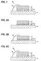
- a substrate 10 shown in FIG. 1 is a component such as a case, a housing, a printed circuit substrate/ceramic substrate or a lead frame may be utilized.
- a material for the substrate 10 may be, though not necessarily limited, resin, ceramic or metal.
- the case or the housing has a conducting portion to be connected to a bonding wire 40.
- the substrate 10 has a sensor chip 20 mounted thereon.
- the sensor chip 20 is attached to and fixed to the substrate 10 by a binding material 30.
- the sensor chip 20 and the substrate 10 are electrically connected by the bonding wire 40.
- the bonding wire 40 is formed in a wire bonding process that uses gold, aluminum or the like as a material of the bonding wire 40.
- the sensor chip 20 is, in this case, used as an acceleration sensor.
- a beam structure with a comb portion of well-known type is formed on a silicon substrate or the like to pick up changes of an interelectrode capacitance (electric signal) between a movable electrode and a fixed electrode being proportional to acceleration.
- the electric signal from the sensor chip 20 is, for example, converted by a C/V conversion circuit on the substrate 10 to variations of voltage, and then is output to an external circuit as an acceleration signal through the bonding wire 40 after being treated in processes such as amplification, adjustment and the like.
- the binding material 30 that attaches the sensor chip 20 to the substrate 10 is made of a material that reduces elasticity on an application of energy, such as heat, light or the like, while fixing the sensor chip 20 to the substrate 10, that is, while maintaining the functionality of an adhesive.
- the binding material 30 is already energized to have the modulus of elasticity of, for example, approximately 0.5 MPa, being much lower than a material used in a conventional sensor device.
- the binding material 30 is, as shown in FIG. 1, functional as a cushion because of voids 31 of air contained therein.
- the binding material of the conventional sensor device is homogeneous without any void contained therein, while the binding material 30 in the present embodiment is heterogeneous with the voids 31 contained therein to be functional as a cushion.
- the binding material 30 is made of, for example, an adhesive 32 containing a foaming agent 31 a that evaporates on application of heat (as shown in FIG. 2A).
- the binding material 30 of this kind contains the voids 31 when heat is applied to evaporate the foaming agent 31 a in the adhesive 32.
- the foaming agent 31 a in the binding material 30 is made of, for example, a material such as an Azodicarbonamide, a Di-nitrosopentamethylenetetramin, a Benzenesulphonyl hydrazide, a mixture of these materials or the like.
- the adhesive 32 is, for example, a thermosetting resin adhesive made of a silicon type resin with the modulus of elasticity of approximately 1 MPa.
- the foaming agent 31a is, for example, contained in the adhesive 32 as a powder.
- a mixture ratio having a preferable post-heating elasticity can be easily determined by those who are skilled in the art, based on the type and the elasticity of the adhesive 32.
- FIGS. 2A to 2C are schematical cross-sectional views of a manufacturing process of the acceleration sensor S1 illustrating how components are structured.
- the binding material 30 is placed on the substrate 10.
- the binding material 30 made of the adhesive 32 containing the powdered foaming agent 31 a is, as described above, applied to the substrate 10 by a dispense method or the like.
- the evaporative foaming agent 31 a on application of heat being made of a material such as an Azodicarbonamide, a Di-nitrosopentamethylenetetramin, a Benzenesulphonyl hydrazide or the like, is mixed in the silicon type adhesive 32 with the modulus of elasticity of 1 MPa.
- the sensor chip 20 is placed on the binding material 30, and is treated in a heating process and the like to harden the binding material 30.
- the adhesive 32 in the binding material 30 hardens while the foaming agent 31 a stays in a solid state (powder).
- the bonding wire 40 is bonded to the sensor chip 20 and the substrate 10 to electrically connect the chip 20 and the substrate 10.
- the foaming agent 31 a is still in a solid state (powder).
- the chip 20 fixed on the substrate by the binding material 30 is heated, for example, to 200°C.
- the foaming agent 31 a in the adhesive 32 evaporates and forms the voids 31. This completes the manufacturing process of the acceleration sensor S1 in this embodiment.
- the sensor device S1 including the sensor chip 20 being fixed on the substrate 10 by the binding material 30 and having the bonding wire 40 connected thereto, is characterized by the binding material 30 that reduces elasticity when energy is applied to the material 30.
- the binding material 30 fulfills the following requirements because the material 30 reduces elasticity when energy is applied. That is, the material 30 is elastic (hard enough) to stably support the sensor chip 20 fixed on the substrate 10 in the wire bonding process. The binding material 30 reduces elasticity after the wire bonding process on application of energy.
- the modulus of elasticity of the binding material 30 is 1 MPa or more in the wire bonding process, and the modulus of elasticity is reduced to approximately 0.5 MPa after the wire bonding process.
- the elasticity of the binding material 30 can be reduced to a level that is not sufficiently elastic (hard enough) to conduct the wire bonding. In other words, the elasticity of the binding material 30 can be lowered to an unprecedented level, thereby also lowering the stress transfer level to the sensor chip 20.
- the sensor chip 20 can be wire-bonded while sensitivity of the sensor device can be increased.
- the binding material 30 of the sensor device S1 in this embodiment is being functional as a cushion by containing the voids 31 of air as shown in FIG. 1.
- the binding material 30 is made of the silicon type adhesive 32 containing the foaming agent 31 a such as an Azodicarbonamide, a Di-nitrosopentamethylenetetramin, a Benzenesulphonyl hydrazide or a mixture of these materials to provide the required characteristics described above.
- the foaming agent 31 a such as an Azodicarbonamide, a Di-nitrosopentamethylenetetramin, a Benzenesulphonyl hydrazide or a mixture of these materials to provide the required characteristics described above.
- the above-described binding material 30 forms the voids 31 by evaporation of the foaming agent 31 a in the adhesive 32 on application of heat to the material 30 after the sensor chip 20 is fixed on and wire-bonded to the substrate 10.
- the binding material 30 preferably becomes heterogeneous and functional as a cushion after heating because of the voids 31 of air formed therein. As a result, the elasticity of the material 30 reduces.
- the extremely low elasticity of the binding material 30 required in this embodiment can only be achieved, for example, by using a gel type material when the material is homogeneous without voids as in the conventional art. In this case, the elasticity is too low to stably conduct a wire bonding process on a sensor chip.
- the foaming agent 31 a in the adhesive 32 evaporates on application of heat to form the voids 31.
- the voids 31 may also be formed by a light-sensitive foaming agent or the like.
- the binding material with an extremely low elasticity is provided by forming voids on application of heat or light.
- the binding material with this characteristic, reduction of elasticity on application of energy, is not necessarily provided in this manner.
- an adhesive that reduces elasticity on application of heat, light or the like, or an adhesive containing the material having that kind of characteristics may be used as the binding material.
- the binding material of the present embodiment is suitably prepared because the elasticity of the adhesive is reduced by a chemical reaction or the like to an extremely low level on application of energy (such as heat or the like).
- the binding material may also be made of an adhesive having an ingredient that evaporates or decomposes on application of heat, light or the like.
- the adhesive may include a material having this kind of characteristics as a mixture.
- the binding material of this kind will have spaces similar to voids formed by evaporation or decomposition on application of energy.
- the void-like space will be functional as a cushion in the binding material to appropriately provide the extremely low elasticity required in the present invention.
- the energy to be applied to the binding material may be, for example, an ultrasonic wave or the like.
- a binding material having a substance that decomposes on application of the ultrasonic wave will also be appropriately used in this embodiment.
- An acceleration sensor is taken as an example in the explanation of the present embodiment.
- the present embodiment may also be applied to other types of sensors, such as an angular velocity sensor, a pressure sensor, a temperature sensor or a light sensor. That is, the sensor chip 20 may be an angular velocity sensing element, a pressure sensing element, a temperature sensing element or a light sensing element in the embodiment described above.
Landscapes
- Physics & Mathematics (AREA)
- General Physics & Mathematics (AREA)
- Pressure Sensors (AREA)
- Adhesives Or Adhesive Processes (AREA)
Applications Claiming Priority (2)
| Application Number | Priority Date | Filing Date | Title |
|---|---|---|---|
| JP2004033087 | 2004-02-10 | ||
| JP2004033087A JP4337570B2 (ja) | 2004-02-10 | 2004-02-10 | センサ装置およびその製造方法 |
Publications (1)
| Publication Number | Publication Date |
|---|---|
| EP1566613A1 true EP1566613A1 (de) | 2005-08-24 |
Family
ID=34709075
Family Applications (1)
| Application Number | Title | Priority Date | Filing Date |
|---|---|---|---|
| EP05002056A Ceased EP1566613A1 (de) | 2004-02-10 | 2005-02-01 | Sensoreinrichtung |
Country Status (5)
| Country | Link |
|---|---|
| US (1) | US7223637B2 (de) |
| EP (1) | EP1566613A1 (de) |
| JP (1) | JP4337570B2 (de) |
| KR (1) | KR100682625B1 (de) |
| CN (1) | CN1654963A (de) |
Families Citing this family (7)
| Publication number | Priority date | Publication date | Assignee | Title |
|---|---|---|---|---|
| JP5045769B2 (ja) * | 2009-03-04 | 2012-10-10 | 株式会社デンソー | センサ装置の製造方法 |
| CN103983807B (zh) * | 2014-05-15 | 2018-06-22 | 清华大学 | 硅微机械加速度计 |
| KR102285332B1 (ko) | 2014-11-11 | 2021-08-04 | 삼성전자주식회사 | 반도체 패키지 및 이를 포함하는 반도체 장치 |
| KR102177621B1 (ko) * | 2014-12-30 | 2020-11-11 | 코오롱글로텍주식회사 | 원단용 입체 열전사 필름 |
| KR101775017B1 (ko) * | 2016-06-14 | 2017-09-05 | 세종공업 주식회사 | 다공성 접착제 제조방법 및 이에 의해 제조된 다공성 접착제가 사용된 가스센서 |
| JP7091696B2 (ja) | 2018-02-20 | 2022-06-28 | 株式会社デンソー | 物理量センサおよび半導体装置 |
| EP3929540A1 (de) * | 2020-06-26 | 2021-12-29 | TE Connectivity Norge AS | Befestigungssystem zur befestigung eines sensors an einem substrat, verfahren zur befestigung eines sensors an einem substrat |
Citations (6)
| Publication number | Priority date | Publication date | Assignee | Title |
|---|---|---|---|---|
| DE1569535A1 (de) * | 1961-10-21 | 1969-07-10 | Whiffen & Sons Ltd | Blaehmittelkombination und Verfahren zur Herstellung zellfoermiger Materialien |
| US5483106A (en) * | 1993-07-30 | 1996-01-09 | Nippondenso Co., Ltd. | Semiconductor device for sensing strain on a substrate |
| US20010031512A1 (en) * | 2000-03-16 | 2001-10-18 | Johann Winderl | Method and apparatus for applying a semiconductor chip to a carrier element |
| DE10130131A1 (de) * | 2000-06-26 | 2002-01-03 | Denso Corp | Dynamischer Halbleitersensor und Verfahren zu dessen Herstellung |
| US6486003B1 (en) * | 1996-12-13 | 2002-11-26 | Tessera, Inc. | Expandable interposer for a microelectronic package and method therefor |
| US20030006508A1 (en) * | 2001-07-06 | 2003-01-09 | Toshiya Ikezawa | Electronic device including stacked microchips |
Family Cites Families (6)
| Publication number | Priority date | Publication date | Assignee | Title |
|---|---|---|---|---|
| JPH0676790B2 (ja) | 1987-07-30 | 1994-09-28 | 株式会社東芝 | イグナイタ |
| US5001542A (en) | 1988-12-05 | 1991-03-19 | Hitachi Chemical Company | Composition for circuit connection, method for connection using the same, and connected structure of semiconductor chips |
| US6157085A (en) | 1998-04-07 | 2000-12-05 | Citizen Watch Co., Ltd. | Semiconductor device for preventing exfoliation from occurring between a semiconductor chip and a resin substrate |
| US6503780B1 (en) * | 2000-07-05 | 2003-01-07 | Amkor Technology, Inc. | Wafer scale image sensor package fabrication method |
| US6871395B2 (en) * | 2001-08-06 | 2005-03-29 | Siemens Technology-To-Business Center, Llc. | Methods for manufacturing a tactile sensor using an electrically conductive elastomer |
| TW200507279A (en) * | 2003-07-16 | 2005-02-16 | Adv Lcd Tech Dev Ct Co Ltd | Thin-film semiconductor substrate, method of manufacturing the same; apparatus for and method of crystallization;Thin-film semiconductor apparatus, method of manufacturing the same; |
-
2004
- 2004-02-10 JP JP2004033087A patent/JP4337570B2/ja not_active Expired - Fee Related
-
2005
- 2005-02-01 EP EP05002056A patent/EP1566613A1/de not_active Ceased
- 2005-02-01 KR KR1020050009188A patent/KR100682625B1/ko not_active Expired - Fee Related
- 2005-02-01 US US11/046,793 patent/US7223637B2/en not_active Expired - Fee Related
- 2005-02-07 CN CNA2005100070715A patent/CN1654963A/zh active Pending
Patent Citations (6)
| Publication number | Priority date | Publication date | Assignee | Title |
|---|---|---|---|---|
| DE1569535A1 (de) * | 1961-10-21 | 1969-07-10 | Whiffen & Sons Ltd | Blaehmittelkombination und Verfahren zur Herstellung zellfoermiger Materialien |
| US5483106A (en) * | 1993-07-30 | 1996-01-09 | Nippondenso Co., Ltd. | Semiconductor device for sensing strain on a substrate |
| US6486003B1 (en) * | 1996-12-13 | 2002-11-26 | Tessera, Inc. | Expandable interposer for a microelectronic package and method therefor |
| US20010031512A1 (en) * | 2000-03-16 | 2001-10-18 | Johann Winderl | Method and apparatus for applying a semiconductor chip to a carrier element |
| DE10130131A1 (de) * | 2000-06-26 | 2002-01-03 | Denso Corp | Dynamischer Halbleitersensor und Verfahren zu dessen Herstellung |
| US20030006508A1 (en) * | 2001-07-06 | 2003-01-09 | Toshiya Ikezawa | Electronic device including stacked microchips |
Non-Patent Citations (4)
| Title |
|---|
| "Encyclopedia of Polymer Science and Technology", 15 July 2004, JOHN WILEY & SONS, INC., article CHARLES E. CARRAHER: "Thermosets", pages: 209 - 227, XP055027425 * |
| RHOMIE L HECK III: "A review of commercially used chemical foaming agents for thermoplastic foams", JOURNAL OF VINYL TECHNOLOGY, MANCHESTER, NH, US, vol. 4, no. 2, 1 January 1998 (1998-01-01), pages 113 - 116, XP009129409, ISSN: 0193-7197 * |
| RHOMIE L. HECK ET AL: "Blowing Agents", ENCYCLOPEDIA OF POLYMER SCIENCE AND TECHNOLOGY, 15 February 2011 (2011-02-15), XP055027427, Retrieved from the Internet <URL:http://onlinelibrary.wiley.com/store/10.1002/0471440264.pst032/asset/pst032.pdf?v=1&t=h2a9uv53&s=5844312bc02ce7d450daa4a375223f3a62ce6823> [retrieved on 20120516], DOI: http://dx.doi.org/10.1002/0471440264.pst032 * |
| WIKIPEDIA: "Adhesive", INTERNET CITATION, 13 May 2012 (2012-05-13), pages 1 - 9, XP007920631, Retrieved from the Internet <URL:http://en.wikipedia.org/wiki/Adhesive> [retrieved on 20120516] * |
Also Published As
| Publication number | Publication date |
|---|---|
| US7223637B2 (en) | 2007-05-29 |
| JP2005228777A (ja) | 2005-08-25 |
| CN1654963A (zh) | 2005-08-17 |
| JP4337570B2 (ja) | 2009-09-30 |
| US20050173810A1 (en) | 2005-08-11 |
| KR100682625B1 (ko) | 2007-02-15 |
| KR20060042922A (ko) | 2006-05-15 |
Similar Documents
| Publication | Publication Date | Title |
|---|---|---|
| US6708564B2 (en) | Angular velocity measuring apparatus | |
| US20010055836A1 (en) | Semiconductor dynamic sensor and method of manufacturing the same | |
| US7223637B2 (en) | Method of manufacturing a sensor device with binding material having a foaming agent | |
| CN1537331A (zh) | 电路组件及其制造方法 | |
| US20060049497A1 (en) | Physical quantity sensor | |
| CN101057148A (zh) | 加速度传感器装置 | |
| JP2003021647A (ja) | 電子装置 | |
| US6313514B1 (en) | Pressure sensor component | |
| US5751059A (en) | Pyroelectric sensor | |
| JP2006153799A (ja) | 角速度センサ装置およびその製造方法 | |
| US20050199988A1 (en) | Sensor device | |
| JPH06207870A (ja) | 半導体圧力センサ | |
| JPH04348280A (ja) | ヒータ内蔵ハイブリッドic | |
| JP3241385B2 (ja) | 電子部品およびそのパッケージ内への装着方法 | |
| JPH07263618A (ja) | 混成集積回路装置 | |
| JP2668995B2 (ja) | 半導体装置 | |
| JPH11230846A (ja) | 半導体力学量センサの製造方法 | |
| JP3443522B2 (ja) | 光半導体素子収納用パッケージ | |
| JPH06307950A (ja) | 歪センサ | |
| JPH01282846A (ja) | 混成集積回路 | |
| JP3426726B2 (ja) | 半導体素子収納用パッケージ | |
| JPS6125222B2 (de) | ||
| JP2765265B2 (ja) | 半導体装置用リードフレーム | |
| JP2009130235A (ja) | 圧電デバイスとこれを用いた電子機器、及び自動車 | |
| JPH10229102A (ja) | 電子製品 |
Legal Events
| Date | Code | Title | Description |
|---|---|---|---|
| PUAI | Public reference made under article 153(3) epc to a published international application that has entered the european phase |
Free format text: ORIGINAL CODE: 0009012 |
|
| AK | Designated contracting states |
Kind code of ref document: A1 Designated state(s): AT BE BG CH CY CZ DE DK EE ES FI FR GB GR HU IE IS IT LI LT LU MC NL PL PT RO SE SI SK TR |
|
| AX | Request for extension of the european patent |
Extension state: AL BA HR LV MK YU |
|
| 17P | Request for examination filed |
Effective date: 20050905 |
|
| AKX | Designation fees paid |
Designated state(s): DE FR GB |
|
| 17Q | First examination report despatched |
Effective date: 20061020 |
|
| STAA | Information on the status of an ep patent application or granted ep patent |
Free format text: STATUS: THE APPLICATION HAS BEEN REFUSED |
|
| 18R | Application refused |
Effective date: 20120510 |