EP1559739A1 - Dispersions and films comprising conducting polymer for optoelectronic devices - Google Patents
Dispersions and films comprising conducting polymer for optoelectronic devices Download PDFInfo
- Publication number
- EP1559739A1 EP1559739A1 EP20050000280 EP05000280A EP1559739A1 EP 1559739 A1 EP1559739 A1 EP 1559739A1 EP 20050000280 EP20050000280 EP 20050000280 EP 05000280 A EP05000280 A EP 05000280A EP 1559739 A1 EP1559739 A1 EP 1559739A1
- Authority
- EP
- European Patent Office
- Prior art keywords
- film
- dispersion
- conductivity
- layer
- conducting polymer
- Prior art date
- Legal status (The legal status is an assumption and is not a legal conclusion. Google has not performed a legal analysis and makes no representation as to the accuracy of the status listed.)
- Withdrawn
Links
- 239000006185 dispersion Substances 0.000 title claims abstract description 159
- 229920001940 conductive polymer Polymers 0.000 title claims abstract description 33
- 239000002322 conducting polymer Substances 0.000 title claims abstract description 31
- 230000005693 optoelectronics Effects 0.000 title claims abstract description 21
- 238000000034 method Methods 0.000 claims abstract description 22
- 239000002245 particle Substances 0.000 claims abstract description 22
- PFZLGKHSYILJTH-UHFFFAOYSA-N thieno[2,3-c]thiophene Chemical group S1C=C2SC=CC2=C1 PFZLGKHSYILJTH-UHFFFAOYSA-N 0.000 claims abstract description 20
- 239000000523 sample Substances 0.000 claims abstract description 10
- -1 for example Chemical group 0.000 claims description 47
- 238000002347 injection Methods 0.000 claims description 25
- 239000007924 injection Substances 0.000 claims description 25
- 230000005525 hole transport Effects 0.000 claims description 18
- 125000001997 phenyl group Chemical group [H]C1=C([H])C([H])=C(*)C([H])=C1[H] 0.000 claims description 8
- 125000000008 (C1-C10) alkyl group Chemical group 0.000 claims description 4
- 125000006702 (C1-C18) alkyl group Chemical group 0.000 claims description 4
- 125000004169 (C1-C6) alkyl group Chemical group 0.000 claims description 4
- 125000006272 (C3-C7) cycloalkyl group Chemical group 0.000 claims description 4
- 239000001257 hydrogen Substances 0.000 claims description 4
- 229910052739 hydrogen Inorganic materials 0.000 claims description 4
- 125000004435 hydrogen atom Chemical group [H]* 0.000 claims description 4
- 125000000999 tert-butyl group Chemical group [H]C([H])([H])C(*)(C([H])([H])[H])C([H])([H])[H] 0.000 claims description 4
- 239000010410 layer Substances 0.000 description 108
- 239000010408 film Substances 0.000 description 82
- 238000006116 polymerization reaction Methods 0.000 description 35
- 239000000243 solution Substances 0.000 description 29
- 238000006243 chemical reaction Methods 0.000 description 23
- 239000000463 material Substances 0.000 description 22
- 239000000758 substrate Substances 0.000 description 20
- 229920001609 Poly(3,4-ethylenedioxythiophene) Polymers 0.000 description 17
- 238000004528 spin coating Methods 0.000 description 16
- 239000002033 PVDF binder Substances 0.000 description 15
- 239000000178 monomer Substances 0.000 description 15
- 229920002981 polyvinylidene fluoride Polymers 0.000 description 14
- 239000010409 thin film Substances 0.000 description 14
- XLYOFNOQVPJJNP-UHFFFAOYSA-N water Substances O XLYOFNOQVPJJNP-UHFFFAOYSA-N 0.000 description 14
- 238000002156 mixing Methods 0.000 description 13
- 239000000203 mixture Substances 0.000 description 13
- 229920000447 polyanionic polymer Polymers 0.000 description 13
- 229920000642 polymer Polymers 0.000 description 13
- YXFVVABEGXRONW-UHFFFAOYSA-N Toluene Chemical compound CC1=CC=CC=C1 YXFVVABEGXRONW-UHFFFAOYSA-N 0.000 description 12
- 239000011541 reaction mixture Substances 0.000 description 12
- IJGRMHOSHXDMSA-UHFFFAOYSA-N Atomic nitrogen Chemical compound N#N IJGRMHOSHXDMSA-UHFFFAOYSA-N 0.000 description 10
- 229920000172 poly(styrenesulfonic acid) Polymers 0.000 description 10
- VTLYFUHAOXGGBS-UHFFFAOYSA-N Fe3+ Chemical class [Fe+3] VTLYFUHAOXGGBS-UHFFFAOYSA-N 0.000 description 9
- 229920000109 alkoxy-substituted poly(p-phenylene vinylene) Polymers 0.000 description 9
- 229910052751 metal Inorganic materials 0.000 description 9
- 239000002184 metal Substances 0.000 description 9
- 239000007800 oxidant agent Substances 0.000 description 9
- 230000001590 oxidative effect Effects 0.000 description 9
- 150000003384 small molecules Chemical class 0.000 description 9
- 238000003756 stirring Methods 0.000 description 9
- QVGXLLKOCUKJST-UHFFFAOYSA-N atomic oxygen Chemical compound [O] QVGXLLKOCUKJST-UHFFFAOYSA-N 0.000 description 8
- 239000001301 oxygen Substances 0.000 description 8
- 229910052760 oxygen Inorganic materials 0.000 description 8
- 230000035484 reaction time Effects 0.000 description 8
- 238000005401 electroluminescence Methods 0.000 description 7
- 229910052757 nitrogen Inorganic materials 0.000 description 7
- 239000002904 solvent Substances 0.000 description 7
- OKKJLVBELUTLKV-UHFFFAOYSA-N Methanol Chemical compound OC OKKJLVBELUTLKV-UHFFFAOYSA-N 0.000 description 6
- 229920001429 chelating resin Polymers 0.000 description 6
- MVPPADPHJFYWMZ-UHFFFAOYSA-N chlorobenzene Chemical compound ClC1=CC=CC=C1 MVPPADPHJFYWMZ-UHFFFAOYSA-N 0.000 description 6
- 230000000052 comparative effect Effects 0.000 description 6
- 239000003456 ion exchange resin Substances 0.000 description 6
- 229920003303 ion-exchange polymer Polymers 0.000 description 6
- VXWSFRMTBJZULV-UHFFFAOYSA-H iron(3+) sulfate hydrate Chemical compound O.[Fe+3].[Fe+3].[O-]S([O-])(=O)=O.[O-]S([O-])(=O)=O.[O-]S([O-])(=O)=O VXWSFRMTBJZULV-UHFFFAOYSA-H 0.000 description 6
- CSCPPACGZOOCGX-UHFFFAOYSA-N Acetone Chemical compound CC(C)=O CSCPPACGZOOCGX-UHFFFAOYSA-N 0.000 description 5
- 150000007522 mineralic acids Chemical class 0.000 description 5
- 239000003960 organic solvent Substances 0.000 description 5
- 229920000767 polyaniline Polymers 0.000 description 5
- 239000011148 porous material Substances 0.000 description 5
- XKRFYHLGVUSROY-UHFFFAOYSA-N Argon Chemical compound [Ar] XKRFYHLGVUSROY-UHFFFAOYSA-N 0.000 description 4
- LFQSCWFLJHTTHZ-UHFFFAOYSA-N Ethanol Chemical compound CCO LFQSCWFLJHTTHZ-UHFFFAOYSA-N 0.000 description 4
- KFZMGEQAYNKOFK-UHFFFAOYSA-N Isopropanol Chemical compound CC(C)O KFZMGEQAYNKOFK-UHFFFAOYSA-N 0.000 description 4
- 229920000144 PEDOT:PSS Polymers 0.000 description 4
- KAESVJOAVNADME-UHFFFAOYSA-N Pyrrole Chemical compound C=1C=CNC=1 KAESVJOAVNADME-UHFFFAOYSA-N 0.000 description 4
- XLOMVQKBTHCTTD-UHFFFAOYSA-N Zinc monoxide Chemical compound [Zn]=O XLOMVQKBTHCTTD-UHFFFAOYSA-N 0.000 description 4
- 150000001450 anions Chemical class 0.000 description 4
- 239000011575 calcium Substances 0.000 description 4
- 229920001577 copolymer Polymers 0.000 description 4
- 239000012153 distilled water Substances 0.000 description 4
- 230000005611 electricity Effects 0.000 description 4
- NIHNNTQXNPWCJQ-UHFFFAOYSA-N fluorene Chemical compound C1=CC=C2CC3=CC=CC=C3C2=C1 NIHNNTQXNPWCJQ-UHFFFAOYSA-N 0.000 description 4
- 239000011521 glass Substances 0.000 description 4
- 229910052741 iridium Inorganic materials 0.000 description 4
- GKOZUEZYRPOHIO-UHFFFAOYSA-N iridium atom Chemical compound [Ir] GKOZUEZYRPOHIO-UHFFFAOYSA-N 0.000 description 4
- 150000002739 metals Chemical class 0.000 description 4
- 235000019407 octafluorocyclobutane Nutrition 0.000 description 4
- 150000007524 organic acids Chemical class 0.000 description 4
- 235000005985 organic acids Nutrition 0.000 description 4
- 229920001230 polyarylate Polymers 0.000 description 4
- OGGKVJMNFFSDEV-UHFFFAOYSA-N 3-methyl-n-[4-[4-(n-(3-methylphenyl)anilino)phenyl]phenyl]-n-phenylaniline Chemical compound CC1=CC=CC(N(C=2C=CC=CC=2)C=2C=CC(=CC=2)C=2C=CC(=CC=2)N(C=2C=CC=CC=2)C=2C=C(C)C=CC=2)=C1 OGGKVJMNFFSDEV-UHFFFAOYSA-N 0.000 description 3
- MUBZPKHOEPUJKR-UHFFFAOYSA-N Oxalic acid Chemical compound OC(=O)C(O)=O MUBZPKHOEPUJKR-UHFFFAOYSA-N 0.000 description 3
- 239000010405 anode material Substances 0.000 description 3
- 239000012736 aqueous medium Substances 0.000 description 3
- 238000000429 assembly Methods 0.000 description 3
- 230000000712 assembly Effects 0.000 description 3
- 230000008901 benefit Effects 0.000 description 3
- 238000000151 deposition Methods 0.000 description 3
- 239000000975 dye Substances 0.000 description 3
- 238000005538 encapsulation Methods 0.000 description 3
- 239000012530 fluid Substances 0.000 description 3
- 238000004770 highest occupied molecular orbital Methods 0.000 description 3
- XEEYBQQBJWHFJM-UHFFFAOYSA-N iron Substances [Fe] XEEYBQQBJWHFJM-UHFFFAOYSA-N 0.000 description 3
- 238000004519 manufacturing process Methods 0.000 description 3
- 239000011159 matrix material Substances 0.000 description 3
- 229910021645 metal ion Inorganic materials 0.000 description 3
- 239000011368 organic material Substances 0.000 description 3
- 229920003227 poly(N-vinyl carbazole) Polymers 0.000 description 3
- 230000008569 process Effects 0.000 description 3
- 230000003134 recirculating effect Effects 0.000 description 3
- 239000004065 semiconductor Substances 0.000 description 3
- 238000000926 separation method Methods 0.000 description 3
- 150000003460 sulfonic acids Chemical class 0.000 description 3
- NQRACBRRMUBSDA-UHFFFAOYSA-N 17-azahexacyclo[10.9.2.02,7.03,19.08,23.015,22]tricosa-1(21),2(7),3,5,8,10,12(23),13,15(22),19-decaene-16,18-dione Chemical compound C12=CC=C3C=CC=C4C5=CC=CC=6C(=CC=C(C1=C34)C56)C(NC2=O)=O NQRACBRRMUBSDA-UHFFFAOYSA-N 0.000 description 2
- BIYPCKKQAHLMHG-UHFFFAOYSA-N 83054-80-2 Chemical compound CC(C)(C)C1=CC=C(C(C)(C)C)C(N2C(C3=CC=C4C=5C=CC6=C7C(C(N(C=8C(=CC=C(C=8)C(C)(C)C)C(C)(C)C)C6=O)=O)=CC=C(C=57)C5=CC=C(C3=C54)C2=O)=O)=C1 BIYPCKKQAHLMHG-UHFFFAOYSA-N 0.000 description 2
- QGZKDVFQNNGYKY-UHFFFAOYSA-N Ammonia Chemical compound N QGZKDVFQNNGYKY-UHFFFAOYSA-N 0.000 description 2
- LRHPLDYGYMQRHN-UHFFFAOYSA-N N-Butanol Chemical compound CCCCO LRHPLDYGYMQRHN-UHFFFAOYSA-N 0.000 description 2
- PXHVJJICTQNCMI-UHFFFAOYSA-N Nickel Chemical compound [Ni] PXHVJJICTQNCMI-UHFFFAOYSA-N 0.000 description 2
- FAPWRFPIFSIZLT-UHFFFAOYSA-M Sodium chloride Chemical compound [Na+].[Cl-] FAPWRFPIFSIZLT-UHFFFAOYSA-M 0.000 description 2
- 229920002125 Sokalan® Polymers 0.000 description 2
- PPBRXRYQALVLMV-UHFFFAOYSA-N Styrene Chemical compound C=CC1=CC=CC=C1 PPBRXRYQALVLMV-UHFFFAOYSA-N 0.000 description 2
- QAOWNCQODCNURD-UHFFFAOYSA-N Sulfuric acid Chemical class OS(O)(=O)=O QAOWNCQODCNURD-UHFFFAOYSA-N 0.000 description 2
- YTPLMLYBLZKORZ-UHFFFAOYSA-N Thiophene Chemical compound C=1C=CSC=1 YTPLMLYBLZKORZ-UHFFFAOYSA-N 0.000 description 2
- DTQVDTLACAAQTR-UHFFFAOYSA-N Trifluoroacetic acid Chemical compound OC(=O)C(F)(F)F DTQVDTLACAAQTR-UHFFFAOYSA-N 0.000 description 2
- BQIXRYBMVSGDEL-UHFFFAOYSA-N [Ir].C1=CC(C)=CC=C1C1=CC=CC=C1C1=CC=CC=N1.C1=CC(C)=CC=C1C1=CC=CC=C1C1=CC=CC=N1.C1=CC(C)=CC=C1C1=CC=CC=C1C1=CC=CC=N1 Chemical compound [Ir].C1=CC(C)=CC=C1C1=CC=CC=C1C1=CC=CC=N1.C1=CC(C)=CC=C1C1=CC=CC=C1C1=CC=CC=N1.C1=CC(C)=CC=C1C1=CC=CC=C1C1=CC=CC=N1 BQIXRYBMVSGDEL-UHFFFAOYSA-N 0.000 description 2
- 239000011149 active material Substances 0.000 description 2
- 150000001298 alcohols Chemical class 0.000 description 2
- 239000003513 alkali Substances 0.000 description 2
- 150000001447 alkali salts Chemical class 0.000 description 2
- 229910052782 aluminium Inorganic materials 0.000 description 2
- XAGFODPZIPBFFR-UHFFFAOYSA-N aluminium Chemical compound [Al] XAGFODPZIPBFFR-UHFFFAOYSA-N 0.000 description 2
- 229910052786 argon Inorganic materials 0.000 description 2
- 150000004982 aromatic amines Chemical class 0.000 description 2
- 229910052799 carbon Inorganic materials 0.000 description 2
- 150000001735 carboxylic acids Chemical class 0.000 description 2
- 230000003197 catalytic effect Effects 0.000 description 2
- 239000011248 coating agent Substances 0.000 description 2
- 238000000576 coating method Methods 0.000 description 2
- 229920000547 conjugated polymer Polymers 0.000 description 2
- 239000008367 deionised water Substances 0.000 description 2
- 230000008021 deposition Effects 0.000 description 2
- 238000013461 design Methods 0.000 description 2
- 230000005684 electric field Effects 0.000 description 2
- 239000000839 emulsion Substances 0.000 description 2
- 238000005516 engineering process Methods 0.000 description 2
- 239000011888 foil Substances 0.000 description 2
- 238000005286 illumination Methods 0.000 description 2
- 238000011065 in-situ storage Methods 0.000 description 2
- 238000007641 inkjet printing Methods 0.000 description 2
- 239000011777 magnesium Substances 0.000 description 2
- VNWKTOKETHGBQD-UHFFFAOYSA-N methane Chemical compound C VNWKTOKETHGBQD-UHFFFAOYSA-N 0.000 description 2
- 230000003287 optical effect Effects 0.000 description 2
- 239000012044 organic layer Substances 0.000 description 2
- 229920003023 plastic Polymers 0.000 description 2
- 239000004033 plastic Substances 0.000 description 2
- 229920000553 poly(phenylenevinylene) Polymers 0.000 description 2
- 238000007639 printing Methods 0.000 description 2
- 238000000746 purification Methods 0.000 description 2
- 150000003839 salts Chemical class 0.000 description 2
- 238000007650 screen-printing Methods 0.000 description 2
- 229910052709 silver Inorganic materials 0.000 description 2
- 238000002207 thermal evaporation Methods 0.000 description 2
- JOXIMZWYDAKGHI-UHFFFAOYSA-N toluene-4-sulfonic acid Chemical compound CC1=CC=C(S(O)(=O)=O)C=C1 JOXIMZWYDAKGHI-UHFFFAOYSA-N 0.000 description 2
- 229920002554 vinyl polymer Polymers 0.000 description 2
- 239000011787 zinc oxide Substances 0.000 description 2
- POILWHVDKZOXJZ-ARJAWSKDSA-M (z)-4-oxopent-2-en-2-olate Chemical compound C\C([O-])=C\C(C)=O POILWHVDKZOXJZ-ARJAWSKDSA-M 0.000 description 1
- LDMOEFOXLIZJOW-UHFFFAOYSA-N 1-dodecanesulfonic acid Chemical compound CCCCCCCCCCCCS(O)(=O)=O LDMOEFOXLIZJOW-UHFFFAOYSA-N 0.000 description 1
- VFMUXPQZKOKPOF-UHFFFAOYSA-N 2,3,7,8,12,13,17,18-octaethyl-21,23-dihydroporphyrin platinum Chemical compound [Pt].CCc1c(CC)c2cc3[nH]c(cc4nc(cc5[nH]c(cc1n2)c(CC)c5CC)c(CC)c4CC)c(CC)c3CC VFMUXPQZKOKPOF-UHFFFAOYSA-N 0.000 description 1
- WBIQQQGBSDOWNP-UHFFFAOYSA-N 2-dodecylbenzenesulfonic acid Chemical compound CCCCCCCCCCCCC1=CC=CC=C1S(O)(=O)=O WBIQQQGBSDOWNP-UHFFFAOYSA-N 0.000 description 1
- MCLMZMISZCYBBG-UHFFFAOYSA-N 3-ethylheptanoic acid Chemical compound CCCCC(CC)CC(O)=O MCLMZMISZCYBBG-UHFFFAOYSA-N 0.000 description 1
- 239000005725 8-Hydroxyquinoline Substances 0.000 description 1
- OYPRJOBELJOOCE-UHFFFAOYSA-N Calcium Chemical compound [Ca] OYPRJOBELJOOCE-UHFFFAOYSA-N 0.000 description 1
- OKTJSMMVPCPJKN-UHFFFAOYSA-N Carbon Chemical compound [C] OKTJSMMVPCPJKN-UHFFFAOYSA-N 0.000 description 1
- 229910052693 Europium Inorganic materials 0.000 description 1
- 229910021578 Iron(III) chloride Inorganic materials 0.000 description 1
- WHXSMMKQMYFTQS-UHFFFAOYSA-N Lithium Chemical compound [Li] WHXSMMKQMYFTQS-UHFFFAOYSA-N 0.000 description 1
- FYYHWMGAXLPEAU-UHFFFAOYSA-N Magnesium Chemical compound [Mg] FYYHWMGAXLPEAU-UHFFFAOYSA-N 0.000 description 1
- ZOKXTWBITQBERF-UHFFFAOYSA-N Molybdenum Chemical compound [Mo] ZOKXTWBITQBERF-UHFFFAOYSA-N 0.000 description 1
- 229920002845 Poly(methacrylic acid) Polymers 0.000 description 1
- 239000004642 Polyimide Substances 0.000 description 1
- 229920000265 Polyparaphenylene Polymers 0.000 description 1
- 239000004372 Polyvinyl alcohol Substances 0.000 description 1
- XUIMIQQOPSSXEZ-UHFFFAOYSA-N Silicon Chemical compound [Si] XUIMIQQOPSSXEZ-UHFFFAOYSA-N 0.000 description 1
- BQCADISMDOOEFD-UHFFFAOYSA-N Silver Chemical compound [Ag] BQCADISMDOOEFD-UHFFFAOYSA-N 0.000 description 1
- 239000004809 Teflon Substances 0.000 description 1
- 229920006362 Teflon® Polymers 0.000 description 1
- 239000002253 acid Substances 0.000 description 1
- 150000007513 acids Chemical class 0.000 description 1
- 150000001252 acrylic acid derivatives Chemical class 0.000 description 1
- 239000000654 additive Substances 0.000 description 1
- 239000003570 air Substances 0.000 description 1
- 125000001931 aliphatic group Chemical group 0.000 description 1
- 239000000956 alloy Substances 0.000 description 1
- 229910045601 alloy Inorganic materials 0.000 description 1
- 239000004411 aluminium Substances 0.000 description 1
- 150000001412 amines Chemical class 0.000 description 1
- 229910021529 ammonia Inorganic materials 0.000 description 1
- 239000012300 argon atmosphere Substances 0.000 description 1
- 125000003118 aryl group Chemical group 0.000 description 1
- 239000012298 atmosphere Substances 0.000 description 1
- 229910052788 barium Inorganic materials 0.000 description 1
- DSAJWYNOEDNPEQ-UHFFFAOYSA-N barium atom Chemical compound [Ba] DSAJWYNOEDNPEQ-UHFFFAOYSA-N 0.000 description 1
- SRSXLGNVWSONIS-UHFFFAOYSA-N benzenesulfonic acid Chemical compound OS(=O)(=O)C1=CC=CC=C1 SRSXLGNVWSONIS-UHFFFAOYSA-N 0.000 description 1
- 229940092714 benzenesulfonic acid Drugs 0.000 description 1
- 239000011230 binding agent Substances 0.000 description 1
- 230000000903 blocking effect Effects 0.000 description 1
- 239000000872 buffer Substances 0.000 description 1
- 230000003139 buffering effect Effects 0.000 description 1
- XZCJVWCMJYNSQO-UHFFFAOYSA-N butyl pbd Chemical compound C1=CC(C(C)(C)C)=CC=C1C1=NN=C(C=2C=CC(=CC=2)C=2C=CC=CC=2)O1 XZCJVWCMJYNSQO-UHFFFAOYSA-N 0.000 description 1
- 229910052791 calcium Inorganic materials 0.000 description 1
- 238000005266 casting Methods 0.000 description 1
- 239000002800 charge carrier Substances 0.000 description 1
- 229910001914 chlorine tetroxide Inorganic materials 0.000 description 1
- 238000004140 cleaning Methods 0.000 description 1
- 229910017052 cobalt Inorganic materials 0.000 description 1
- 239000010941 cobalt Substances 0.000 description 1
- GUTLYIVDDKVIGB-UHFFFAOYSA-N cobalt atom Chemical compound [Co] GUTLYIVDDKVIGB-UHFFFAOYSA-N 0.000 description 1
- 239000000084 colloidal system Substances 0.000 description 1
- 150000001875 compounds Chemical class 0.000 description 1
- 229910052802 copper Inorganic materials 0.000 description 1
- 239000010949 copper Substances 0.000 description 1
- 150000001879 copper Chemical class 0.000 description 1
- 239000006184 cosolvent Substances 0.000 description 1
- 238000004132 cross linking Methods 0.000 description 1
- 239000003431 cross linking reagent Substances 0.000 description 1
- 239000000412 dendrimer Substances 0.000 description 1
- 229920000736 dendritic polymer Polymers 0.000 description 1
- 239000003599 detergent Substances 0.000 description 1
- 230000004069 differentiation Effects 0.000 description 1
- 238000009792 diffusion process Methods 0.000 description 1
- 239000002270 dispersing agent Substances 0.000 description 1
- 238000009826 distribution Methods 0.000 description 1
- 238000007606 doctor blade method Methods 0.000 description 1
- MOTZDAYCYVMXPC-UHFFFAOYSA-N dodecyl hydrogen sulfate Chemical compound CCCCCCCCCCCCOS(O)(=O)=O MOTZDAYCYVMXPC-UHFFFAOYSA-N 0.000 description 1
- 229940043264 dodecyl sulfate Drugs 0.000 description 1
- 229940060296 dodecylbenzenesulfonic acid Drugs 0.000 description 1
- 238000001194 electroluminescence spectrum Methods 0.000 description 1
- 239000012776 electronic material Substances 0.000 description 1
- 229920000775 emeraldine polymer Polymers 0.000 description 1
- RTZKZFJDLAIYFH-UHFFFAOYSA-N ether Substances CCOCC RTZKZFJDLAIYFH-UHFFFAOYSA-N 0.000 description 1
- OGPBJKLSAFTDLK-UHFFFAOYSA-N europium atom Chemical compound [Eu] OGPBJKLSAFTDLK-UHFFFAOYSA-N 0.000 description 1
- 230000005281 excited state Effects 0.000 description 1
- 230000002349 favourable effect Effects 0.000 description 1
- 238000001914 filtration Methods 0.000 description 1
- 230000009477 glass transition Effects 0.000 description 1
- 229910052737 gold Inorganic materials 0.000 description 1
- 239000010931 gold Substances 0.000 description 1
- 230000005283 ground state Effects 0.000 description 1
- 229920006158 high molecular weight polymer Polymers 0.000 description 1
- 229920001519 homopolymer Polymers 0.000 description 1
- 230000006872 improvement Effects 0.000 description 1
- 229910052738 indium Inorganic materials 0.000 description 1
- APFVFJFRJDLVQX-UHFFFAOYSA-N indium atom Chemical compound [In] APFVFJFRJDLVQX-UHFFFAOYSA-N 0.000 description 1
- AMGQUBHHOARCQH-UHFFFAOYSA-N indium;oxotin Chemical compound [In].[Sn]=O AMGQUBHHOARCQH-UHFFFAOYSA-N 0.000 description 1
- 150000002500 ions Chemical class 0.000 description 1
- UXBPIOLAUWCLKX-UHFFFAOYSA-N iridium(3+) 2-[2-(4-methylphenyl)phenyl]pyridine Chemical compound [Ir+3].C1=CC(C)=CC=C1C1=CC=CC=C1C1=CC=CC=N1.C1=CC(C)=CC=C1C1=CC=CC=C1C1=CC=CC=N1.C1=CC(C)=CC=C1C1=CC=CC=C1C1=CC=CC=N1 UXBPIOLAUWCLKX-UHFFFAOYSA-N 0.000 description 1
- 229910052742 iron Inorganic materials 0.000 description 1
- RBTARNINKXHZNM-UHFFFAOYSA-K iron trichloride Chemical compound Cl[Fe](Cl)Cl RBTARNINKXHZNM-UHFFFAOYSA-K 0.000 description 1
- 229910000360 iron(III) sulfate Inorganic materials 0.000 description 1
- 229930192419 itoside Natural products 0.000 description 1
- 239000000990 laser dye Substances 0.000 description 1
- 230000031700 light absorption Effects 0.000 description 1
- 229910052744 lithium Inorganic materials 0.000 description 1
- 238000004768 lowest unoccupied molecular orbital Methods 0.000 description 1
- 229910052749 magnesium Inorganic materials 0.000 description 1
- 239000002609 medium Substances 0.000 description 1
- 229910044991 metal oxide Inorganic materials 0.000 description 1
- 150000004706 metal oxides Chemical class 0.000 description 1
- 238000000813 microcontact printing Methods 0.000 description 1
- 238000012986 modification Methods 0.000 description 1
- 230000004048 modification Effects 0.000 description 1
- 229910052750 molybdenum Inorganic materials 0.000 description 1
- 239000011733 molybdenum Substances 0.000 description 1
- DCZNSJVFOQPSRV-UHFFFAOYSA-N n,n-diphenyl-4-[4-(n-phenylanilino)phenyl]aniline Chemical compound C1=CC=CC=C1N(C=1C=CC(=CC=1)C=1C=CC(=CC=1)N(C=1C=CC=CC=1)C=1C=CC=CC=1)C1=CC=CC=C1 DCZNSJVFOQPSRV-UHFFFAOYSA-N 0.000 description 1
- 229910052759 nickel Inorganic materials 0.000 description 1
- 229910052755 nonmetal Inorganic materials 0.000 description 1
- BCCOBQSFUDVTJQ-UHFFFAOYSA-N octafluorocyclobutane Chemical class FC1(F)C(F)(F)C(F)(F)C1(F)F BCCOBQSFUDVTJQ-UHFFFAOYSA-N 0.000 description 1
- 238000013086 organic photovoltaic Methods 0.000 description 1
- 229920000620 organic polymer Polymers 0.000 description 1
- 235000006408 oxalic acid Nutrition 0.000 description 1
- 229960003540 oxyquinoline Drugs 0.000 description 1
- VLTRZXGMWDSKGL-UHFFFAOYSA-M perchlorate Chemical compound [O-]Cl(=O)(=O)=O VLTRZXGMWDSKGL-UHFFFAOYSA-M 0.000 description 1
- SNGREZUHAYWORS-UHFFFAOYSA-N perfluorooctanoic acid Chemical compound OC(=O)C(F)(F)C(F)(F)C(F)(F)C(F)(F)C(F)(F)C(F)(F)C(F)(F)F SNGREZUHAYWORS-UHFFFAOYSA-N 0.000 description 1
- JRKICGRDRMAZLK-UHFFFAOYSA-L persulfate group Chemical group S(=O)(=O)([O-])OOS(=O)(=O)[O-] JRKICGRDRMAZLK-UHFFFAOYSA-L 0.000 description 1
- 239000012071 phase Substances 0.000 description 1
- IEQIEDJGQAUEQZ-UHFFFAOYSA-N phthalocyanine Chemical compound N1C(N=C2C3=CC=CC=C3C(N=C3C4=CC=CC=C4C(=N4)N3)=N2)=C(C=CC=C2)C2=C1N=C1C2=CC=CC=C2C4=N1 IEQIEDJGQAUEQZ-UHFFFAOYSA-N 0.000 description 1
- 238000005240 physical vapour deposition Methods 0.000 description 1
- 229910052697 platinum Inorganic materials 0.000 description 1
- BASFCYQUMIYNBI-UHFFFAOYSA-N platinum Substances [Pt] BASFCYQUMIYNBI-UHFFFAOYSA-N 0.000 description 1
- 229920002492 poly(sulfone) Polymers 0.000 description 1
- 229920000058 polyacrylate Polymers 0.000 description 1
- 229920000515 polycarbonate Polymers 0.000 description 1
- 239000004417 polycarbonate Substances 0.000 description 1
- 229920000728 polyester Polymers 0.000 description 1
- 229920000139 polyethylene terephthalate Polymers 0.000 description 1
- 239000005020 polyethylene terephthalate Substances 0.000 description 1
- 229920002098 polyfluorene Polymers 0.000 description 1
- 229920001721 polyimide Polymers 0.000 description 1
- 229920001444 polymaleic acid Polymers 0.000 description 1
- 229920000128 polypyrrole Polymers 0.000 description 1
- 229940005642 polystyrene sulfonic acid Drugs 0.000 description 1
- 229920000123 polythiophene Polymers 0.000 description 1
- 229920002689 polyvinyl acetate Polymers 0.000 description 1
- 239000011118 polyvinyl acetate Substances 0.000 description 1
- 229920002451 polyvinyl alcohol Polymers 0.000 description 1
- KMUONIBRACKNSN-UHFFFAOYSA-N potassium dichromate Chemical compound [K+].[K+].[O-][Cr](=O)(=O)O[Cr]([O-])(=O)=O KMUONIBRACKNSN-UHFFFAOYSA-N 0.000 description 1
- 239000012286 potassium permanganate Substances 0.000 description 1
- 238000002360 preparation method Methods 0.000 description 1
- MCJGNVYPOGVAJF-UHFFFAOYSA-N quinolin-8-ol Chemical compound C1=CN=C2C(O)=CC=CC2=C1 MCJGNVYPOGVAJF-UHFFFAOYSA-N 0.000 description 1
- 238000005215 recombination Methods 0.000 description 1
- 230000006798 recombination Effects 0.000 description 1
- 239000013557 residual solvent Substances 0.000 description 1
- 229910052710 silicon Inorganic materials 0.000 description 1
- 239000010703 silicon Substances 0.000 description 1
- 239000004332 silver Substances 0.000 description 1
- 239000010944 silver (metal) Substances 0.000 description 1
- 239000011780 sodium chloride Substances 0.000 description 1
- DAJSVUQLFFJUSX-UHFFFAOYSA-M sodium;dodecane-1-sulfonate Chemical compound [Na+].CCCCCCCCCCCCS([O-])(=O)=O DAJSVUQLFFJUSX-UHFFFAOYSA-M 0.000 description 1
- 239000007787 solid Substances 0.000 description 1
- 238000001228 spectrum Methods 0.000 description 1
- 230000002269 spontaneous effect Effects 0.000 description 1
- 238000004544 sputter deposition Methods 0.000 description 1
- 239000004094 surface-active agent Substances 0.000 description 1
- 238000012360 testing method Methods 0.000 description 1
- 229930192474 thiophene Natural products 0.000 description 1
- XOLBLPGZBRYERU-UHFFFAOYSA-N tin dioxide Chemical compound O=[Sn]=O XOLBLPGZBRYERU-UHFFFAOYSA-N 0.000 description 1
- 229910001887 tin oxide Inorganic materials 0.000 description 1
- 238000012546 transfer Methods 0.000 description 1
- 238000010023 transfer printing Methods 0.000 description 1
- TVIVIEFSHFOWTE-UHFFFAOYSA-K tri(quinolin-8-yloxy)alumane Chemical compound [Al+3].C1=CN=C2C([O-])=CC=CC2=C1.C1=CN=C2C([O-])=CC=CC2=C1.C1=CN=C2C([O-])=CC=CC2=C1 TVIVIEFSHFOWTE-UHFFFAOYSA-K 0.000 description 1
- 125000005259 triarylamine group Chemical class 0.000 description 1
- 238000002525 ultrasonication Methods 0.000 description 1
- 238000007738 vacuum evaporation Methods 0.000 description 1
- 229910001456 vanadium ion Inorganic materials 0.000 description 1
- 238000001947 vapour-phase growth Methods 0.000 description 1
- 125000000391 vinyl group Chemical group [H]C([*])=C([H])[H] 0.000 description 1
- NLVXSWCKKBEXTG-UHFFFAOYSA-N vinylsulfonic acid Chemical class OS(=O)(=O)C=C NLVXSWCKKBEXTG-UHFFFAOYSA-N 0.000 description 1
- 239000003039 volatile agent Substances 0.000 description 1
- 229910052724 xenon Inorganic materials 0.000 description 1
- FHNFHKCVQCLJFQ-UHFFFAOYSA-N xenon atom Chemical compound [Xe] FHNFHKCVQCLJFQ-UHFFFAOYSA-N 0.000 description 1
Images


Classifications
-
- C—CHEMISTRY; METALLURGY
- C08—ORGANIC MACROMOLECULAR COMPOUNDS; THEIR PREPARATION OR CHEMICAL WORKING-UP; COMPOSITIONS BASED THEREON
- C08J—WORKING-UP; GENERAL PROCESSES OF COMPOUNDING; AFTER-TREATMENT NOT COVERED BY SUBCLASSES C08B, C08C, C08F, C08G or C08H
- C08J5/00—Manufacture of articles or shaped materials containing macromolecular substances
- C08J5/18—Manufacture of films or sheets
-
- B—PERFORMING OPERATIONS; TRANSPORTING
- B60—VEHICLES IN GENERAL
- B60C—VEHICLE TYRES; TYRE INFLATION; TYRE CHANGING; CONNECTING VALVES TO INFLATABLE ELASTIC BODIES IN GENERAL; DEVICES OR ARRANGEMENTS RELATED TO TYRES
- B60C27/00—Non-skid devices temporarily attachable to resilient tyres or resiliently-tyred wheels
- B60C27/06—Non-skid devices temporarily attachable to resilient tyres or resiliently-tyred wheels extending over the complete circumference of the tread, e.g. made of chains or cables
- B60C27/061—Non-skid devices temporarily attachable to resilient tyres or resiliently-tyred wheels extending over the complete circumference of the tread, e.g. made of chains or cables provided with radial arms for supporting the ground engaging parts on the tread
-
- B—PERFORMING OPERATIONS; TRANSPORTING
- B66—HOISTING; LIFTING; HAULING
- B66F—HOISTING, LIFTING, HAULING OR PUSHING, NOT OTHERWISE PROVIDED FOR, e.g. DEVICES WHICH APPLY A LIFTING OR PUSHING FORCE DIRECTLY TO THE SURFACE OF A LOAD
- B66F3/00—Devices, e.g. jacks, adapted for uninterrupted lifting of loads
- B66F3/08—Devices, e.g. jacks, adapted for uninterrupted lifting of loads screw operated
- B66F3/12—Devices, e.g. jacks, adapted for uninterrupted lifting of loads screw operated comprising toggle levers
-
- C—CHEMISTRY; METALLURGY
- C08—ORGANIC MACROMOLECULAR COMPOUNDS; THEIR PREPARATION OR CHEMICAL WORKING-UP; COMPOSITIONS BASED THEREON
- C08G—MACROMOLECULAR COMPOUNDS OBTAINED OTHERWISE THAN BY REACTIONS ONLY INVOLVING UNSATURATED CARBON-TO-CARBON BONDS
- C08G61/00—Macromolecular compounds obtained by reactions forming a carbon-to-carbon link in the main chain of the macromolecule
- C08G61/12—Macromolecular compounds containing atoms other than carbon in the main chain of the macromolecule
- C08G61/122—Macromolecular compounds containing atoms other than carbon in the main chain of the macromolecule derived from five- or six-membered heterocyclic compounds, other than imides
- C08G61/123—Macromolecular compounds containing atoms other than carbon in the main chain of the macromolecule derived from five- or six-membered heterocyclic compounds, other than imides derived from five-membered heterocyclic compounds
- C08G61/126—Macromolecular compounds containing atoms other than carbon in the main chain of the macromolecule derived from five- or six-membered heterocyclic compounds, other than imides derived from five-membered heterocyclic compounds with a five-membered ring containing one sulfur atom in the ring
-
- H—ELECTRICITY
- H01—ELECTRIC ELEMENTS
- H01B—CABLES; CONDUCTORS; INSULATORS; SELECTION OF MATERIALS FOR THEIR CONDUCTIVE, INSULATING OR DIELECTRIC PROPERTIES
- H01B1/00—Conductors or conductive bodies characterised by the conductive materials; Selection of materials as conductors
- H01B1/06—Conductors or conductive bodies characterised by the conductive materials; Selection of materials as conductors mainly consisting of other non-metallic substances
- H01B1/12—Conductors or conductive bodies characterised by the conductive materials; Selection of materials as conductors mainly consisting of other non-metallic substances organic substances
- H01B1/124—Intrinsically conductive polymers
- H01B1/127—Intrinsically conductive polymers comprising five-membered aromatic rings in the main chain, e.g. polypyrroles, polythiophenes
-
- C—CHEMISTRY; METALLURGY
- C08—ORGANIC MACROMOLECULAR COMPOUNDS; THEIR PREPARATION OR CHEMICAL WORKING-UP; COMPOSITIONS BASED THEREON
- C08J—WORKING-UP; GENERAL PROCESSES OF COMPOUNDING; AFTER-TREATMENT NOT COVERED BY SUBCLASSES C08B, C08C, C08F, C08G or C08H
- C08J2365/00—Characterised by the use of macromolecular compounds obtained by reactions forming a carbon-to-carbon link in the main chain; Derivatives of such polymers
-
- C—CHEMISTRY; METALLURGY
- C08—ORGANIC MACROMOLECULAR COMPOUNDS; THEIR PREPARATION OR CHEMICAL WORKING-UP; COMPOSITIONS BASED THEREON
- C08L—COMPOSITIONS OF MACROMOLECULAR COMPOUNDS
- C08L2205/00—Polymer mixtures characterised by other features
- C08L2205/14—Polymer mixtures characterised by other features containing polymeric additives characterised by shape
-
- Y—GENERAL TAGGING OF NEW TECHNOLOGICAL DEVELOPMENTS; GENERAL TAGGING OF CROSS-SECTIONAL TECHNOLOGIES SPANNING OVER SEVERAL SECTIONS OF THE IPC; TECHNICAL SUBJECTS COVERED BY FORMER USPC CROSS-REFERENCE ART COLLECTIONS [XRACs] AND DIGESTS
- Y10—TECHNICAL SUBJECTS COVERED BY FORMER USPC
- Y10T—TECHNICAL SUBJECTS COVERED BY FORMER US CLASSIFICATION
- Y10T428/00—Stock material or miscellaneous articles
- Y10T428/249921—Web or sheet containing structurally defined element or component
- Y10T428/249953—Composite having voids in a component [e.g., porous, cellular, etc.]
Definitions
- the invention relates to films, dispersions and optoelectronic devices comprising conducting polymer.
- Optoelectronic devices are devices characterized by the interconversion of light and electricity. Optoelectronic devices either produce light or use light in their operation. Examples of optoelectronic devices include electroluminescent assemblies (e.g. light emitting diodes), laser diode and photovoltaic assemblies (e.g. photodiodes, photodetector and solar cells).
- electroluminescent assemblies e.g. light emitting diodes
- laser diode and photovoltaic assemblies e.g. photodiodes, photodetector and solar cells.
- Electroluminescence is nonthermal conversion of electrical energy into light.
- An electroluminescent (“EL”) assembly is characterized by the emission of light and the flow of electric current when an electric potential (or voltage) is applied.
- Such assemblies include light emitting diodes (“LEDs”), which are injection type devices.
- LEDs light emitting diodes
- OLEDs organic LEDs
- OLEDs comprise organic semiconductors, such as conjugated low molecular weight molecules (small molecules) and high molecular weight polymers.
- Organic semiconductors especially conjugated polymers, combine the optical and electrical properties of inorganic semiconductors and the mechanical strength, such as flexibility, of plastics. Therefore, OLEDs have many advantages over other competing technologies and can be used in many different applications. For example, OLEDs can be used in information displays and general lighting applications.
- a photovoltaic (PV) device absorbs light and generates electricity. The absorption of light and separation of charges happen in the active materials in a PV device.
- Organic materials such as conjugated polymers and small molecules can be used as the active materials in PV devices.
- Organic material based PV devices offer a potentially cheaper alternative over the traditional silicon based photovoltaic devices, such as solar cells and photodetectors.
- a simple OLED comprises electroluminescent or light emitting organic material(s) sandwiched between two electrodes (J. H. Burroughes et al, Nature 347, 539 (1990)), one of which (frequently anode) is transparent to allow light to be extracted from the device and used for display or lighting.
- anode When the device is connected to an external voltage/current source, holes are injected from the anode and electrons injected from the cathode into the light emitting layer. The holes and electrons then migrate towards the opposite electrode under the influence of the applied electric field. In the recombination zone in the organic layer, holes and electrons encounter each other. A fraction of them recombine and form excitons or excited states.
- the multilayer device configuration offers the advantage of being able to optimize the properties of the materials used for each layer, and adjust the layer thickness according to the property of the materials.
- the cost associated with manufacturing increases commensurately with the number of layers.
- a two-layer design becomes the minimum number of layers that provides anode-ion buffering and charge-carrier transport differentiation (M. T. Bernius et al., Adv. Mater. 12, 1737 (2000)).
- each layer has multiple functions, e.g. charge injection/transport or charge transport/emission.
- PVK Poly(N-vinylcarbazole)
- Aromatic amines have been used as hole. transporting layer (C. W. Tang et al., Appl. Phys. Lett. 51, 913 (1987)).
- PFCBs triarylamine containing perfluorocyclobutanes
- the highest occupied molecular orbital (HOMO) level of the PFCBs ranges from -5.1 to -5.3 eV, which matches well with the work function of indium tin oxide (ITO), a commonly used anode for LEDs.
- ITO indium tin oxide
- the PFCBs are insoluble in most organic solvent, which enables the fabrication of multilayer LEDs (X. Z. Jiang et al., Adv. Funct. Mater. 12, 745 (2002)).
- T g high glass transition temperature
- Conducting polymers have also been utilized as hole injection/transport material in OLEDs.
- Yang et al. disclosed the use of polyaniline (PANI) or a combination of PANI and ITO as the transparent anode of a polymer LED with poly[2-methoxy-5-(2'-ethylhexyloxy)-1,4-phenylene vinylene] (MEH-PPU), as the active layer (Y. Yang et al., Appl. Phys. Lett. 64, 1245 (1994)).
- PEDOT poly(3,4-ethylenedioxythiophene) has been used to facilitate hole injection/transport (US Patent 6,391,481).
- Higgins et al disclosed an emeraldine base PANI protonated with polystyrene sulfonic acid as hole transport layer (R. W. T. Higgins et al., Adv. Funct. Mater. 11 (6), 407 (2001)).
- OLEDs represent a promising technology for large, flexible, lightweight, flat-panel displays.
- the OLED devices need further improvement for practical applications.
- the performance of organic photovoltaic devices needs further enhancement for practical applications.
- the current invention is a film comprising conducting polymer applied from a dispersion containing particles having a particle size of less than 450 nm, wherein the conducting polymer comprises substituted or unsubstituted, uncharged or charged polymerized units of thieno[3,4-b]thiophene, and wherein a film has a conductivity between from 10 -1 to 10 -6 S/cm, or from 10 -2 to 10 -6 S/cm, or from 10 -2 to 10 -5 S/cm when measured from a drop-cast film of the dispersion using the four point probe method.
- the film is particularly useful as a hole injection layer, a hole transport layer or a combined hole injection and hole transport layer in an optoelectronic device.
- the film comprising polymerized units of thieno[3,4-b]thiophene can be applied from a dispersion that contains particles, even in a swollen state, having a particle size of less than 450 nm, or less than 200 nm.
- the invention provides a dispersion comprising conducting polymer containing particles having a particle size of less than 450 nm, wherein the conducting polymer comprises substituted or unsubstituted, uncharged or charged polymerized units of thieno[3,4-b]thiophene, and wherein a film drop cast from the dispersion has a conductivity from 10 -1 to 10 -6 S/cm measured using the four point probe method.
- a film comprising polymerized units of thieno[3,4-b]thiophene is used as a hole injection layer; hole transport layer, or hole injection/transport layer for optoelectronic devices such as light emitting diodes or photovoltaic devices, the device performance can be improved.
- Optoelectronic devices comprising the film are also provided by this invention.
- Fig. 1 is a graph showing the relationship between the reaction time at 9 °C to form a dispersion, and the conductivity of the film drop cast from the dispersion.
- Fig. 2 is a schematic showing the layers in one embodiment of an organic light emitting diode (OLED).
- OLED organic light emitting diode
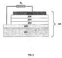
- Fig. 3 is a schematic showing the layers of one embodiment of a photovoltaic (PV) device.
- PV photovoltaic
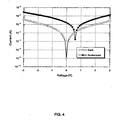
- Fig. 4 is a graph of the current versus voltage for the PV device of Example 15.
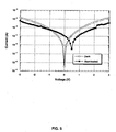
- Fig. 5 is a graph of the current versus voltage for the PV device of Example 16.
- One embodiment of the invention is a film comprising conducting polymer applied from a dispersion containing particles having a particle size of less than 450 nm, wherein the conducting polymer comprises substituted or unsubstituted, uncharged or charged polymerized units of thieno[3,4-b]thiophene, and wherein the film has a conductivity between 10 -1 to 10 -6 S/cm.
- the film is particularly useful as a hole injection layer, a hole transport layer or a combined hole injection and hole transport layer.
- the film is particularly useful in an optoelectronic device that is capable of the interconversion of light and electricity.
- dispersion is used herein to describe a system consisting of a disperse phase in a medium. It can be a dispersion, a solution, a colloid, an emulsion or the like.
- dispersion is used herein to describe the material used to form the film comprising the conducting polymer. It is understood that the material used to form the film may be a dispersion, a solution, a colloidal, an emulsion, or the like.
- film used herein, shall possess a broad definition encompassing any coating or deposit of the films of the present invention regardless of thickness, shape or structure. In certain embodiments, the thickness is at least 5 nm. Films can be formed by depositing a monomolecular layer of the composition. Several layers of the same or different compositions are also contemplated herein.
- thieno[3,4-b]thiophenes of this invention polymerize at high polymerization rates in the presence of polyanions, and form stable compositions preferably in solvent having the desired properties for optoelectronic applications.
- Water, or organic solvents such as, lower alcohols like methanol, ethanol, butanol or isopropanol as well as mixtures of water with said lower alcohols or with other water-miscible organic solvents like acetone are suitable as solvents for the compositions.
- the preferred solvents are water, or a water/alcohol mixture.
- aqueous medium will be used herein to refer to the solvent when it includes water or a mixture of water and one or more organic solvents used in the dispersions.
- the average particle diameter of the particles of the dispersions is less than 450 nm, preferably less than 200 nm.
- the present invention relates to dispersions of polymers in the presence of polyanions, wherein the polymers comprise structural units corresponding to the following formula (I): where R is hydrogen, substituted or unsubstituted (C 1 -C 18 )-alkyl, preferably (C 1 -C 10 )-alkyl, in particular (C 1 -C 6 )-alkyl, for example, t-butyl, (C 3 -C 7 )-cycloalkyl, (C 1 -C 18 )-alkyloxy, preferably (C 1 -C 10 )-alkyloxy, or (C 2 -C 18 )-alkyloxy ester, phenyl and substituted phenyl, and SF 5 .
- R is hydrogen, substituted or unsubstituted (C 1 -C 18 )-alkyl, preferably (C 1 -C 10 )-alkyl, in particular (C 1 -C 6 )-alkyl, for
- Suitable conductive polymers which may be used in accordance with the present invention include undoped or doped, soluble or insoluble thieno[3,4-b]thiophene based polymers comprising units of the formula (I), such as, the polymer shown in formula (II) where n represents an integer from 3 to 100 and R is hydrogen, substituted or unsubstituted (C 1 -C 18 )-alkyl, preferably (C 1 -C 10 )-alkyl, in particular (C 1 -C 6 )-alkyl, for example, t -butyl, (C 3 -C 7 )-cycloalkyl, (C 1 -C 18 )-alkyloxy, preferably (C 1 -C 10 )-alkyloxy, or (C 2 -C 18 )-alkyloxy ester, phenyl and substituted phenyl, and SF 5 .
- C 1 -C 18 )-alkyl preferably (C 1
- poly(thieno[3,4-b]thiophene) will be used to refer to homopolymers or copolymers comprising structural units corresponding to formula (I).
- the polyanions are anions of polymeric carboxylic acids, such as polyacrylic acids, polymethacrylic acids or polymaleic acids, and polymeric sulfonic acids, such as polystyrene sulfonic acids and polyvinyl sulfonic acids.
- polymeric carboxylic acids such as polyacrylic acids, polymethacrylic acids or polymaleic acids
- polymeric sulfonic acids such as polystyrene sulfonic acids and polyvinyl sulfonic acids.
- These polycarboxylic and polysulfonic acids may also be copolymers of vinyl carboxylic and vinyl sulfonic acids with other polymerizable monomers, such as acrylates and styrene.
- the molecular weight of the polyacids supplying the polyanions is preferably in the range form 1,000 to 1,500,000, more preferably in the range from 2,000 to 300,000, most preferably from 20,000 to 260,000.
- the polyanions can also be supplied by alkali salts of the polyacids.
- the polyacids or their alkali salts are commercially available, for example polystyrene sulfonic acids and polyacrylic acids, or may be produced by known methods.
- the dispersions comprising conducting polymer in the presence of polyanions according to the invention are obtained by oxidative polymerization of units corresponding to formula (I), with oxidizing agents typically used for the oxidative polymerization of pyrrole and/or with oxygen or air in the presence of the polyacids, preferably in aqueous medium, at temperatures from 4 °C to 50 °C, preferably from 8 °C to 22 °C, more preferably from 8 °C to 18 °C.
- the monomers corresponding to formula (I), polyanion(s) and oxidizing agent(s), and other optional components are dissolved or dispersed in an organic solvent, or preferably, in an aqueous medium and the resulting reaction mixture is stirred at the desired polymerization temperature.
- air or oxygen is used as the oxidizing agent, air or oxygen is introduced into the reaction mixture containing the monomers of formula (I), polyacid and, optionally, catalytic quantities of metal salts or other components during the whole polymerization period.
- the reaction mixture may be mixed before and/or during the polymerization.
- Mixing can be accomplished by several means including mechanical means.
- Preferred mechanical mixing is high shear mixing.
- shear mixing from 5000 rpm to 24,000 rpm is preferred.
- the polymerization can be carried out from 10 minutes to 24 hours, preferably from 20 minutes to 4 hours.
- the time for polymerization of the reaction mixture will vary with the composition of the reaction mixture, the temperature and the rate of mixing.
- the stability of the obtained dispersions may be improved by the addition of dispersing agents like sodium dodecyl sulphonate during or after polymerization.
- Suitable oxidizing agents are any of the oxidizing agents suitable for the oxidative polymerization of pyrrole which are described, for example, in J. Am. Soc. 85, 454 (1963).
- inexpensive and easy-to-handle oxidizing agents for example iron(III) salts, such as FeCl 3 , Fe(ClO 4 ) 3 , Fe 2 (SO 4 ) 3 , and the iron(III) salts of organic acids and inorganic acids containing organic residues, as well as H 2 O 2 , K 2 Cr 2 O 7 , alkali or ammonium persulfates, alkali perborates, potassium permanganate and copper salts, such as copper tetrafluoroborate.
- air and oxygen optionally in the presence of catalytic quantities of metal ions, such as iron, cobalt, nickel, molybdenum and vanadium ions, may advantageously be used as oxidizing agents.
- iron(III) salts of inorganic acids containing organic residues are the iron(III) salts of sulfuric acid semiesters of C 1-20 alkanols, for example, the Fe(III) salt of lauryl sulfate.
- iron(III) salts of organic acids are: the Fe(III) salts of C 1-30 alkyl sulfonic acids, such as methane or dodecane sulfonic acid; aliphatic C 1-20 carboxylic acids, such as 2-ethylhexyl carboxylic acid; aliphatic perfluorocarboxylic acids, such as trifluoroacetic acid and perfluorooctanoic acid; aliphatic dicarboxylic acids, such as oxalic acid and aromatic, optionally C 1-20 -alkyl-substituted sulfonic acids, such as benzenesulfonic acid, p-toluenesulfonic acid and dodecyl benzenesulfonic acid.
- C 1-30 alkyl sulfonic acids such as methane or dodecane sulfonic acid
- aliphatic C 1-20 carboxylic acids such as 2-ethylhexyl carb
- the polyanion to be used in accordance with the invention are added in such a quantity that, for every mol monomer corresponding to formula (I), there are 0.01 to 50 and preferably 0.1 to 30 mol anion groups of the polyanion.
- the monomers corresponding to formula (I) and the polyanion(s) are dissolved in such a quantity of solvent that stable poly(thieno[3,4-b]thiophene) dispersions are obtained having solid contents of 0.05 to 50% by weight and preferably 0.5 to 5% by weight.
- polymeric binder soluble or suspendable in water for example polyvinyl alcohol or polyvinyl acetate dispersions
- Ammonia or amines may be added to neutralize the dispersion after polymerization.
- solvents or cosolvents or additives, such as, surfactant may also be added to the dispersion.
- the polyanion(s) may be added to the reaction mixture prior to polymerization or may be added to the dispersion after polymerization. Dispersions may be obtained with less than 0.5 part by weight of the conducting polymer comprising units of formula (1) based on one part by weight of the polyanion(s).
- the dispersions used to form the films of this invention may comprise copolymers, comprising units of thieno[3,4-b]thiophene, and units of other monomers
- the monomers useful for forming copolymers include monomers known to form conducting polymers through oxidative polymerization, particularly other thiophene monomers. Examples of useful monomers used to form conducting polymers that can be added to the dispersions are disclosed in US 5,300,575, and US 4,959,430 incorporated herein by reference. Monomers used to form other known conducting polymers can be added to the reaction mixture used to form the dispersion prior to or during the polymerization. The total amount of monomers including the monomers of formula (I) added to the reaction mixture may be from 0.01 to 30 % by weight based on the total weight of the dispersion.
- Preferred dispersions of the conducting polymers contain less than 10 ppm of metal ions and/or less than 10 ppm of anions of inorganic acids. Particularly preferred are dispersions of the conducting polymers that contain less than 1 ppm of metal ions and/or less than 1 ppm of anions of inorganic acids.
- the particle size of the dispersions and the conductivity of films prepared from the dispersions can be adjusted by the composition and the process of preparation of the dispersions (for example, by adjusting the temperature, shear rate, and reaction times). This is important for optoelectronics, e.g. matrix display, particularly for passive matrix display, because crosstalk between neighboring pixels might occur due to low surface resistance of the films.
- the conductivity of the film can be optimized for the desired film thickness to yield a film that has a surface resistance necessary to suppress crosstalk.
- Fig. 1 is a graph showing the relationship between the measured drop cast film conductivity (measured from a drop cast film in an argon glove box using the four point probe method) and the polymerization reaction time for a reaction mixture at 9 °C used to form a dispersion and film in accordance with this invention.
- shorter reaction times would be required to obtain conductivities from 10 -1 to 10 -6 S/cm.
- polymerization temperatures less than 9°C longer reaction times would be required to obtain conductivities from 10 -1 to 10 -6 S/cm.
- the oxidative polymerizations of thieno[3,4-b]thiophene in the presence of polyanions can be carried out over a range of polymerization reaction times and temperatures.
- Preferred polymerization temperatures are from 7 °C, to about room temperature (22 °C). More preferred polymerization temperatures are from 8 °C to 18 °C.
- aqueous dispersions produced between 8 °C and 18 °C can be filtered through a 450 nm pore size filter and a 200 nm pore size filter.
- Any reference to a filter size herein means the pore size of the filter unless otherwise indicated.
- Filterability denotes a small particle size which is important in producing uniform (smooth) films made by spin casting of the aqueous dispersion of the doped conducting polymer.
- the dispersions of the conducting polymer are preferably filtered through a filter having a pore size less than or equal to 450 nm before the dispersions are used to form films, e.g. by coating onto substrates or other articles.
- the solutions or dispersions are filtered using filters with pore size less than or equal to 200 nm before the dispersions are used to form films.
- the films of this invention are typically applied to an article.
- the film application or fabrication methods include but are not limited to spin coating, doctor blade coating, ink jet printing, screen printing, thermal transfer printing, microcontact printing or digital printing. Thickness of the film can range from 2 nm to 1000 nm, preferably from 20 nm to 500 nm, or more preferably from 50 nm to 200 nm.
- the film may be heated at a temperature from 50 °C to 250 °C, preferably from 100 °C to 200 °C to remove the residual solvent, or other volatiles preferably in an inert atmosphere.
- the films of this invention are useful as a layer in an optoelectronic device.
- the film can be used to form the hole injection layer, hole transport layer or combined hole injection and hole transport layer (which may be referred to hereinafter as a "hole injection/transport layer") in an optoelectronic device.
- Examples of optoelectronic devices include light emitting diodes and photovoltaic devices.
- an LED 100 may be formed with a light emitting layer between two electrodes, in which the light emitting layer assumes a plurality of functions.
- the LED shown in Fig. 2 has a substrate 101, anode 102, hole injection layer 103, hole transport layer 104, light emitting layer 105, electron transport layer 106, electron injection layer 107, and cathode 108.
- the anode 102 and the cathode 108 is transparent. Since the device is sensitive to moisture/oxygen, the device is normally hermetically encapsulated for different applications.
- the LED shown in Figure 2 is one embodiment. Alternative embodiments may consist of fewer or more layers. If there are fewer individual layers, at least one of the remaining layers assumes a plurality of functions.
- Suitable materials for the substrate 101 include glass, metal foil, plastics such as poly(ethylene terephthalate), poly(ethylene naphthalate), polyester, polysulfone, polyimide, polycarbonate, polyacrylate, polyarylate, and the like.
- the substrate 101 will be transparent if the light is to be extracted from the device through the anode 102 in the embodiment shown in Fig. 2.
- a transparent cathode is used and a non-transparent substrate such as metal foil, can be used as the substrate 101.
- An encapsulation layer (not shown) is typically provided to seal the LED. If the encapsulation layer covers the layer from which light is emitted or extracted, it is preferably a transparent layer.
- Useful materials, such as glass and metal plates for the encapsulation layer are known in the art.
- Suitable anode materials for anode 102 include metal oxides such as tin oxide, ITO, zinc oxide, doped zinc oxide, a semitransparent thin film of metals such as Au, Pt, Cu, and Ag, etc., or conductive polymers such as polyaniline, poly(3,4-ethylenedioxythiophene) (PEDOT), US 5,766,515, and US 6,083,635, polythiophene, polypyrrole, and the like.
- metal oxides such as tin oxide, ITO, zinc oxide, doped zinc oxide, a semitransparent thin film of metals such as Au, Pt, Cu, and Ag, etc.
- conductive polymers such as polyaniline, poly(3,4-ethylenedioxythiophene) (PEDOT), US 5,766,515, and US 6,083,635, polythiophene, polypyrrole, and the like.
- the cathode 108 can be a material containing any metal or nonmetal capable of injecting electrons into the light emitting layer.
- the cathode normally has a lower work function than the anode material.
- Suitable materials for the cathode 108 are low work function metals such as aluminum, indium, calcium, barium, magnesium, silver, lithium, or the like, alloy such as Mg:Ag, and a combination of salts and metals, such as, LiF/Al, NaCl/Al, or LiF/Ca/Al, or the like.
- Semitransparent cathodes such as, very thin layers of the above mentioned metals in combination with ITO, can be used to fabricate OLEDs that emit light through the cathode.
- the cathode layer is usually applied by a physical vapor deposition process such as thermal deposition, plasma deposition, e-beam deposition, or sputtering.
- the light-emitting layer 105 may contain any organic electroluminescent material. Suitable materials for the light emitting layer include polymeric materials such as those described in U. S. Patent 5,247,190 (to Friend et al.), U. S. Patent 5,408,109 (to Heeger et al.), U.S.
- Patent 5,962,631 (to Woo et al.), which are incorporated herein by reference, poly(phenylene vinylene)s, such as, poly(2-methoxy, 5-(2'-ethyl-hexyloxy)-p-phenylene-vinylene) (MEH-PPV) and Covion's Super Yellow, polyfluorenes, such as, poly(9,9-dialkyl fluorene), poly(9,9-dialkyl fluorene)-co-2,1,3-benzothiadiazole, poly(9,9-diakylfluorene)-co-2,1,3-benzothiadiazole-co-thiophene, poly(para-phenylene), spiropolyfluorenes, and the like; small molecules, such as, 8-hydroxyquinoline aluminium (Alq 3 ), laser dyes, europium complex, and dendrimers, (J.
- Alq 3 8-hydroxyquinoline aluminium
- Phosphorescent compounds e. g., platinum octaethyl porphyrin (PtOEP), bis(2-(2'-benzothienyl)pyridinato-N,C 3' )acetylacetonate) Iridium (III), and tris(2-(4-tolyl)phenylpyridine) Iridium (III), which can utilize triplet excitons, and hence yield higher efficiency, can also be used for the light emitting layer 105.
- PtOEP platinum octaethyl porphyrin
- PtOEP bis(2-(2'-benzothienyl)pyridinato-N,C 3' )acetylacetonate) Iridium (III)
- tris(2-(4-tolyl)phenylpyridine) Iridium (III) which can utilize triplet excitons, and hence yield higher efficiency, can also be used for the light emitting layer 105.
- the light-emitting materials may be dispersed in a matrix of other material(s).
- the light-emitting layer generally has a thickness of 40 to 400 nm.
- the light emitting layer can be applied (onto the hole transport layer, hole injection layer or hole injection/transport layer) from solutions by any casting method, such as, spin-coating, ink-jet printing, screen printing, or digital printing.
- the light emitting layer can also be applied by a thermal transfer process. In the case of small molecules, the layer can be applied by thermal evaporation, or low pressure organic vapor phase deposition.
- the film of this invention can be used as either the hole injection layer (HIL) 103 or hole transport layer (HTL) 104 or can be used to replace the HIL 103 and HTL 104 as shown in Fig. 2 with a single hole injection/transport layer (not shown).
- the film of this invention when used as a hole injection/transport layer in one embodiment forms a clear interface between the anode layer 102 and the light emitting layer 105.
- the film of this invention is used as both the HIL and HTL in the LED; however, the film could be used in an LED as the HIL with a separate and/or different HTL therein, or the film could be used in an LED as the HTL with a separate and/or different HIL therein.
- an electron blocking layer can be inserted between the light emitting layer and the HIL or HTL (either or both of which may comprise films of this invention) to prevent electrons from reaching one or both of those layers.
- the film of this invention may have a more favorable work function compared with commonly used anode material ITO, the film may improve the injection of holes within the LED devices.
- the film of this invention may also have a higher conductivity compared with the light emitting polymer layer; therefore, it may also function as a hole transport layer.
- the film of this invention may act as a buffer layer, because the electric field in the film may be lower than in the light emitting layer, which will slow down the diffusion of ions such as ln 3+ .
- a photovoltaic (PV) device is a device that absorbs light and generates electricity.
- Fig. 3 shows the structure of one embodiment of a PV device, comprising substrate 201, anode 202, hole transporting layer 203, semiconductive hole transporting layer 204, semiconductive electron transporting layer 205, and cathode 206.
- Alternative embodiments of PV devices may have fewer or more layers than are shown in Figure 3.
- layers 204 and 205 can be substituted with a layer of interpenetrating network of the semiconductive hole transporting and electron transporting materials to increase the interfacial area where charge separation takes place.
- the substrate 201, the anode 202, and the cathode 206 can be the same materials as those described for the substrate 101, the anode 102, and the cathode 108 for the LED above, respectively.
- the hole transport layer 203 can comprise the film of this invention.
- the semiconductive hole transporting layer 204 may be made of small . molecules or polymers having hole transporting properties, such as MEH-PPV (G. Yu et al., J. of Electronic Materials 23, 925(1994)), phthalocyanine, and aryl amines.
- the semiconductive electron transporting layer 205 may be made of small molecules or polymers having electron transporting properties, such as CN-PPV (J. J. M. Halls et al. Nature 376, 498, 1995), N,N'-bis (2,5-di-tert-butylphenyl-3,4,9,10-perylenedicarboximide, and perylene-3,4,9,10-tetracarboxylic-4,4,9,10-dianhydride (PTCDA).
- the combination of semiconductive hole transporting material and electron transporting material should be selected based on their HOMO and LUMO energy level alignment, such that charge separation from excitons generated in one or both of the materials will be factilitated at the interface of the two materials.
- the light emitting diode or photovoltaic devices of the invention can be produced by the methods disclosed in the prior art, known to a person of skill in the art or as described in the examples below.
- Example 1 Poly(thieno[3,4-b]thiophene):poly(styrene sulfonic acid) (PTT) dispersion prepared at room temperature, film, and OLED (Comparative Example
- Dispersion 1 was not filterable with a 450 nm filter.
- a thin film was prepared by drop cast 0.5 mL of Dispersion 1 onto 1"x1" glass substrate. The film was dried in air and annealed at 160 °C for 30 minutes under nitrogen protection. The conductivity of the film was 1.60 ⁇ 10 -3 S/cm, measured by four point probe method in an argon filled glove box.
- a light emitting polymer solution of MEH-PPV, (ADS130RE from American Dye Source, Inc.) in toluene was prepared by dissolving 25.6 mg of MEH-PPV in 4.25 g of toluene. and then filtered with a 1000 nm PVDF (Polyvinylidene fluoride) filter.
- the solution is hereafter referred to as Solution A.
- An ITO coated glass substrate (2.5 ⁇ 2.5 ⁇ 0.7 cm, surface resistance ⁇ 12 ⁇ /square) was cleaned by ultrasonication sequentially in detergent, de-ionized water, methanol, isopropanol, and acetone; each for 5 to 10 minutes. The ITO substrate was allowed to dry between different cleaning solvents.
- the ITO substrate was treated with oxygen plasma in an SPI Prep II plasma etcher for about 10 minutes.
- the ITO substrate was spin coated with Dispersion 1 at 800 rpm for 2 minutes followed by 2000 rpm for 20 seconds on a Laurell Model WS-400-N6PP spinner to form the HIL. Since Dispersion 1 was not filterable, it was used without filtration.
- the thickness of the PTT layer was about 30 nm.
- the PTT coated ITO substrate was then annealed at 180°C for 15 minutes under nitrogen protection. Then a layer of about 70-nm-thick MEH-PPV was spin coated onto the HIL from Solution A at a spin rate of 1500 rpm.
- the sample was then transferred into the chamber of a vacuum evaporator, which was located inside an argon atmosphere glove box.
- a layer of 20 nm thick Ca was vacuum deposited at below 1 ⁇ 10 -7 Torr through a mask at a rate of 1.5 ⁇ 2.0 ⁇ /s, and another layer of 100 nm thick Ag was vacuum deposited on top of Ca as a protecting layer.
- the active area of the device was about 6.2 mm 2 .
- the LED device was then moved out of the glove box for testing in air at room temperature. Thicknesses were measured on a KLA Tencor P-15 Profiler. Current-voltage characteristics were measured on a Keithley 2400 SourceMeter. Electroluminescence (EL) spectrum of the device was measured using an Oriel InstaSpec IV CCD camera.
- the power of EL emission was measured using a Newport 2835-C multi-function optical meter in conjunction with a calibrated Si photodiode. Brightness was calculated using the EL forward output power and the EL spectrum of the device, assuming Lambertian distribution of the EL emission. The device showed very high leakage current and poor performance. The device reached 1 cd/m 2 at 4 V, with a maximum external quantum efficiency of only 0.16%. At a current density of 100 mA/cm 2 , the device showed a brightness of only 150 cd/m 2 . At a current density of 1000 mA/cm 2 , the brightness was only 2000 cd/m 2 .
- Dispersion 2 was filterable with a 450 nm filter. A thin film of Dispersion 2 was prepared and the conductivity of the film measured the same way as in Example 1. The conductivity was 8.94 ⁇ 10 -3 S/cm.
- An OLED device was fabricated and tested in the same way as Example 1 except that Dispersion 2 was used to spin coat the HIL. Dispersion 2 was filtered with a 450 nm PVDF filter before spin coating. The thickness of the PTT layer was about 30 nm. The device reached 1 cd/m 2 at 2.6 V, with a maximum external quantum efficiency of 0.55%. At a current density of 100 mA/cm 2 , the device showed a brightness of 850 cd/m 2 . At a current density of 1000 mA/cm 2 , the brightness was 7,900 cd/m 2 . The device showed relatively high leakage current.
- Dispersion 3 was filterable with a 450 nm filter. A thin film of Dispersion 3 was prepared and the conductivity of the film measured the same way as in Example 1. The conductivity was 1.82 ⁇ 10 -2 S/cm.
- An OLED device was fabricated and tested in the same way as Example 1 except that Dispersion 3 was used to spin coat the HIL. Dispersion 3 was filtered with a 450 nm PVDF filter before spin coating. The thickness of the PTT layer was about 30 nm. The device reached 1 cd/m 2 at 2.5 V, with a maximum external quantum efficiency of 0.55%. At a current density of 100 mA/cm 2 , the device showed a brightness of 1,000 cd/m 2 . At a current density of 1000 mA/cm 2 , the brightness was 8,700 cd/m 2 . The device also showed relatively high leakage current.
- Example 4 PTT dispersion prepared at 4 °C with high shear mixing, film and OLED
- Dispersion 4 was filterable with a 200 nm filter. A thin film of Dispersion 4 was prepared and the conductivity of the film measured the same way as in Example 1. The conductivity was 1.64 ⁇ 10 -6 S/cm.
- An OLED device was fabricated and tested in the same way as Example 1 except that Dispersion 4 was used to spin coat the HIL. Dispersion 4 was filtered with a 450 nm PVDF filter before spin coating. The thickness of the PTT layer was about 20 nm. The device reached 1 cd/m 2 at 2.5 V, with a maximum external quantum efficiency of 0.58%. At a current density of 100 mA/cm 2 , the device showed a brightness of 830 cd/m 2 . Due to the low conductivity of the PTT, the brightness of the device was limited. The maximum brightness of the device was 1,700 cvd/m 2 at a current density of 260 mA/cm 2 and 11 V.
- Dispersion 5 was filterable with a 200 nm filter.
- a thin film was prepared using Dispersion 5 and the conductivity of the film measured the same way as in Example 1. The conductivity was 2.16 ⁇ 10 -3 S/cm.
- An OLED device was fabricated and tested in the same way as Example 1 except that Dispersion 5 was used to spin coat the HIL. Dispersion 5 was filtered with a 450 nm PVDF filter before spin coating. The thickness of the PTT layer was about 30 nm. The device reached 1 cd/m 2 at 2.5 V, with a maximum external quantum efficiency of 0.77%. At a current density of 100 mA/cm 2 , the device showed a brightness of 1,300 cd/m 2 . At a current density of 1000 mA/cm 2 , the brightness was 9,280 cd/m 2 .
- Dispersion 6 was filterable with a 200 nm filter.
- a thin film of Dispersion 6 was prepared and the conductivity of the film measured the same way as in Example 1. The conductivity was 9.27 ⁇ 10 -4 S/cm.
- An OLED device was fabricated and tested in the same way as Example 1 except that Dispersion 6 was used to spin coat the HIL. Dispersion 6 was filtered with a 0.45 PVDF filter before spin coating. The thickness of the PTT layer was about 30 nm. The device reached 1 cd/m 2 at 2.3 V, with a maximum external quantum efficiency of 0.73%. At a current density of 100 mA/cm 2 , the device showed a brightness of 1,440 cd/m 2 . At a current density of 1000 mA/cm 2 , the device showed a brightness of 11,550 cd/m 2 .
- Example 7 PTT dispersion prepared at 9 °C with high shear mixing, film and OLED
- Dispersion 7 was filterable with a 200 nm filter.
- a thin film of Dispersion 7 was prepared and the conductivity of the film measured the same way as in Example 1. The conductivity was 3.24 ⁇ 10 -3 S/cm.
- An OLED device was fabricated and tested in the same way as Example 1 except that Dispersion 7 was used to spin coat the HIL. Dispersion 7 was filtered with a 450 nm PVDF filter before spin coating. The device reached 1 cd/m 2 at 2.2 V, with a maximum external quantum efficiency of 0.76%. At a current density of 100 mA/cm 2 , the device showed a brightness of 1,360 cd/m 2 . At a current density of 1000 mA/cm 2 , the brightness was 10,400 cd/m 2 .
- Example 8 PTT dispersion prepared at 9 °C with high shear mixing, film and OLED
- Dispersion 8 A dispersion was prepared following the same procedures as in Example 4, except that 3.5 g (24.96 mmol) of thieno[3,4-b]thiophene and 30.2 g of 70,000 Mw poly(styrenesulfonic acid) solution were used, 12.0 g of ferric sulfate hydrate was added, the reaction was carried out for 2.5 hour at 9 C, and the purification used 100 g of Amberlite IR-120 and 100 g of IRA-900 ion exchange resins. The dispersion is hereafter referred to as Dispersion 8. A thin film of Dispersion 8 was prepared and the conductivity of the film measured the same way as in Example 1. The conductivity was 2.32 ⁇ 10 -4 S/cm.
- Dispersion 8 was used to spin coat the HIL.
- Dispersion 8 was filtered with a 450 nm PVDF filter before spin coating.
- the thickness of the PTT layer was about 30 nm.
- the device reached 1 cd/m 2 at 2.1 V, with a maximum external quantum efficiency of 0.69%.
- the device At a current density of 100 mA/cm 2 , the device showed a brightness of 1,330 cd/m 2 .
- the brightness was 9,070 cd/m 2 .
- Example 9 PTT dispersion prepared at 9 °C with high shear, film and OLED
- Dispersion 9 was filterable with a 200 nm filter. A thin film of Dispersion 9 was prepared and the conductivity of the film measured the same way as in Example 1. The conductivity was 5.85 ⁇ 10 -7 S/cm.
- An OLED device was fabricated and tested the same way as in Example 1 except that Dispersion 9 was used to spin coat the HIL. Dispersion 9 was filtered with a 450 nm PVDF filter before spin coating. The thickness of the PTT layer was about 30 nm. The device showed very poor performance. Only very low current could be passed through the device. The device reached 1 cd/m 2 at 3.4 V, with a maximum external quantum efficiency of 0.59%. Due to the low conductivity of the PIT film, the emission of the device was very weak. The maximum brightness was 150 cd/m 2 at a current density of 51.5 mA/cm 2 and 11.9 V.
- Example 10 PTT dispersion prepared at 15 °C with high shear mixing, film and OLED
- Dispersion 10 was filterable with a 200 nm PVDF filter.
- a thin film of Dispersion 10 was prepared and the conductivity of the film measured the same way as in Example 1. The conductivity was 8.10 ⁇ 10 -4 S/cm.
- a light emitting polymer solution of MEH-PPV ADS130RE from American Dye Source, Inc.) in toluene was prepared by dissolving 22.5 mg of MEH-PPV in 3.15 g of toluene on a hot plate at 60 °C for 2 hr, and then filtered with a 1000 nm filter.
- the solution is hereafter referred to as Solution B.
- An OLED device was fabricated and tested the same way as in Example 1 except that Dispersion 10 was used to spin coat the HIL and Solution B was used to spin coat (at a spin rate of 2000 rpm) the 70-nm-thick MEH-PPV. Dispersion 10 was filtered with a 450 nm PVDF filter before spin coating. The thickness of the PTT layer was about 30 nm. The device reached 1 cd/m 2 at 2.2 V, with a maximum external quantum efficiency of 1.35%. At a current density of 100 mA/cm 2 , the device showed a brightness of 1,780 cd/m 2 . At a current density of 1000 mA/cm 2 , the brightness was 17,600 cd/m 2 .
- Dispersion 11 was filterable with a 200 nm filter.
- a thin film of Dispersion 11 was prepared and the conductivity of the film measured the same way as in Example 1. The conductivity was 1.73 ⁇ 10 -6 S/cm.
- An OLED device was fabricated and tested the same way as in Example 10 except that Dispersion 11 was used to spin coat the HIL. Dispersion 11 was filtered with a 450 nm PVDF filter before spin coating. The thickness of the PTT layer was about 30 nm. The device reached 1 cd/m 2 at 2.4 V, with a maximum external quantum efficiency of 1.15%. At a current density of 100 mA/cm 2 , the device showed a brightness of 1,590 cd/m 2 . The maximum brightness was 5,160 cd/m 2 at a current density of 520 mA/cm 2 and 9.5 V.
- a thin film of PEDOT was prepared using an electronic grade Baytron P Al 4083 PEDOT dipersion (from Bayer Corp.), and the conductivity of the film measured the same way as in Example 1. The conductivity was 1.83 ⁇ 10 -3 S/cm.
- An OLED device was fabricated and tested the same way as in Example 1 except that Baytron P Al 4083 PEDOT dispersion was used to spin coat the HIL at a spin rate of 2500 rpm.
- the PEDOT dispersion was filtered with a 450 nm PVDF filter before spin coating.
- the thickness of the PEDOT layer was about 40 nm.
- the device reached 1 cd/m 2 at 2.1 V, with a maximum external quantum efficiency of 0.63%.
- the device At a current density of 100 mA/cm 2 , the device showed a brightness of 1,260 cd/m 2 .
- At a current density of 1000 mA/cm 2 the device showed a brightness of 10,400 cd/m 2 .
- a thin film of PEDOT was prepared from electronic grade Baytron P CH8000 PEDOT dispersion (from Bayer Corp.), and the conductivity of the film measured the same way as in Example 1. The conductivity was 2.79 ⁇ 10 -5 S/cm.
- An OLED device was fabricated and tested the same way as in Example 1 except that electronic grade Baytron P CH8000 PEDOT dispersion was used to spin coat the HIL at a spin rate of 4000 rpm.
- the PEDOT dispersion was filtered with a 450 nm PVDF filter before spin coating.
- the thickness of the PEDOT layer was about 45 nm.
- the device reached 1 cd/m 2 at 2.2 V, with a maximum external quantum efficiency of 0.64%.
- the device showed a brightness of 1,040 cd/m 2 .
- the maximum brightness was 3,050 cd/m 2 at a current density of 460 mA/cm 2 and 8.3 V.
- Example 14 Triplet emitter and PTT based OLED
- a solution was prepared by dissolving 63.0 mg poly(N-vinylcarbazole) (from Aldrich), 27.0 mg 2-(4-biphenylyl)-5-(4-tert-butylphenyl)-1,3,4-oxadiazole (from Aldrich), and 4.8 mg of triplet emitter tris(2-(4-tolyl)phenylpyridine) iridium (III) (from American Dye Source, Inc.) in 4.0 g chlorobenzene. The solution was filtered with a 200 nm filter and hereafter referred to as Solution C.
- An OLED device was fabricated and tested the same way as in Example 1, except that the HIL was fabricated by spin coating Dispersion 2 (after being filtered with a 450 nm PVDF hydrophilic filter) at 1500 rpm for 1 minute and then annealed at 200 °C for 5 minutes under nitrogen protection, and the light emitting layer (135 nm thick) was spin coated from Solution C at a spin rate of 1000 rpm.
- the device turn-on voltage was 13.0 V, with a maximum efficiency of 4.5%, and a maximum brightness of 28,400 cd/m 2 .
- Table 1 summarizes the conductivity, filterability and device, performance of Examples 1 to 13.
- Examples 1, 9, 12 and 13 are Comparative Examples.
- V on is the voltage at which the device reaches a brightness of 1 cd/m 2 .
- a lower V on is desirable because it implies a lower operation voltage and, consequently, a higher power efficiency.
- the external quantum efficiency (EQE) is the number of photons emitted per electron injected.
- the maximum EQE's of the devices are listed. High efficiency is desirable.
- the brightnesses of the devices at current densities of 100 and 1000 mA/cm 2 are also listed, a larger number implies a brighter and more efficient device.
- the rectification ratios R 5 at ⁇ 5 V are also listed.
- R 5 is the ratio of the device current at +5 V to the device current at -5 V. Because a device with lower leakage current is ideal, a large value of R 5 is desirable.
- Example 1 Comparative Example
- the dispersions of this invention are filterable by a 450 nm filter.
- the conductivity is too low ( ⁇ 1 ⁇ 10 -6 S/cm)
- the device performance is also poor, with higher operation voltage and lower maximum brightness because the device cannot support high current density due to the low conductivity of the PTT layer.
- It was also surprisingly found that several of the PTT based devices (Examples 5, 6, 7, 8,10, and 11) achieved better performance than PEDOT based devices (Examples 12 and 13).
- Example 14 is a dispersion, film and LED of this invention that was made using phosphorescent emitter, small molecule tris(2-(4-tolyl)phenylpyridine) iridium (III). Phosphorescent emitter based devices can utilize the triplet excitons, therefore, the device has a higher efficiency (4.5%). This example demonstrates that the PTT film can be used for phosphorescent emitter based OLEDs.
- Example 15 Photovoltaic device using PTT as the Hole Transporting Layer (HTL)
- a solution was prepared by dissolving 8.2 mg of N,N'-bis (3-methylphenyl)-N,N'-diphenylbenzidine (CAS# 65181-78-4, from Aldrich), 7.6 mg of N,N'-bis (2,5-di-tert-butylphenyl-3,4,9,10-perylenedicarboximide (CAS # 83054-80-2, from Aldrich), 7.2 mg PAE-2 (a poly(arylene ether) (US 5,658,994) and 7.2 mg of Ardel D100 polyarylate (PAL) in 1.53 g of chlorobenzene and filtered with a 0.2 ⁇ m filter.
- the solution is referred to as Solution D.
- ITO substrate was cleaned and treated with oxygen plasma as in Example 1.
- the ITO substrate was spin coated with Dispersion 2 at a spin rate of 1000 rpm and then annealed at about 160 °C for 15 minutes under nitrogen protection.
- Solution D was applied onto the PTT layer at a spin rate of 1000 rpm.
- the sample was masked, and a layer of 150-nm-thick Al was deposited via thermal vacuum evaporation at a pressure of 1.1 ⁇ 10 -7 Torr.
- the active area of the device was about 7 mm 2 .
- the finished device was connected to a Keithley 2400 SourceMeter (ITO side to the positive electrode and Al to the negative electrode), and the current-voltage curves of the device in the dark and under the illumination of a 150 W Xenon lamp were measured. An open circuit voltage of 0.6 V and a short circuit current of 15.8 ⁇ A were obtained. The current-voltage characteristics are shown in Fig. 4.
- a solution was prepared by dissolving 6.4 mg of N,N'-bis (3-methylphenyl)-N,N'-diphenylbenzidine, 6.9 mg of N,N'-bis(2,5-di-tert-butylphenyl)-3,4,9,10-perylenedicarboximide, 3.8 mg MEH-PPV, and 3.2 mg of Ardel D100 polyarylate in 1.56 g of chlorobenzene and filtered with a 0.2 ⁇ m filter.
- the solution is referred to as Solution E.
- An ITO substrate was cleaned and treated with oxygen plasma as in Example 1.
- the ITO substrate was spin coated with Dispersion 2 at a spin rate of 1000 rpm and then annealed at about 160 °C for 15 minutes under nitrogen protection. Then Solution E was applied onto the PTT layer at a spin rate of 1000 rpm. Finally, a layer of 150-nm-thick Al was deposited and the device tested the same way as in Example 15. An open circuit voltage of 0.4 V and a short circuit current of 11.0 ⁇ A were obtained. The current-voltage characteristics are shown in Fig. 5. A control device without PTT layer was fabricated side by side for comparison. Under the same illumination condition, the control device had an open circuit voltage of less than 0.1 V.
Landscapes
- Chemical & Material Sciences (AREA)
- Engineering & Computer Science (AREA)
- Medicinal Chemistry (AREA)
- Organic Chemistry (AREA)
- Manufacturing & Machinery (AREA)
- Polymers & Plastics (AREA)
- Health & Medical Sciences (AREA)
- Chemical Kinetics & Catalysis (AREA)
- Materials Engineering (AREA)
- Physics & Mathematics (AREA)
- Spectroscopy & Molecular Physics (AREA)
- Mechanical Engineering (AREA)
- Life Sciences & Earth Sciences (AREA)
- Geology (AREA)
- Structural Engineering (AREA)
- Electroluminescent Light Sources (AREA)
- Polyoxymethylene Polymers And Polymers With Carbon-To-Carbon Bonds (AREA)
- Compositions Of Macromolecular Compounds (AREA)
- Manufacture Of Macromolecular Shaped Articles (AREA)
- Laminated Bodies (AREA)
Applications Claiming Priority (2)
| Application Number | Priority Date | Filing Date | Title |
|---|---|---|---|
| US755426 | 1996-11-22 | ||
| US10/755,426 US7270871B2 (en) | 2004-01-12 | 2004-01-12 | Dispersions and films comprising conducting polymer for optoelectronic devices |
Publications (1)
| Publication Number | Publication Date |
|---|---|
| EP1559739A1 true EP1559739A1 (en) | 2005-08-03 |
Family
ID=34654300
Family Applications (1)
| Application Number | Title | Priority Date | Filing Date |
|---|---|---|---|
| EP20050000280 Withdrawn EP1559739A1 (en) | 2004-01-12 | 2005-01-07 | Dispersions and films comprising conducting polymer for optoelectronic devices |
Country Status (8)
| Country | Link |
|---|---|
| US (2) | US7270871B2 (cg-RX-API-DMAC7.html) |
| EP (1) | EP1559739A1 (cg-RX-API-DMAC7.html) |
| JP (1) | JP4122338B2 (cg-RX-API-DMAC7.html) |
| KR (1) | KR100718035B1 (cg-RX-API-DMAC7.html) |
| CN (2) | CN101230128B (cg-RX-API-DMAC7.html) |
| MY (1) | MY139263A (cg-RX-API-DMAC7.html) |
| SG (1) | SG113559A1 (cg-RX-API-DMAC7.html) |
| TW (1) | TWI262940B (cg-RX-API-DMAC7.html) |
Cited By (9)
| Publication number | Priority date | Publication date | Assignee | Title |
|---|---|---|---|---|
| EP1652850A1 (en) * | 2004-10-04 | 2006-05-03 | Air Products And Chemicals, Inc. | Substituted thienothiophene monomers and conducting polymers |
| EP1647566A3 (en) * | 2004-10-13 | 2007-01-24 | Air Products And Chemicals, Inc. | Aqueous dispersions of polythienothiophenes with fluorinated ion exchange polymers as dopants |
| US7432340B2 (en) | 2002-07-11 | 2008-10-07 | Air Products And Chemicals, Inc. | Fluorinated alkyl substituted-thieno[3,4-]thiophene monomers and polymers therefrom |
| EP2014664A2 (en) | 2007-07-13 | 2009-01-14 | Air Products and Chemicals, Inc. | Heterocyclic fused selenophene monomers |
| EP1810986A3 (de) * | 2006-01-20 | 2009-07-08 | H.C. Starck GmbH | Polythiophenformulierungen zur Verbesserung von organischen Leuchtdioden |
| US7572879B2 (en) | 2002-07-11 | 2009-08-11 | Air Products And Chemicals, Inc. | Fluorinated alkyl substituted-thieno[3,4-b]thiophene monomers and polymers therefrom |
| US7850871B2 (en) | 2004-10-13 | 2010-12-14 | Air Products And Chemicals, Inc. | Resistivity stable electrically conductive films formed from polythiophenes |
| US8148548B2 (en) | 2007-07-13 | 2012-04-03 | Konarka Technologies, Inc. | Heterocyclic fused selenophene monomers |
| US20120119157A1 (en) * | 2009-07-24 | 2012-05-17 | Kuraray Co., Ltd. | Thiophene derivative, method for producing same, and polymer of thiophene derivative |
Families Citing this family (34)
| Publication number | Priority date | Publication date | Assignee | Title |
|---|---|---|---|---|
| US7687582B1 (en) * | 2001-08-31 | 2010-03-30 | Tda Research, Inc. | Methods of production, purification, and processing of poly(heteroaromatic) block copolymers with improved solubility or dispersability |
| WO2005103109A1 (en) * | 2004-04-20 | 2005-11-03 | Winther-Jensen Bjoern | Base-inhibited oxidative polymerization of thiophenes and anilines with iron (iii) salts |
| US7141924B2 (en) * | 2004-05-07 | 2006-11-28 | Au Optronics Corporation | Multi-layer cathode in organic light-emitting devices |
| WO2006084088A1 (en) * | 2005-01-31 | 2006-08-10 | University Of Connecticut | Conjugated polymer fiber, preparation and use thereof |
| US7268363B2 (en) * | 2005-02-15 | 2007-09-11 | Eastman Kodak Company | Photosensitive organic semiconductor compositions |
| WO2007008978A2 (en) * | 2005-07-11 | 2007-01-18 | University Of Connecticut | Electrochromic devices utilizing very low band gap conjugated polymers: preparation and use |
| US7737247B2 (en) * | 2005-07-11 | 2010-06-15 | The University Of Connecticut | Polymers of thieno[3,4-b]furan, method of making, and use thereof |
| JP2007103557A (ja) * | 2005-10-03 | 2007-04-19 | Shin Etsu Polymer Co Ltd | 固体電解質、電解コンデンサ及びにその製造方法 |
| US20070085061A1 (en) * | 2005-10-14 | 2007-04-19 | Elder Delwin L | Conductivity enhancement of conductive polymers by solvent exposure |
| TWI460741B (zh) * | 2006-02-09 | 2014-11-11 | Shinetsu Polymer Co | 導電性高分子溶液、導電性塗膜、電容器,以及電容器之製造方法 |
| JP5614933B2 (ja) | 2006-02-16 | 2014-10-29 | ユニバーシティ オブ コネチカット | 前駆体ポリマからの導電性ポリマ、その作製方法およびその使用 |
| US7563860B2 (en) * | 2006-04-06 | 2009-07-21 | Xerox Corporation | Semiconductors and electronic devices generated therefrom |
| JP4904903B2 (ja) * | 2006-04-20 | 2012-03-28 | 大日本印刷株式会社 | 有機エレクトロルミネッセンス素子の製造方法 |
| US8183319B2 (en) * | 2007-10-31 | 2012-05-22 | Air Products And Chemicals, Inc. | Film forming additive formulations of conductive polymers |
| US8168671B2 (en) * | 2008-06-26 | 2012-05-01 | The University Of Connecticut | Synthesis of thieno[3,4-b]thiophene, thieno[3,4-b]furan, related compounds and their derivatives and use thereof |
| JP2010114066A (ja) * | 2008-10-06 | 2010-05-20 | Fujifilm Corp | 有機導電性高分子塗布液、有機導電性高分子膜、導電体、及び抵抗膜式タッチパネル |
| KR101750301B1 (ko) | 2009-05-29 | 2017-06-23 | 가부시키가이샤 한도오따이 에네루기 켄큐쇼 | 발광 소자, 발광 장치, 전자기기 및 조명 장치 |
| US8329505B2 (en) * | 2010-01-29 | 2012-12-11 | Lock Haven University Of Pennsylvania | Method for deposition of cathodes for polymer optoelectronic devices |
| KR20120055386A (ko) * | 2010-11-23 | 2012-05-31 | 삼성전자주식회사 | 태양전지 및 그 제조방법 |
| DE102011016567B4 (de) * | 2011-04-08 | 2023-05-11 | OSRAM Opto Semiconductors Gesellschaft mit beschränkter Haftung | Verfahren zum Herstellen eines optoelektronischen Bauelements und derart hergestelltes Bauelement |
| JP5652314B2 (ja) * | 2011-04-28 | 2015-01-14 | コニカミノルタ株式会社 | 有機光電変換素子およびその製造方法 |
| WO2013112777A1 (en) * | 2012-01-25 | 2013-08-01 | Kemet Electronics Corporation | Polymerization method for preparing conductive polymer |
| US9685567B2 (en) * | 2012-07-20 | 2017-06-20 | Nutech Ventures | Nanocomposite photodetector |
| US10651409B2 (en) | 2012-07-20 | 2020-05-12 | Nutech Ventures | Narrowband nanocomposite photodetector |
| CN103936969B (zh) * | 2013-01-23 | 2016-04-13 | 海洋王照明科技股份有限公司 | 含噻吩并噻吩-二苯并噻吩苯并二噻吩的共轭聚合物及其制备方法与应用 |
| GB201317966D0 (en) * | 2013-10-10 | 2013-11-27 | Univ Manchester | Nanoparticles |
| WO2015089001A1 (en) * | 2013-12-11 | 2015-06-18 | Rhodia Operations | Polymer films, gels, and foams containing electrically conductive patterns, and electronic devices containing such films, gels, and foams |
| CN109155365B (zh) | 2016-05-19 | 2022-12-13 | 凯米特电子公司 | 用于固体电解电容器中的导电聚合物的聚阴离子共聚物 |
| US11177076B2 (en) | 2017-10-18 | 2021-11-16 | Kemet Electronics Corporation | Conductive polymer capacitor for improved reliability |
| US10658121B2 (en) | 2017-10-18 | 2020-05-19 | Kemet Electronics Corporation | Process for forming a solid electrolytic capacitor |
| US10943742B2 (en) | 2017-10-18 | 2021-03-09 | Kemet Electronics Corporation | Conductive polymer dispersion for improved reliability |
| SG11202107556SA (en) * | 2019-01-16 | 2021-08-30 | Univ Michigan Regents | Photodetectors with semiconductor active layers for under-display fingerprint and gesture sensors |
| JP7586668B2 (ja) * | 2020-08-21 | 2024-11-19 | 信越ポリマー株式会社 | 導電性高分子分散液の製造方法、及び導電性フィルムの製造方法 |
| DE112021004836T5 (de) | 2020-09-17 | 2023-07-13 | Kemet Electronics Corporation | Leitfähige polymerdispersion für verbesserte zuverlässigkeit |
Citations (5)
| Publication number | Priority date | Publication date | Assignee | Title |
|---|---|---|---|---|
| US4639328A (en) * | 1983-11-25 | 1987-01-27 | Merck Patent Gesellschaft Mit Beschrankter Haftung | Thienothiophene derivatives |
| JPH0338588A (ja) * | 1989-07-03 | 1991-02-19 | Daiso Co Ltd | チオフェン誘導体とこれを成分とする錯体及びその製造法 |
| EP1275651A2 (en) * | 2001-07-09 | 2003-01-15 | MERCK PATENT GmbH | Thienothiophene derivatives |
| EP1300430A1 (en) * | 2001-09-29 | 2003-04-09 | MERCK PATENT GmbH | Mono-, oligo- and polymers of benzo[b]thiophene and 2,2'-bisbenzo[b]thiophene and their use as charge transport materials |
| US20040074779A1 (en) * | 2002-07-11 | 2004-04-22 | Sotzing Gregory Allen | Polymeric compositions comprising thieno[3,4-b]thiophene, method of making, and use thereof |
Family Cites Families (16)
| Publication number | Priority date | Publication date | Assignee | Title |
|---|---|---|---|---|
| DE3422316C2 (de) * | 1984-06-15 | 1986-11-20 | Zipperling Kessler & Co (Gmbh & Co), 2070 Ahrensburg | Verfahren zur Herstellung von verformbaren Polymerblends aus elektrisch leitfähigen organischen Polymeren und/oder organischen Leitern, Vorrichtung zur Durchführung des Verfahrens sowie Verwendung der Polymerblends |
| DE3729566A1 (de) * | 1987-09-04 | 1989-03-16 | Zipperling Kessler & Co | Intrinsisch leitfaehiges polymer in form eines dispergierbaren feststoffes, dessen herstellung und dessen verwendung |
| US5066731A (en) * | 1987-10-26 | 1991-11-19 | Hoechst Aktiengesellschaft | Process for modifying electroconductive polymers using ion exchange |
| DE3804521A1 (de) * | 1988-02-13 | 1989-08-24 | Hoechst Ag | Elektrisch leitende beschichtungsmasse, verfahren zu ihrer herstellung und ihre verwendung |
| DE3843412A1 (de) * | 1988-04-22 | 1990-06-28 | Bayer Ag | Neue polythiophene, verfahren zu ihrer herstellung und ihre verwendung |
| DE3814730A1 (de) * | 1988-04-30 | 1989-11-09 | Bayer Ag | Feststoff-elektrolyte und diese enthaltende elektrolyt-kondensatoren |
| US5498761A (en) * | 1988-10-11 | 1996-03-12 | Wessling; Bernhard | Process for producing thin layers of conductive polymers |
| EP0440957B1 (de) * | 1990-02-08 | 1996-03-27 | Bayer Ag | Neue Polythiophen-Dispersionen, ihre Herstellung und ihre Verwendung |
| DE69319200T2 (de) * | 1992-10-14 | 1999-01-28 | Agfa-Gevaert N.V., Mortsel | Antistatische Beschichtungszusammensetzung |
| JP3534445B2 (ja) * | 1993-09-09 | 2004-06-07 | 隆一 山本 | ポリチオフェンを用いたel素子 |
| DE19507413A1 (de) * | 1994-05-06 | 1995-11-09 | Bayer Ag | Leitfähige Beschichtungen |
| DE19524132A1 (de) * | 1995-07-03 | 1997-01-09 | Bayer Ag | Kratzfeste leitfähige Beschichtungen |
| DE19810932A1 (de) * | 1998-03-13 | 1999-09-16 | Bayer Ag | Elektrochrome Anordnung auf Basis von Poly-(3,4-ethylendioxy-thiophen)-Derivaten |
| DE19841803A1 (de) * | 1998-09-12 | 2000-03-16 | Bayer Ag | Hilfsschichten für elektrolumineszierende Anordnungen |
| US7071289B2 (en) * | 2002-07-11 | 2006-07-04 | The University Of Connecticut | Polymers comprising thieno [3,4-b]thiophene and methods of making and using the same |
| US7105237B2 (en) * | 2003-10-01 | 2006-09-12 | The University Of Connecticut | Substituted thieno[3,4-B]thiophene polymers, method of making, and use thereof |
-
2004
- 2004-01-12 US US10/755,426 patent/US7270871B2/en not_active Expired - Lifetime
-
2005
- 2005-01-06 MY MYPI20050054A patent/MY139263A/en unknown
- 2005-01-06 SG SG200500136A patent/SG113559A1/en unknown
- 2005-01-07 EP EP20050000280 patent/EP1559739A1/en not_active Withdrawn
- 2005-01-12 CN CN200710159891.5A patent/CN101230128B/zh not_active Expired - Lifetime
- 2005-01-12 JP JP2005005398A patent/JP4122338B2/ja not_active Expired - Lifetime
- 2005-01-12 CN CNB2005100090846A patent/CN100471899C/zh not_active Expired - Lifetime
- 2005-01-12 TW TW94100871A patent/TWI262940B/zh not_active IP Right Cessation
- 2005-01-12 KR KR1020050002860A patent/KR100718035B1/ko not_active Expired - Lifetime
-
2007
- 2007-09-14 US US11/855,283 patent/US8920678B2/en active Active
Patent Citations (5)
| Publication number | Priority date | Publication date | Assignee | Title |
|---|---|---|---|---|
| US4639328A (en) * | 1983-11-25 | 1987-01-27 | Merck Patent Gesellschaft Mit Beschrankter Haftung | Thienothiophene derivatives |
| JPH0338588A (ja) * | 1989-07-03 | 1991-02-19 | Daiso Co Ltd | チオフェン誘導体とこれを成分とする錯体及びその製造法 |
| EP1275651A2 (en) * | 2001-07-09 | 2003-01-15 | MERCK PATENT GmbH | Thienothiophene derivatives |
| EP1300430A1 (en) * | 2001-09-29 | 2003-04-09 | MERCK PATENT GmbH | Mono-, oligo- and polymers of benzo[b]thiophene and 2,2'-bisbenzo[b]thiophene and their use as charge transport materials |
| US20040074779A1 (en) * | 2002-07-11 | 2004-04-22 | Sotzing Gregory Allen | Polymeric compositions comprising thieno[3,4-b]thiophene, method of making, and use thereof |
Non-Patent Citations (5)
| Title |
|---|
| LEE K. AND SOTZING G. A., MACROMOLECULES, vol. x, no. 34, 2001, pages 5746 - 5747, XP002329969 * |
| PATENT ABSTRACTS OF JAPAN vol. 015, no. 173 (C - 0828) 2 May 1991 (1991-05-02) * |
| POMERANTZ M. AND XIAOMIN G.: "Poly(2-decylthieno[3,4-b]thiophene). A New Soluble Low-Bandgap Conducting Polymer", SYNTHETIC METALS, vol. 84, 1997, pages 243 - 244, XP002329967 * |
| POMERANTZ M. ET AL: "Poly(2-decylthieno[3,4-b]thiophene-4,6-diyl). A New Low Band Gap Conducting Poymer", MACROMOLECULES, vol. 34, 2001, pages 1817 - 1822, XP002329966 * |
| SOTZING G. AND LEE K.: "Poly(thieno[3,4-b]thiophene): A p- and n-Dopable Polythiophene Exhibiting High Optical Transparency in the Semiconducting State", MACROMOLECULES, vol. 35, 2002, pages 7281 - 7286, XP002329968 * |
Cited By (13)
| Publication number | Priority date | Publication date | Assignee | Title |
|---|---|---|---|---|
| US7572879B2 (en) | 2002-07-11 | 2009-08-11 | Air Products And Chemicals, Inc. | Fluorinated alkyl substituted-thieno[3,4-b]thiophene monomers and polymers therefrom |
| US7432340B2 (en) | 2002-07-11 | 2008-10-07 | Air Products And Chemicals, Inc. | Fluorinated alkyl substituted-thieno[3,4-]thiophene monomers and polymers therefrom |
| US7118692B2 (en) | 2004-10-04 | 2006-10-10 | Air Products And Chemicals, Inc. | Substituted thienothiophene monomers and conducting polymers |
| EP1652850A1 (en) * | 2004-10-04 | 2006-05-03 | Air Products And Chemicals, Inc. | Substituted thienothiophene monomers and conducting polymers |
| EP1647566A3 (en) * | 2004-10-13 | 2007-01-24 | Air Products And Chemicals, Inc. | Aqueous dispersions of polythienothiophenes with fluorinated ion exchange polymers as dopants |
| US7850871B2 (en) | 2004-10-13 | 2010-12-14 | Air Products And Chemicals, Inc. | Resistivity stable electrically conductive films formed from polythiophenes |
| EP1810986A3 (de) * | 2006-01-20 | 2009-07-08 | H.C. Starck GmbH | Polythiophenformulierungen zur Verbesserung von organischen Leuchtdioden |
| US8252889B2 (en) | 2006-01-20 | 2012-08-28 | Heraeus Precious Metals Gmbh & Co. Kg | Polythiophene formulations for improving organic light emitting diodes |
| EP2014664A2 (en) | 2007-07-13 | 2009-01-14 | Air Products and Chemicals, Inc. | Heterocyclic fused selenophene monomers |
| EP2014664A3 (en) * | 2007-07-13 | 2011-10-05 | Konarka Technologies, Inc. | Heterocyclic fused selenophene monomers |
| US8148548B2 (en) | 2007-07-13 | 2012-04-03 | Konarka Technologies, Inc. | Heterocyclic fused selenophene monomers |
| US20120119157A1 (en) * | 2009-07-24 | 2012-05-17 | Kuraray Co., Ltd. | Thiophene derivative, method for producing same, and polymer of thiophene derivative |
| US9039936B2 (en) * | 2009-07-24 | 2015-05-26 | Tokyo Institute Of Technology | Thiophene derivative, method for producing same, and polymer of thiophene derivative |
Also Published As
| Publication number | Publication date |
|---|---|
| CN1651490A (zh) | 2005-08-10 |
| TWI262940B (en) | 2006-10-01 |
| JP2005206839A (ja) | 2005-08-04 |
| JP4122338B2 (ja) | 2008-07-23 |
| US20080023674A1 (en) | 2008-01-31 |
| US8920678B2 (en) | 2014-12-30 |
| KR100718035B1 (ko) | 2007-05-16 |
| TW200525011A (en) | 2005-08-01 |
| CN100471899C (zh) | 2009-03-25 |
| CN101230128B (zh) | 2014-11-05 |
| CN101230128A (zh) | 2008-07-30 |
| US20050151122A1 (en) | 2005-07-14 |
| SG113559A1 (en) | 2005-08-29 |
| US7270871B2 (en) | 2007-09-18 |
| KR20050074323A (ko) | 2005-07-18 |
| MY139263A (en) | 2009-09-30 |
Similar Documents
| Publication | Publication Date | Title |
|---|---|---|
| US8920678B2 (en) | Dispersions and films comprising conducting polymer for optoelectronic devices | |
| CN102174246B (zh) | 带有氟化离子交换聚合物作为掺杂物的聚噻吩并噻吩的水分散体 | |
| US8674047B2 (en) | Doping conjugated polymers and devices | |
| CN101679714B (zh) | 空穴注入层/传输层组合物及装置 | |
| EP2350216B1 (en) | Charge injection and transport layers | |
| EP1537612B1 (en) | Method of forming an optical device | |
| KR101422454B1 (ko) | 유기 광전 반도체 장치 및 그 제조방법 | |
| US7033646B2 (en) | High resistance polyaniline blend for use in high efficiency pixellated polymer electroluminescent devices | |
| JP2005248163A (ja) | 第1導電性共役ポリマーと第2導電性共役ポリマーとを含む水性ブレンド及びフィルム | |
| KR20060025538A (ko) | 고분자 | |
| Bolink et al. | Optimization of Polymer Blue‐Light‐Emitting Devices by Introducing a Hole‐Injection Layer Doped with the Molecular Nanomagnet [Mn12O12 (H2O) 4 (C6F5COO) 16] | |
| WO2012078517A1 (en) | Inks for solar cell inverted structures | |
| US20060011889A1 (en) | Semiconducting compositions comprising guest material and organic light emitting host material, methods for preparing such compositions, and devices made therewith | |
| Huang et al. | Materials and Interface Engineering in Organic Light-Emitting Diodes | |
| HK1240607A1 (en) | Doping conjugated polymers and devices | |
| HK1174934A (en) | Doping conjugated polymers and devices |
Legal Events
| Date | Code | Title | Description |
|---|---|---|---|
| PUAI | Public reference made under article 153(3) epc to a published international application that has entered the european phase |
Free format text: ORIGINAL CODE: 0009012 |
|
| AK | Designated contracting states |
Kind code of ref document: A1 Designated state(s): AT BE BG CH CY CZ DE DK EE ES FI FR GB GR HU IE IS IT LI LT LU MC NL PL PT RO SE SI SK TR |
|
| AX | Request for extension of the european patent |
Extension state: AL BA HR LV MK YU |
|
| 17P | Request for examination filed |
Effective date: 20050825 |
|
| AKX | Designation fees paid |
Designated state(s): AT BE BG CH CY CZ DE DK EE ES FI FR GB GR HU IE IS IT LI LT LU MC NL PL PT RO SE SI SK TR |
|
| STAA | Information on the status of an ep patent application or granted ep patent |
Free format text: STATUS: THE APPLICATION IS DEEMED TO BE WITHDRAWN |
|
| 18D | Application deemed to be withdrawn |
Effective date: 20110503 |