EP1558949B1 - Verfahren zur herstellung einer mechanisch haltbaren einlagigen beschichtung mit anti-reflex eigenschaften - Google Patents
Verfahren zur herstellung einer mechanisch haltbaren einlagigen beschichtung mit anti-reflex eigenschaften Download PDFInfo
- Publication number
- EP1558949B1 EP1558949B1 EP03772952A EP03772952A EP1558949B1 EP 1558949 B1 EP1558949 B1 EP 1558949B1 EP 03772952 A EP03772952 A EP 03772952A EP 03772952 A EP03772952 A EP 03772952A EP 1558949 B1 EP1558949 B1 EP 1558949B1
- Authority
- EP
- European Patent Office
- Prior art keywords
- nano
- particles
- process according
- acrylate
- meth
- Prior art date
- Legal status (The legal status is an assumption and is not a legal conclusion. Google has not performed a legal analysis and makes no representation as to the accuracy of the status listed.)
- Expired - Lifetime
Links
- 238000000034 method Methods 0.000 title claims abstract description 61
- 239000002356 single layer Substances 0.000 title claims abstract description 14
- 230000003667 anti-reflective effect Effects 0.000 title abstract description 27
- 238000000576 coating method Methods 0.000 title description 77
- 239000011248 coating agent Substances 0.000 title description 45
- 238000002360 preparation method Methods 0.000 title description 7
- 239000000203 mixture Substances 0.000 claims abstract description 103
- 239000000463 material Substances 0.000 claims abstract description 90
- 238000004132 cross linking Methods 0.000 claims abstract description 79
- 230000008569 process Effects 0.000 claims abstract description 50
- 239000002105 nanoparticle Substances 0.000 claims abstract description 47
- 239000000758 substrate Substances 0.000 claims abstract description 38
- 239000002904 solvent Substances 0.000 claims abstract description 30
- 229920002153 Hydroxypropyl cellulose Polymers 0.000 claims abstract description 10
- 239000001863 hydroxypropyl cellulose Substances 0.000 claims abstract description 10
- 235000010977 hydroxypropyl cellulose Nutrition 0.000 claims abstract description 10
- 230000001939 inductive effect Effects 0.000 claims abstract description 3
- OKKJLVBELUTLKV-UHFFFAOYSA-N Methanol Chemical class OC OKKJLVBELUTLKV-UHFFFAOYSA-N 0.000 claims description 30
- -1 diethyl acetate Chemical compound 0.000 claims description 30
- 239000002245 particle Substances 0.000 claims description 24
- 239000000178 monomer Substances 0.000 claims description 15
- XLYOFNOQVPJJNP-UHFFFAOYSA-N water Substances O XLYOFNOQVPJJNP-UHFFFAOYSA-N 0.000 claims description 11
- ZWEHNKRNPOVVGH-UHFFFAOYSA-N 2-Butanone Chemical class CCC(C)=O ZWEHNKRNPOVVGH-UHFFFAOYSA-N 0.000 claims description 9
- YMWUJEATGCHHMB-UHFFFAOYSA-N Dichloromethane Chemical compound ClCCl YMWUJEATGCHHMB-UHFFFAOYSA-N 0.000 claims description 9
- WYURNTSHIVDZCO-UHFFFAOYSA-N Tetrahydrofuran Chemical compound C1CCOC1 WYURNTSHIVDZCO-UHFFFAOYSA-N 0.000 claims description 8
- FDPIMTJIUBPUKL-UHFFFAOYSA-N pentan-3-one Chemical compound CCC(=O)CC FDPIMTJIUBPUKL-UHFFFAOYSA-N 0.000 claims description 8
- WEVYAHXRMPXWCK-UHFFFAOYSA-N Acetonitrile Chemical compound CC#N WEVYAHXRMPXWCK-UHFFFAOYSA-N 0.000 claims description 6
- HEDRZPFGACZZDS-UHFFFAOYSA-N Chloroform Chemical compound ClC(Cl)Cl HEDRZPFGACZZDS-UHFFFAOYSA-N 0.000 claims description 6
- LFQSCWFLJHTTHZ-UHFFFAOYSA-N Ethanol Chemical compound CCO LFQSCWFLJHTTHZ-UHFFFAOYSA-N 0.000 claims description 6
- XEKOWRVHYACXOJ-UHFFFAOYSA-N Ethyl acetate Chemical compound CCOC(C)=O XEKOWRVHYACXOJ-UHFFFAOYSA-N 0.000 claims description 6
- KFZMGEQAYNKOFK-UHFFFAOYSA-N Isopropanol Chemical class CC(C)O KFZMGEQAYNKOFK-UHFFFAOYSA-N 0.000 claims description 6
- ZMXDDKWLCZADIW-UHFFFAOYSA-N N,N-Dimethylformamide Chemical compound CN(C)C=O ZMXDDKWLCZADIW-UHFFFAOYSA-N 0.000 claims description 6
- YXFVVABEGXRONW-UHFFFAOYSA-N Toluene Chemical compound CC1=CC=CC=C1 YXFVVABEGXRONW-UHFFFAOYSA-N 0.000 claims description 6
- BDERNNFJNOPAEC-UHFFFAOYSA-N propan-1-ol Chemical class CCCO BDERNNFJNOPAEC-UHFFFAOYSA-N 0.000 claims description 6
- CSCPPACGZOOCGX-UHFFFAOYSA-N Acetone Chemical compound CC(C)=O CSCPPACGZOOCGX-UHFFFAOYSA-N 0.000 claims description 5
- 238000010438 heat treatment Methods 0.000 claims description 5
- 125000000962 organic group Chemical group 0.000 claims description 5
- QQZOPKMRPOGIEB-UHFFFAOYSA-N 2-Oxohexane Chemical class CCCCC(C)=O QQZOPKMRPOGIEB-UHFFFAOYSA-N 0.000 claims description 4
- ZPVFWPFBNIEHGJ-UHFFFAOYSA-N 2-octanone Chemical class CCCCCCC(C)=O ZPVFWPFBNIEHGJ-UHFFFAOYSA-N 0.000 claims description 4
- AMQJEAYHLZJPGS-UHFFFAOYSA-N N-Pentanol Chemical class CCCCCO AMQJEAYHLZJPGS-UHFFFAOYSA-N 0.000 claims description 4
- XUIMIQQOPSSXEZ-UHFFFAOYSA-N Silicon Chemical compound [Si] XUIMIQQOPSSXEZ-UHFFFAOYSA-N 0.000 claims description 4
- XLOMVQKBTHCTTD-UHFFFAOYSA-N Zinc monoxide Chemical compound [Zn]=O XLOMVQKBTHCTTD-UHFFFAOYSA-N 0.000 claims description 4
- JHIVVAPYMSGYDF-UHFFFAOYSA-N cyclohexanone Chemical compound O=C1CCCCC1 JHIVVAPYMSGYDF-UHFFFAOYSA-N 0.000 claims description 4
- BGTOWKSIORTVQH-UHFFFAOYSA-N cyclopentanone Chemical compound O=C1CCCC1 BGTOWKSIORTVQH-UHFFFAOYSA-N 0.000 claims description 4
- RLSSMJSEOOYNOY-UHFFFAOYSA-N m-cresol Chemical compound CC1=CC=CC(O)=C1 RLSSMJSEOOYNOY-UHFFFAOYSA-N 0.000 claims description 4
- XNLICIUVMPYHGG-UHFFFAOYSA-N pentan-2-one Chemical class CCCC(C)=O XNLICIUVMPYHGG-UHFFFAOYSA-N 0.000 claims description 4
- PGMYKACGEOXYJE-UHFFFAOYSA-N pentyl acetate Chemical compound CCCCCOC(C)=O PGMYKACGEOXYJE-UHFFFAOYSA-N 0.000 claims description 4
- YLQBMQCUIZJEEH-UHFFFAOYSA-N tetrahydrofuran Natural products C=1C=COC=1 YLQBMQCUIZJEEH-UHFFFAOYSA-N 0.000 claims description 4
- ISWSIDIOOBJBQZ-UHFFFAOYSA-N Phenol Chemical compound OC1=CC=CC=C1 ISWSIDIOOBJBQZ-UHFFFAOYSA-N 0.000 claims description 3
- TWNQGVIAIRXVLR-UHFFFAOYSA-N oxo(oxoalumanyloxy)alumane Chemical compound O=[Al]O[Al]=O TWNQGVIAIRXVLR-UHFFFAOYSA-N 0.000 claims description 3
- RVTZCBVAJQQJTK-UHFFFAOYSA-N oxygen(2-);zirconium(4+) Chemical compound [O-2].[O-2].[Zr+4] RVTZCBVAJQQJTK-UHFFFAOYSA-N 0.000 claims description 3
- 229910001928 zirconium oxide Inorganic materials 0.000 claims description 3
- DNIAPMSPPWPWGF-GSVOUGTGSA-N (R)-(-)-Propylene glycol Chemical class C[C@@H](O)CO DNIAPMSPPWPWGF-GSVOUGTGSA-N 0.000 claims description 2
- BYEAHWXPCBROCE-UHFFFAOYSA-N 1,1,1,3,3,3-hexafluoropropan-2-ol Chemical class FC(F)(F)C(O)C(F)(F)F BYEAHWXPCBROCE-UHFFFAOYSA-N 0.000 claims description 2
- CSUFEOXMCRPQBB-UHFFFAOYSA-N 1,1,2,2-tetrafluoropropan-1-ol Chemical compound CC(F)(F)C(O)(F)F CSUFEOXMCRPQBB-UHFFFAOYSA-N 0.000 claims description 2
- RYHBNJHYFVUHQT-UHFFFAOYSA-N 1,4-Dioxane Chemical compound C1COCCO1 RYHBNJHYFVUHQT-UHFFFAOYSA-N 0.000 claims description 2
- XNWFRZJHXBZDAG-UHFFFAOYSA-N 2-METHOXYETHANOL Chemical class COCCO XNWFRZJHXBZDAG-UHFFFAOYSA-N 0.000 claims description 2
- ISPYQTSUDJAMAB-UHFFFAOYSA-N 2-chlorophenol Chemical compound OC1=CC=CC=C1Cl ISPYQTSUDJAMAB-UHFFFAOYSA-N 0.000 claims description 2
- WXNZTHHGJRFXKQ-UHFFFAOYSA-N 4-chlorophenol Chemical class OC1=CC=C(Cl)C=C1 WXNZTHHGJRFXKQ-UHFFFAOYSA-N 0.000 claims description 2
- XDTMQSROBMDMFD-UHFFFAOYSA-N Cyclohexane Chemical compound C1CCCCC1 XDTMQSROBMDMFD-UHFFFAOYSA-N 0.000 claims description 2
- IAZDPXIOMUYVGZ-UHFFFAOYSA-N Dimethylsulphoxide Chemical compound CS(C)=O IAZDPXIOMUYVGZ-UHFFFAOYSA-N 0.000 claims description 2
- NTIZESTWPVYFNL-UHFFFAOYSA-N Methyl isobutyl ketone Chemical class CC(C)CC(C)=O NTIZESTWPVYFNL-UHFFFAOYSA-N 0.000 claims description 2
- UIHCLUNTQKBZGK-UHFFFAOYSA-N Methyl isobutyl ketone Chemical class CCC(C)C(C)=O UIHCLUNTQKBZGK-UHFFFAOYSA-N 0.000 claims description 2
- WRQNANDWMGAFTP-UHFFFAOYSA-N Methylacetoacetic acid Chemical class COC(=O)CC(C)=O WRQNANDWMGAFTP-UHFFFAOYSA-N 0.000 claims description 2
- FXHOOIRPVKKKFG-UHFFFAOYSA-N N,N-Dimethylacetamide Chemical class CN(C)C(C)=O FXHOOIRPVKKKFG-UHFFFAOYSA-N 0.000 claims description 2
- CTQNGGLPUBDAKN-UHFFFAOYSA-N O-Xylene Chemical compound CC1=CC=CC=C1C CTQNGGLPUBDAKN-UHFFFAOYSA-N 0.000 claims description 2
- XBDQKXXYIPTUBI-UHFFFAOYSA-M Propionate Chemical class CCC([O-])=O XBDQKXXYIPTUBI-UHFFFAOYSA-M 0.000 claims description 2
- DKGAVHZHDRPRBM-UHFFFAOYSA-N Tert-Butanol Chemical class CC(C)(C)O DKGAVHZHDRPRBM-UHFFFAOYSA-N 0.000 claims description 2
- GWEVSGVZZGPLCZ-UHFFFAOYSA-N Titan oxide Chemical compound O=[Ti]=O GWEVSGVZZGPLCZ-UHFFFAOYSA-N 0.000 claims description 2
- KXKVLQRXCPHEJC-UHFFFAOYSA-N acetic acid trimethyl ester Chemical class COC(C)=O KXKVLQRXCPHEJC-UHFFFAOYSA-N 0.000 claims description 2
- 229910000410 antimony oxide Inorganic materials 0.000 claims description 2
- 229910000420 cerium oxide Inorganic materials 0.000 claims description 2
- IEJIGPNLZYLLBP-UHFFFAOYSA-N dimethyl carbonate Chemical compound COC(=O)OC IEJIGPNLZYLLBP-UHFFFAOYSA-N 0.000 claims description 2
- 229960001760 dimethyl sulfoxide Drugs 0.000 claims description 2
- 150000002334 glycols Chemical class 0.000 claims description 2
- 229910003437 indium oxide Inorganic materials 0.000 claims description 2
- PJXISJQVUVHSOJ-UHFFFAOYSA-N indium(iii) oxide Chemical compound [O-2].[O-2].[O-2].[In+3].[In+3] PJXISJQVUVHSOJ-UHFFFAOYSA-N 0.000 claims description 2
- 238000004519 manufacturing process Methods 0.000 claims description 2
- DNIAPMSPPWPWGF-UHFFFAOYSA-N monopropylene glycol Chemical class CC(O)CO DNIAPMSPPWPWGF-UHFFFAOYSA-N 0.000 claims description 2
- BMMGVYCKOGBVEV-UHFFFAOYSA-N oxo(oxoceriooxy)cerium Chemical compound [Ce]=O.O=[Ce]=O BMMGVYCKOGBVEV-UHFFFAOYSA-N 0.000 claims description 2
- VTRUBDSFZJNXHI-UHFFFAOYSA-N oxoantimony Chemical compound [Sb]=O VTRUBDSFZJNXHI-UHFFFAOYSA-N 0.000 claims description 2
- 235000013772 propylene glycol Nutrition 0.000 claims description 2
- XOLBLPGZBRYERU-UHFFFAOYSA-N tin dioxide Chemical compound O=[Sn]=O XOLBLPGZBRYERU-UHFFFAOYSA-N 0.000 claims description 2
- 229910001887 tin oxide Inorganic materials 0.000 claims description 2
- OGIDPMRJRNCKJF-UHFFFAOYSA-N titanium oxide Inorganic materials [Ti]=O OGIDPMRJRNCKJF-UHFFFAOYSA-N 0.000 claims description 2
- 239000008096 xylene Substances 0.000 claims description 2
- 239000011787 zinc oxide Substances 0.000 claims description 2
- NIXOWILDQLNWCW-UHFFFAOYSA-M Acrylate Chemical compound [O-]C(=O)C=C NIXOWILDQLNWCW-UHFFFAOYSA-M 0.000 description 81
- 238000009472 formulation Methods 0.000 description 43
- 239000010408 film Substances 0.000 description 41
- 230000005540 biological transmission Effects 0.000 description 18
- 230000000052 comparative effect Effects 0.000 description 18
- 150000001875 compounds Chemical class 0.000 description 18
- 239000011521 glass Substances 0.000 description 18
- 235000019589 hardness Nutrition 0.000 description 16
- 239000002318 adhesion promoter Substances 0.000 description 15
- 238000002474 experimental method Methods 0.000 description 15
- 239000003999 initiator Substances 0.000 description 13
- VYPSYNLAJGMNEJ-UHFFFAOYSA-N Silicium dioxide Chemical compound O=[Si]=O VYPSYNLAJGMNEJ-UHFFFAOYSA-N 0.000 description 12
- LYCAIKOWRPUZTN-UHFFFAOYSA-N Ethylene glycol Chemical compound OCCO LYCAIKOWRPUZTN-UHFFFAOYSA-N 0.000 description 10
- 150000001252 acrylic acid derivatives Chemical class 0.000 description 10
- 230000003287 optical effect Effects 0.000 description 10
- 239000002103 nanocoating Substances 0.000 description 9
- 229910000077 silane Inorganic materials 0.000 description 9
- 239000000725 suspension Substances 0.000 description 9
- BLRPTPMANUNPDV-UHFFFAOYSA-N Silane Chemical compound [SiH4] BLRPTPMANUNPDV-UHFFFAOYSA-N 0.000 description 8
- 238000004630 atomic force microscopy Methods 0.000 description 8
- 229940071676 hydroxypropylcellulose Drugs 0.000 description 8
- 238000005191 phase separation Methods 0.000 description 8
- 238000001228 spectrum Methods 0.000 description 8
- 238000005406 washing Methods 0.000 description 8
- HRPVXLWXLXDGHG-UHFFFAOYSA-N Acrylamide Chemical compound NC(=O)C=C HRPVXLWXLXDGHG-UHFFFAOYSA-N 0.000 description 7
- 239000012948 isocyanate Substances 0.000 description 7
- 150000002513 isocyanates Chemical class 0.000 description 7
- 238000005259 measurement Methods 0.000 description 7
- 229920005862 polyol Polymers 0.000 description 7
- 150000003077 polyols Chemical group 0.000 description 7
- 239000000377 silicon dioxide Substances 0.000 description 7
- 239000004593 Epoxy Substances 0.000 description 6
- PEDCQBHIVMGVHV-UHFFFAOYSA-N Glycerine Chemical compound OCC(O)CO PEDCQBHIVMGVHV-UHFFFAOYSA-N 0.000 description 6
- 238000000089 atomic force micrograph Methods 0.000 description 6
- IISBACLAFKSPIT-UHFFFAOYSA-N bisphenol A Chemical compound C=1C=C(O)C=CC=1C(C)(C)C1=CC=C(O)C=C1 IISBACLAFKSPIT-UHFFFAOYSA-N 0.000 description 6
- 238000000386 microscopy Methods 0.000 description 6
- PYOKUURKVVELLB-UHFFFAOYSA-N trimethyl orthoformate Chemical compound COC(OC)OC PYOKUURKVVELLB-UHFFFAOYSA-N 0.000 description 6
- OMIGHNLMNHATMP-UHFFFAOYSA-N 2-hydroxyethyl prop-2-enoate Chemical compound OCCOC(=O)C=C OMIGHNLMNHATMP-UHFFFAOYSA-N 0.000 description 5
- 125000004432 carbon atom Chemical group C* 0.000 description 5
- 239000008240 homogeneous mixture Substances 0.000 description 5
- 150000002440 hydroxy compounds Chemical class 0.000 description 5
- 238000007373 indentation Methods 0.000 description 5
- 238000006116 polymerization reaction Methods 0.000 description 5
- FDSUVTROAWLVJA-UHFFFAOYSA-N 2-[[3-hydroxy-2,2-bis(hydroxymethyl)propoxy]methyl]-2-(hydroxymethyl)propane-1,3-diol;prop-2-enoic acid Chemical compound OC(=O)C=C.OC(=O)C=C.OC(=O)C=C.OC(=O)C=C.OC(=O)C=C.OCC(CO)(CO)COCC(CO)(CO)CO FDSUVTROAWLVJA-UHFFFAOYSA-N 0.000 description 4
- 125000000217 alkyl group Chemical group 0.000 description 4
- 238000006243 chemical reaction Methods 0.000 description 4
- 239000012024 dehydrating agents Substances 0.000 description 4
- 230000001965 increasing effect Effects 0.000 description 4
- 230000007246 mechanism Effects 0.000 description 4
- 229920001223 polyethylene glycol Polymers 0.000 description 4
- 229920000642 polymer Polymers 0.000 description 4
- 150000003254 radicals Chemical class 0.000 description 4
- 238000012360 testing method Methods 0.000 description 4
- QNODIIQQMGDSEF-UHFFFAOYSA-N (1-hydroxycyclohexyl)-phenylmethanone Chemical compound C=1C=CC=CC=1C(=O)C1(O)CCCCC1 QNODIIQQMGDSEF-UHFFFAOYSA-N 0.000 description 3
- DAKWPKUUDNSNPN-UHFFFAOYSA-N Trimethylolpropane triacrylate Chemical compound C=CC(=O)OCC(CC)(COC(=O)C=C)COC(=O)C=C DAKWPKUUDNSNPN-UHFFFAOYSA-N 0.000 description 3
- 125000003545 alkoxy group Chemical group 0.000 description 3
- 239000006117 anti-reflective coating Substances 0.000 description 3
- 239000011243 crosslinked material Substances 0.000 description 3
- 238000000151 deposition Methods 0.000 description 3
- 230000008021 deposition Effects 0.000 description 3
- 125000004386 diacrylate group Chemical group 0.000 description 3
- 238000006073 displacement reaction Methods 0.000 description 3
- 150000002148 esters Chemical class 0.000 description 3
- 238000005189 flocculation Methods 0.000 description 3
- 230000016615 flocculation Effects 0.000 description 3
- 230000002535 lyotropic effect Effects 0.000 description 3
- 125000002496 methyl group Chemical group [H]C([H])([H])* 0.000 description 3
- SNVLJLYUUXKWOJ-UHFFFAOYSA-N methylidenecarbene Chemical compound C=[C] SNVLJLYUUXKWOJ-UHFFFAOYSA-N 0.000 description 3
- 239000002120 nanofilm Substances 0.000 description 3
- NWVVVBRKAWDGAB-UHFFFAOYSA-N p-methoxyphenol Chemical compound COC1=CC=C(O)C=C1 NWVVVBRKAWDGAB-UHFFFAOYSA-N 0.000 description 3
- WXZMFSXDPGVJKK-UHFFFAOYSA-N pentaerythritol Chemical compound OCC(CO)(CO)CO WXZMFSXDPGVJKK-UHFFFAOYSA-N 0.000 description 3
- 239000004417 polycarbonate Substances 0.000 description 3
- 229920000515 polycarbonate Polymers 0.000 description 3
- 229910052710 silicon Inorganic materials 0.000 description 3
- 239000010703 silicon Substances 0.000 description 3
- 239000010409 thin film Substances 0.000 description 3
- XSQUKJJJFZCRTK-UHFFFAOYSA-N urea group Chemical group NC(=O)N XSQUKJJJFZCRTK-UHFFFAOYSA-N 0.000 description 3
- DTGKSKDOIYIVQL-WEDXCCLWSA-N (+)-borneol Chemical group C1C[C@@]2(C)[C@@H](O)C[C@@H]1C2(C)C DTGKSKDOIYIVQL-WEDXCCLWSA-N 0.000 description 2
- BPXVHIRIPLPOPT-UHFFFAOYSA-N 1,3,5-tris(2-hydroxyethyl)-1,3,5-triazinane-2,4,6-trione Chemical compound OCCN1C(=O)N(CCO)C(=O)N(CCO)C1=O BPXVHIRIPLPOPT-UHFFFAOYSA-N 0.000 description 2
- TXBCBTDQIULDIA-UHFFFAOYSA-N 2-[[3-hydroxy-2,2-bis(hydroxymethyl)propoxy]methyl]-2-(hydroxymethyl)propane-1,3-diol Chemical compound OCC(CO)(CO)COCC(CO)(CO)CO TXBCBTDQIULDIA-UHFFFAOYSA-N 0.000 description 2
- DVNPFNZTPMWRAX-UHFFFAOYSA-N 2-triethoxysilylethanethiol Chemical compound CCO[Si](CCS)(OCC)OCC DVNPFNZTPMWRAX-UHFFFAOYSA-N 0.000 description 2
- XDLMVUHYZWKMMD-UHFFFAOYSA-N 3-trimethoxysilylpropyl 2-methylprop-2-enoate Chemical compound CO[Si](OC)(OC)CCCOC(=O)C(C)=C XDLMVUHYZWKMMD-UHFFFAOYSA-N 0.000 description 2
- 239000005212 4-Cyano-4'-pentylbiphenyl Substances 0.000 description 2
- IJGRMHOSHXDMSA-UHFFFAOYSA-N Atomic nitrogen Chemical compound N#N IJGRMHOSHXDMSA-UHFFFAOYSA-N 0.000 description 2
- JOYRKODLDBILNP-UHFFFAOYSA-N Ethyl urethane Chemical compound CCOC(N)=O JOYRKODLDBILNP-UHFFFAOYSA-N 0.000 description 2
- IAYPIBMASNFSPL-UHFFFAOYSA-N Ethylene oxide Chemical compound C1CO1 IAYPIBMASNFSPL-UHFFFAOYSA-N 0.000 description 2
- NBIIXXVUZAFLBC-UHFFFAOYSA-N Phosphoric acid Chemical compound OP(O)(O)=O NBIIXXVUZAFLBC-UHFFFAOYSA-N 0.000 description 2
- 239000002202 Polyethylene glycol Substances 0.000 description 2
- 239000004642 Polyimide Substances 0.000 description 2
- 239000004721 Polyphenylene oxide Substances 0.000 description 2
- GOOHAUXETOMSMM-UHFFFAOYSA-N Propylene oxide Chemical compound CC1CO1 GOOHAUXETOMSMM-UHFFFAOYSA-N 0.000 description 2
- PPBRXRYQALVLMV-UHFFFAOYSA-N Styrene Chemical compound C=CC1=CC=CC=C1 PPBRXRYQALVLMV-UHFFFAOYSA-N 0.000 description 2
- ZJCCRDAZUWHFQH-UHFFFAOYSA-N Trimethylolpropane Chemical group CCC(CO)(CO)CO ZJCCRDAZUWHFQH-UHFFFAOYSA-N 0.000 description 2
- 150000001298 alcohols Chemical class 0.000 description 2
- 150000001412 amines Chemical class 0.000 description 2
- 125000003118 aryl group Chemical group 0.000 description 2
- 125000001797 benzyl group Chemical group [H]C1=C([H])C([H])=C(C([H])=C1[H])C([H])([H])* 0.000 description 2
- 230000015572 biosynthetic process Effects 0.000 description 2
- WERYXYBDKMZEQL-UHFFFAOYSA-N butane-1,4-diol Chemical compound OCCCCO WERYXYBDKMZEQL-UHFFFAOYSA-N 0.000 description 2
- 150000001718 carbodiimides Chemical class 0.000 description 2
- 125000002091 cationic group Chemical group 0.000 description 2
- 239000003795 chemical substances by application Substances 0.000 description 2
- 230000007423 decrease Effects 0.000 description 2
- 229910003460 diamond Inorganic materials 0.000 description 2
- 239000010432 diamond Substances 0.000 description 2
- 150000002009 diols Chemical class 0.000 description 2
- 125000003438 dodecyl group Chemical group [H]C([H])([H])C([H])([H])C([H])([H])C([H])([H])C([H])([H])C([H])([H])C([H])([H])C([H])([H])C([H])([H])C([H])([H])C([H])([H])C([H])([H])* 0.000 description 2
- 125000003700 epoxy group Chemical group 0.000 description 2
- 229940093476 ethylene glycol Drugs 0.000 description 2
- 238000007542 hardness measurement Methods 0.000 description 2
- 125000004435 hydrogen atom Chemical group [H]* 0.000 description 2
- 125000002887 hydroxy group Chemical group [H]O* 0.000 description 2
- WGCNASOHLSPBMP-UHFFFAOYSA-N hydroxyacetaldehyde Natural products OCC=O WGCNASOHLSPBMP-UHFFFAOYSA-N 0.000 description 2
- 238000003384 imaging method Methods 0.000 description 2
- 230000006698 induction Effects 0.000 description 2
- 230000000977 initiatory effect Effects 0.000 description 2
- 125000001449 isopropyl group Chemical group [H]C([H])([H])C([H])(*)C([H])([H])[H] 0.000 description 2
- 239000007788 liquid Substances 0.000 description 2
- 150000002734 metacrylic acid derivatives Chemical class 0.000 description 2
- BFXIKLCIZHOAAZ-UHFFFAOYSA-N methyltrimethoxysilane Chemical compound CO[Si](C)(OC)OC BFXIKLCIZHOAAZ-UHFFFAOYSA-N 0.000 description 2
- VLKZOEOYAKHREP-UHFFFAOYSA-N n-Hexane Chemical class CCCCCC VLKZOEOYAKHREP-UHFFFAOYSA-N 0.000 description 2
- 239000002086 nanomaterial Substances 0.000 description 2
- 230000035515 penetration Effects 0.000 description 2
- 229920001568 phenolic resin Polymers 0.000 description 2
- XNGIFLGASWRNHJ-UHFFFAOYSA-N phthalic acid Chemical compound OC(=O)C1=CC=CC=C1C(O)=O XNGIFLGASWRNHJ-UHFFFAOYSA-N 0.000 description 2
- 229920003229 poly(methyl methacrylate) Polymers 0.000 description 2
- 229920000636 poly(norbornene) polymer Polymers 0.000 description 2
- 229920000647 polyepoxide Polymers 0.000 description 2
- 229920000728 polyester Polymers 0.000 description 2
- 229920000570 polyether Polymers 0.000 description 2
- 229920001721 polyimide Polymers 0.000 description 2
- 239000004926 polymethyl methacrylate Substances 0.000 description 2
- 229920001296 polysiloxane Polymers 0.000 description 2
- 230000005855 radiation Effects 0.000 description 2
- 239000011369 resultant mixture Substances 0.000 description 2
- 238000006748 scratching Methods 0.000 description 2
- 230000002393 scratching effect Effects 0.000 description 2
- 230000003595 spectral effect Effects 0.000 description 2
- 238000004528 spin coating Methods 0.000 description 2
- 238000003756 stirring Methods 0.000 description 2
- 239000000126 substance Substances 0.000 description 2
- 150000003573 thiols Chemical class 0.000 description 2
- 230000009466 transformation Effects 0.000 description 2
- 238000000411 transmission spectrum Methods 0.000 description 2
- YUYCVXFAYWRXLS-UHFFFAOYSA-N trimethoxysilane Chemical compound CO[SiH](OC)OC YUYCVXFAYWRXLS-UHFFFAOYSA-N 0.000 description 2
- 235000012431 wafers Nutrition 0.000 description 2
- WYTZZXDRDKSJID-UHFFFAOYSA-N (3-aminopropyl)triethoxysilane Chemical compound CCO[Si](OCC)(OCC)CCCN WYTZZXDRDKSJID-UHFFFAOYSA-N 0.000 description 1
- 125000004400 (C1-C12) alkyl group Chemical group 0.000 description 1
- CYIGRWUIQAVBFG-UHFFFAOYSA-N 1,2-bis(2-ethenoxyethoxy)ethane Chemical compound C=COCCOCCOCCOC=C CYIGRWUIQAVBFG-UHFFFAOYSA-N 0.000 description 1
- YOTSWLOWHSUGIM-UHFFFAOYSA-N 1-ethenoxy-4-[2-(4-ethenoxyphenyl)propan-2-yl]benzene Polymers C=1C=C(OC=C)C=CC=1C(C)(C)C1=CC=C(OC=C)C=C1 YOTSWLOWHSUGIM-UHFFFAOYSA-N 0.000 description 1
- LAYAKLSFVAPMEL-UHFFFAOYSA-N 1-ethenoxydodecane Chemical compound CCCCCCCCCCCCOC=C LAYAKLSFVAPMEL-UHFFFAOYSA-N 0.000 description 1
- UKDKWYQGLUUPBF-UHFFFAOYSA-N 1-ethenoxyhexadecane Chemical compound CCCCCCCCCCCCCCCCOC=C UKDKWYQGLUUPBF-UHFFFAOYSA-N 0.000 description 1
- JWYVGKFDLWWQJX-UHFFFAOYSA-N 1-ethenylazepan-2-one Chemical compound C=CN1CCCCCC1=O JWYVGKFDLWWQJX-UHFFFAOYSA-N 0.000 description 1
- OSSNTDFYBPYIEC-UHFFFAOYSA-N 1-ethenylimidazole Chemical compound C=CN1C=CN=C1 OSSNTDFYBPYIEC-UHFFFAOYSA-N 0.000 description 1
- SDXHBDVTZNMBEW-UHFFFAOYSA-N 1-ethoxy-2-(2-hydroxyethoxy)ethanol Chemical compound CCOC(O)COCCO SDXHBDVTZNMBEW-UHFFFAOYSA-N 0.000 description 1
- CSCSROFYRUZJJH-UHFFFAOYSA-N 1-methoxyethane-1,2-diol Chemical compound COC(O)CO CSCSROFYRUZJJH-UHFFFAOYSA-N 0.000 description 1
- XLPJNCYCZORXHG-UHFFFAOYSA-N 1-morpholin-4-ylprop-2-en-1-one Chemical compound C=CC(=O)N1CCOCC1 XLPJNCYCZORXHG-UHFFFAOYSA-N 0.000 description 1
- SMZOUWXMTYCWNB-UHFFFAOYSA-N 2-(2-methoxy-5-methylphenyl)ethanamine Chemical compound COC1=CC=C(C)C=C1CCN SMZOUWXMTYCWNB-UHFFFAOYSA-N 0.000 description 1
- NIXOWILDQLNWCW-UHFFFAOYSA-N 2-Propenoic acid Natural products OC(=O)C=C NIXOWILDQLNWCW-UHFFFAOYSA-N 0.000 description 1
- LCZVSXRMYJUNFX-UHFFFAOYSA-N 2-[2-(2-hydroxypropoxy)propoxy]propan-1-ol Chemical compound CC(O)COC(C)COC(C)CO LCZVSXRMYJUNFX-UHFFFAOYSA-N 0.000 description 1
- OKDHBJBYKPVIIM-UHFFFAOYSA-N 2-ethoxysilylethanethiol Chemical compound CCO[SiH2]CCS OKDHBJBYKPVIIM-UHFFFAOYSA-N 0.000 description 1
- 125000000954 2-hydroxyethyl group Chemical group [H]C([*])([H])C([H])([H])O[H] 0.000 description 1
- KGIGUEBEKRSTEW-UHFFFAOYSA-N 2-vinylpyridine Chemical compound C=CC1=CC=CC=N1 KGIGUEBEKRSTEW-UHFFFAOYSA-N 0.000 description 1
- DSSAWHFZNWVJEC-UHFFFAOYSA-N 3-(ethenoxymethyl)heptane Chemical compound CCCCC(CC)COC=C DSSAWHFZNWVJEC-UHFFFAOYSA-N 0.000 description 1
- IKYAJDOSWUATPI-UHFFFAOYSA-N 3-[dimethoxy(methyl)silyl]propane-1-thiol Chemical compound CO[Si](C)(OC)CCCS IKYAJDOSWUATPI-UHFFFAOYSA-N 0.000 description 1
- OXYZDRAJMHGSMW-UHFFFAOYSA-N 3-chloropropyl(trimethoxy)silane Chemical compound CO[Si](OC)(OC)CCCCl OXYZDRAJMHGSMW-UHFFFAOYSA-N 0.000 description 1
- KNTKCYKJRSMRMZ-UHFFFAOYSA-N 3-chloropropyl-dimethoxy-methylsilane Chemical compound CO[Si](C)(OC)CCCCl KNTKCYKJRSMRMZ-UHFFFAOYSA-N 0.000 description 1
- YDTNLHQVZCRUNO-UHFFFAOYSA-N 3-diethoxysilylpropane-1-thiol Chemical compound CCO[SiH](OCC)CCCS YDTNLHQVZCRUNO-UHFFFAOYSA-N 0.000 description 1
- ZXFNSBMXKNDSMV-UHFFFAOYSA-N 3-ethoxysilylpropane-1-thiol Chemical compound CCO[SiH2]CCCS ZXFNSBMXKNDSMV-UHFFFAOYSA-N 0.000 description 1
- DCQBZYNUSLHVJC-UHFFFAOYSA-N 3-triethoxysilylpropane-1-thiol Chemical compound CCO[Si](OCC)(OCC)CCCS DCQBZYNUSLHVJC-UHFFFAOYSA-N 0.000 description 1
- UUEWCQRISZBELL-UHFFFAOYSA-N 3-trimethoxysilylpropane-1-thiol Chemical compound CO[Si](OC)(OC)CCCS UUEWCQRISZBELL-UHFFFAOYSA-N 0.000 description 1
- HHPCNRKYVYWYAU-UHFFFAOYSA-N 4-cyano-4'-pentylbiphenyl Chemical group C1=CC(CCCCC)=CC=C1C1=CC=C(C#N)C=C1 HHPCNRKYVYWYAU-UHFFFAOYSA-N 0.000 description 1
- HMBNQNDUEFFFNZ-UHFFFAOYSA-N 4-ethenoxybutan-1-ol Chemical compound OCCCCOC=C HMBNQNDUEFFFNZ-UHFFFAOYSA-N 0.000 description 1
- JBRZTFJDHDCESZ-UHFFFAOYSA-N AsGa Chemical compound [As]#[Ga] JBRZTFJDHDCESZ-UHFFFAOYSA-N 0.000 description 1
- 229930185605 Bisphenol Natural products 0.000 description 1
- NWRMDQIWEKYZRO-UHFFFAOYSA-N CO[SiH](C)CCCS Chemical compound CO[SiH](C)CCCS NWRMDQIWEKYZRO-UHFFFAOYSA-N 0.000 description 1
- OKTJSMMVPCPJKN-UHFFFAOYSA-N Carbon Chemical compound [C] OKTJSMMVPCPJKN-UHFFFAOYSA-N 0.000 description 1
- 229920002284 Cellulose triacetate Polymers 0.000 description 1
- LCGLNKUTAGEVQW-UHFFFAOYSA-N Dimethyl ether Chemical compound COC LCGLNKUTAGEVQW-UHFFFAOYSA-N 0.000 description 1
- 229910001218 Gallium arsenide Inorganic materials 0.000 description 1
- 239000005058 Isophorone diisocyanate Substances 0.000 description 1
- 229920000106 Liquid crystal polymer Polymers 0.000 description 1
- 229920000877 Melamine resin Polymers 0.000 description 1
- CERQOIWHTDAKMF-UHFFFAOYSA-N Methacrylic acid Chemical compound CC(=C)C(O)=O CERQOIWHTDAKMF-UHFFFAOYSA-N 0.000 description 1
- WHNWPMSKXPGLAX-UHFFFAOYSA-N N-Vinyl-2-pyrrolidone Chemical compound C=CN1CCCC1=O WHNWPMSKXPGLAX-UHFFFAOYSA-N 0.000 description 1
- 239000004677 Nylon Substances 0.000 description 1
- 239000004952 Polyamide Substances 0.000 description 1
- 239000004695 Polyether sulfone Substances 0.000 description 1
- QYKIQEUNHZKYBP-UHFFFAOYSA-N Vinyl ether Chemical compound C=COC=C QYKIQEUNHZKYBP-UHFFFAOYSA-N 0.000 description 1
- NNLVGZFZQQXQNW-ADJNRHBOSA-N [(2r,3r,4s,5r,6s)-4,5-diacetyloxy-3-[(2s,3r,4s,5r,6r)-3,4,5-triacetyloxy-6-(acetyloxymethyl)oxan-2-yl]oxy-6-[(2r,3r,4s,5r,6s)-4,5,6-triacetyloxy-2-(acetyloxymethyl)oxan-3-yl]oxyoxan-2-yl]methyl acetate Chemical compound O([C@@H]1O[C@@H]([C@H]([C@H](OC(C)=O)[C@H]1OC(C)=O)O[C@H]1[C@@H]([C@@H](OC(C)=O)[C@H](OC(C)=O)[C@@H](COC(C)=O)O1)OC(C)=O)COC(=O)C)[C@@H]1[C@@H](COC(C)=O)O[C@@H](OC(C)=O)[C@H](OC(C)=O)[C@H]1OC(C)=O NNLVGZFZQQXQNW-ADJNRHBOSA-N 0.000 description 1
- MZVQCMJNVPIDEA-UHFFFAOYSA-N [CH2]CN(CC)CC Chemical group [CH2]CN(CC)CC MZVQCMJNVPIDEA-UHFFFAOYSA-N 0.000 description 1
- WDJHALXBUFZDSR-UHFFFAOYSA-M acetoacetate Chemical compound CC(=O)CC([O-])=O WDJHALXBUFZDSR-UHFFFAOYSA-M 0.000 description 1
- 239000002253 acid Substances 0.000 description 1
- 230000002378 acidificating effect Effects 0.000 description 1
- 150000007513 acids Chemical class 0.000 description 1
- 125000003647 acryloyl group Chemical group O=C([*])C([H])=C([H])[H] 0.000 description 1
- 239000000654 additive Substances 0.000 description 1
- 230000000996 additive effect Effects 0.000 description 1
- 239000000853 adhesive Substances 0.000 description 1
- 230000001070 adhesive effect Effects 0.000 description 1
- 125000001931 aliphatic group Chemical group 0.000 description 1
- 125000002947 alkylene group Chemical group 0.000 description 1
- 229910000147 aluminium phosphate Inorganic materials 0.000 description 1
- 150000001408 amides Chemical class 0.000 description 1
- 229920003180 amino resin Polymers 0.000 description 1
- 238000004458 analytical method Methods 0.000 description 1
- 150000008064 anhydrides Chemical class 0.000 description 1
- 238000013459 approach Methods 0.000 description 1
- 230000008901 benefit Effects 0.000 description 1
- 230000001680 brushing effect Effects 0.000 description 1
- 125000006226 butoxyethyl group Chemical group 0.000 description 1
- 125000000484 butyl group Chemical group [H]C([*])([H])C([H])([H])C([H])([H])C([H])([H])[H] 0.000 description 1
- 239000004202 carbamide Substances 0.000 description 1
- 239000002041 carbon nanotube Substances 0.000 description 1
- 229910021393 carbon nanotube Inorganic materials 0.000 description 1
- 150000001244 carboxylic acid anhydrides Chemical class 0.000 description 1
- 150000001735 carboxylic acids Chemical class 0.000 description 1
- 230000015556 catabolic process Effects 0.000 description 1
- 229920002678 cellulose Polymers 0.000 description 1
- 239000001913 cellulose Substances 0.000 description 1
- 238000004140 cleaning Methods 0.000 description 1
- 239000003426 co-catalyst Substances 0.000 description 1
- 239000002178 crystalline material Substances 0.000 description 1
- 150000001934 cyclohexanes Chemical class 0.000 description 1
- 125000000113 cyclohexyl group Chemical group [H]C1([H])C([H])([H])C([H])([H])C([H])(*)C([H])([H])C1([H])[H] 0.000 description 1
- 238000000354 decomposition reaction Methods 0.000 description 1
- 125000002704 decyl group Chemical group [H]C([H])([H])C([H])([H])C([H])([H])C([H])([H])C([H])([H])C([H])([H])C([H])([H])C([H])([H])C([H])([H])C([H])([H])* 0.000 description 1
- 238000006731 degradation reaction Methods 0.000 description 1
- 238000005137 deposition process Methods 0.000 description 1
- 238000011161 development Methods 0.000 description 1
- SWXVUIWOUIDPGS-UHFFFAOYSA-N diacetone alcohol Chemical compound CC(=O)CC(C)(C)O SWXVUIWOUIDPGS-UHFFFAOYSA-N 0.000 description 1
- GYZLOYUZLJXAJU-UHFFFAOYSA-N diglycidyl ether Chemical compound C1OC1COCC1CO1 GYZLOYUZLJXAJU-UHFFFAOYSA-N 0.000 description 1
- 125000000118 dimethyl group Chemical group [H]C([H])([H])* 0.000 description 1
- 125000000532 dioxanyl group Chemical group 0.000 description 1
- 238000003618 dip coating Methods 0.000 description 1
- 238000009826 distribution Methods 0.000 description 1
- 230000000694 effects Effects 0.000 description 1
- 230000005670 electromagnetic radiation Effects 0.000 description 1
- 238000010894 electron beam technology Methods 0.000 description 1
- 125000005448 ethoxyethyl group Chemical group [H]C([H])([H])C([H])([H])OC([H])([H])C([H])([H])* 0.000 description 1
- UHESRSKEBRADOO-UHFFFAOYSA-N ethyl carbamate;prop-2-enoic acid Chemical compound OC(=O)C=C.CCOC(N)=O UHESRSKEBRADOO-UHFFFAOYSA-N 0.000 description 1
- 125000001495 ethyl group Chemical group [H]C([H])([H])C([H])([H])* 0.000 description 1
- 238000001704 evaporation Methods 0.000 description 1
- 230000008020 evaporation Effects 0.000 description 1
- IVJISJACKSSFGE-UHFFFAOYSA-N formaldehyde;1,3,5-triazine-2,4,6-triamine Chemical compound O=C.NC1=NC(N)=NC(N)=N1 IVJISJACKSSFGE-UHFFFAOYSA-N 0.000 description 1
- SLGWESQGEUXWJQ-UHFFFAOYSA-N formaldehyde;phenol Chemical compound O=C.OC1=CC=CC=C1 SLGWESQGEUXWJQ-UHFFFAOYSA-N 0.000 description 1
- 238000010559 graft polymerization reaction Methods 0.000 description 1
- 125000003187 heptyl group Chemical group [H]C([*])([H])C([H])([H])C([H])([H])C([H])([H])C([H])([H])C([H])([H])C([H])([H])[H] 0.000 description 1
- XXMIOPMDWAUFGU-UHFFFAOYSA-N hexane-1,6-diol Chemical compound OCCCCCCO XXMIOPMDWAUFGU-UHFFFAOYSA-N 0.000 description 1
- 125000004051 hexyl group Chemical group [H]C([H])([H])C([H])([H])C([H])([H])C([H])([H])C([H])([H])C([H])([H])* 0.000 description 1
- 229930195733 hydrocarbon Natural products 0.000 description 1
- 150000002430 hydrocarbons Chemical class 0.000 description 1
- 239000001257 hydrogen Substances 0.000 description 1
- 229910052739 hydrogen Inorganic materials 0.000 description 1
- 239000011256 inorganic filler Substances 0.000 description 1
- 229910003475 inorganic filler Inorganic materials 0.000 description 1
- 239000010954 inorganic particle Substances 0.000 description 1
- 230000003993 interaction Effects 0.000 description 1
- 125000000959 isobutyl group Chemical group [H]C([H])([H])C([H])(C([H])([H])[H])C([H])([H])* 0.000 description 1
- 125000001972 isopentyl group Chemical group [H]C([H])([H])C([H])(C([H])([H])[H])C([H])([H])C([H])([H])* 0.000 description 1
- NIMLQBUJDJZYEJ-UHFFFAOYSA-N isophorone diisocyanate Chemical compound CC1(C)CC(N=C=O)CC(C)(CN=C=O)C1 NIMLQBUJDJZYEJ-UHFFFAOYSA-N 0.000 description 1
- 150000002576 ketones Chemical class 0.000 description 1
- 230000031700 light absorption Effects 0.000 description 1
- 239000004973 liquid crystal related substance Substances 0.000 description 1
- 238000011068 loading method Methods 0.000 description 1
- VZCYOOQTPOCHFL-UPHRSURJSA-N maleic acid Chemical compound OC(=O)\C=C/C(O)=O VZCYOOQTPOCHFL-UPHRSURJSA-N 0.000 description 1
- 230000005499 meniscus Effects 0.000 description 1
- 229910044991 metal oxide Inorganic materials 0.000 description 1
- 150000004706 metal oxides Chemical class 0.000 description 1
- XMYQHJDBLRZMLW-UHFFFAOYSA-N methanolamine Chemical compound NCO XMYQHJDBLRZMLW-UHFFFAOYSA-N 0.000 description 1
- 238000002156 mixing Methods 0.000 description 1
- PHQOGHDTIVQXHL-UHFFFAOYSA-N n'-(3-trimethoxysilylpropyl)ethane-1,2-diamine Chemical compound CO[Si](OC)(OC)CCCNCCN PHQOGHDTIVQXHL-UHFFFAOYSA-N 0.000 description 1
- MQWFLKHKWJMCEN-UHFFFAOYSA-N n'-[3-[dimethoxy(methyl)silyl]propyl]ethane-1,2-diamine Chemical compound CO[Si](C)(OC)CCCNCCN MQWFLKHKWJMCEN-UHFFFAOYSA-N 0.000 description 1
- DRRZZMBHJXLZRS-UHFFFAOYSA-N n-[3-[dimethoxy(methyl)silyl]propyl]cyclohexanamine Chemical compound CO[Si](C)(OC)CCCNC1CCCCC1 DRRZZMBHJXLZRS-UHFFFAOYSA-N 0.000 description 1
- 125000000740 n-pentyl group Chemical group [H]C([H])([H])C([H])([H])C([H])([H])C([H])([H])C([H])([H])* 0.000 description 1
- 239000002077 nanosphere Substances 0.000 description 1
- SLCVBVWXLSEKPL-UHFFFAOYSA-N neopentyl glycol Chemical compound OCC(C)(C)CO SLCVBVWXLSEKPL-UHFFFAOYSA-N 0.000 description 1
- 229910052757 nitrogen Inorganic materials 0.000 description 1
- 125000001400 nonyl group Chemical group [H]C([*])([H])C([H])([H])C([H])([H])C([H])([H])C([H])([H])C([H])([H])C([H])([H])C([H])([H])C([H])([H])[H] 0.000 description 1
- 229920003986 novolac Polymers 0.000 description 1
- 229920001778 nylon Polymers 0.000 description 1
- 125000002347 octyl group Chemical group [H]C([*])([H])C([H])([H])C([H])([H])C([H])([H])C([H])([H])C([H])([H])C([H])([H])C([H])([H])[H] 0.000 description 1
- 238000000399 optical microscopy Methods 0.000 description 1
- RZFODFPMOHAYIR-UHFFFAOYSA-N oxepan-2-one;prop-2-enoic acid Chemical compound OC(=O)C=C.O=C1CCCCCO1 RZFODFPMOHAYIR-UHFFFAOYSA-N 0.000 description 1
- 125000001147 pentyl group Chemical group C(CCCC)* 0.000 description 1
- 239000005011 phenolic resin Substances 0.000 description 1
- 150000003014 phosphoric acid esters Chemical class 0.000 description 1
- 229920003207 poly(ethylene-2,6-naphthalate) Polymers 0.000 description 1
- 229920002647 polyamide Polymers 0.000 description 1
- 229920001610 polycaprolactone Polymers 0.000 description 1
- 239000004632 polycaprolactone Substances 0.000 description 1
- 229920005906 polyester polyol Polymers 0.000 description 1
- 229920006149 polyester-amide block copolymer Polymers 0.000 description 1
- 229920006393 polyether sulfone Polymers 0.000 description 1
- 239000011112 polyethylene naphthalate Substances 0.000 description 1
- 229920001228 polyisocyanate Polymers 0.000 description 1
- 239000005056 polyisocyanate Substances 0.000 description 1
- 229920002959 polymer blend Polymers 0.000 description 1
- 229920001451 polypropylene glycol Polymers 0.000 description 1
- 229920001343 polytetrafluoroethylene Polymers 0.000 description 1
- 239000004810 polytetrafluoroethylene Substances 0.000 description 1
- 229940058401 polytetrafluoroethylene Drugs 0.000 description 1
- 229920002689 polyvinyl acetate Polymers 0.000 description 1
- 239000011118 polyvinyl acetate Substances 0.000 description 1
- 239000004800 polyvinyl chloride Substances 0.000 description 1
- 229920000915 polyvinyl chloride Polymers 0.000 description 1
- 238000012545 processing Methods 0.000 description 1
- 125000001436 propyl group Chemical group [H]C([*])([H])C([H])([H])C([H])([H])[H] 0.000 description 1
- 238000000197 pyrolysis Methods 0.000 description 1
- HNJBEVLQSNELDL-UHFFFAOYSA-N pyrrolidin-2-one Chemical compound O=C1CCCN1 HNJBEVLQSNELDL-UHFFFAOYSA-N 0.000 description 1
- 230000009257 reactivity Effects 0.000 description 1
- 238000010992 reflux Methods 0.000 description 1
- 229920003987 resole Polymers 0.000 description 1
- 238000004626 scanning electron microscopy Methods 0.000 description 1
- 239000007787 solid Substances 0.000 description 1
- 239000002195 soluble material Substances 0.000 description 1
- 238000001179 sorption measurement Methods 0.000 description 1
- 239000012798 spherical particle Substances 0.000 description 1
- 238000005507 spraying Methods 0.000 description 1
- 230000006641 stabilisation Effects 0.000 description 1
- 238000011105 stabilization Methods 0.000 description 1
- 239000003381 stabilizer Substances 0.000 description 1
- 125000004079 stearyl group Chemical group [H]C([*])([H])C([H])([H])C([H])([H])C([H])([H])C([H])([H])C([H])([H])C([H])([H])C([H])([H])C([H])([H])C([H])([H])C([H])([H])C([H])([H])C([H])([H])C([H])([H])C([H])([H])C([H])([H])C([H])([H])C([H])([H])[H] 0.000 description 1
- 238000000859 sublimation Methods 0.000 description 1
- 230000008022 sublimation Effects 0.000 description 1
- 125000000999 tert-butyl group Chemical group [H]C([H])([H])C(*)(C([H])([H])[H])C([H])([H])[H] 0.000 description 1
- UWHCKJMYHZGTIT-UHFFFAOYSA-N tetraethylene glycol Chemical compound OCCOCCOCCOCCO UWHCKJMYHZGTIT-UHFFFAOYSA-N 0.000 description 1
- DVKJHBMWWAPEIU-UHFFFAOYSA-N toluene 2,4-diisocyanate Chemical compound CC1=CC=C(N=C=O)C=C1N=C=O DVKJHBMWWAPEIU-UHFFFAOYSA-N 0.000 description 1
- VZCYOOQTPOCHFL-UHFFFAOYSA-N trans-butenedioic acid Natural products OC(=O)C=CC(O)=O VZCYOOQTPOCHFL-UHFFFAOYSA-N 0.000 description 1
- 125000002889 tridecyl group Chemical group [H]C([*])([H])C([H])([H])C([H])([H])C([H])([H])C([H])([H])C([H])([H])C([H])([H])C([H])([H])C([H])([H])C([H])([H])C([H])([H])C([H])([H])C([H])([H])[H] 0.000 description 1
- DQZNLOXENNXVAD-UHFFFAOYSA-N trimethoxy-[2-(7-oxabicyclo[4.1.0]heptan-4-yl)ethyl]silane Chemical compound C1C(CC[Si](OC)(OC)OC)CCC2OC21 DQZNLOXENNXVAD-UHFFFAOYSA-N 0.000 description 1
- 229940094989 trimethylsilane Drugs 0.000 description 1
- 238000002211 ultraviolet spectrum Methods 0.000 description 1
- 125000002948 undecyl group Chemical group [H]C([*])([H])C([H])([H])C([H])([H])C([H])([H])C([H])([H])C([H])([H])C([H])([H])C([H])([H])C([H])([H])C([H])([H])C([H])([H])[H] 0.000 description 1
- 238000001291 vacuum drying Methods 0.000 description 1
- 229960000834 vinyl ether Drugs 0.000 description 1
- 125000000391 vinyl group Chemical group [H]C([*])=C([H])[H] 0.000 description 1
- 229920002554 vinyl polymer Polymers 0.000 description 1
Images


Classifications
-
- G—PHYSICS
- G02—OPTICS
- G02B—OPTICAL ELEMENTS, SYSTEMS OR APPARATUS
- G02B1/00—Optical elements characterised by the material of which they are made; Optical coatings for optical elements
- G02B1/10—Optical coatings produced by application to, or surface treatment of, optical elements
- G02B1/11—Anti-reflection coatings
- G02B1/111—Anti-reflection coatings using layers comprising organic materials
-
- B—PERFORMING OPERATIONS; TRANSPORTING
- B82—NANOTECHNOLOGY
- B82Y—SPECIFIC USES OR APPLICATIONS OF NANOSTRUCTURES; MEASUREMENT OR ANALYSIS OF NANOSTRUCTURES; MANUFACTURE OR TREATMENT OF NANOSTRUCTURES
- B82Y30/00—Nanotechnology for materials or surface science, e.g. nanocomposites
-
- G02B1/105—
-
- G—PHYSICS
- G02—OPTICS
- G02B—OPTICAL ELEMENTS, SYSTEMS OR APPARATUS
- G02B1/00—Optical elements characterised by the material of which they are made; Optical coatings for optical elements
- G02B1/10—Optical coatings produced by application to, or surface treatment of, optical elements
- G02B1/11—Anti-reflection coatings
- G02B1/113—Anti-reflection coatings using inorganic layer materials only
- G02B1/115—Multilayers
-
- G—PHYSICS
- G02—OPTICS
- G02B—OPTICAL ELEMENTS, SYSTEMS OR APPARATUS
- G02B1/00—Optical elements characterised by the material of which they are made; Optical coatings for optical elements
- G02B1/10—Optical coatings produced by application to, or surface treatment of, optical elements
- G02B1/14—Protective coatings, e.g. hard coatings
-
- Y—GENERAL TAGGING OF NEW TECHNOLOGICAL DEVELOPMENTS; GENERAL TAGGING OF CROSS-SECTIONAL TECHNOLOGIES SPANNING OVER SEVERAL SECTIONS OF THE IPC; TECHNICAL SUBJECTS COVERED BY FORMER USPC CROSS-REFERENCE ART COLLECTIONS [XRACs] AND DIGESTS
- Y10—TECHNICAL SUBJECTS COVERED BY FORMER USPC
- Y10T—TECHNICAL SUBJECTS COVERED BY FORMER US CLASSIFICATION
- Y10T428/00—Stock material or miscellaneous articles
- Y10T428/25—Web or sheet containing structurally defined element or component and including a second component containing structurally defined particles
- Y10T428/252—Glass or ceramic [i.e., fired or glazed clay, cement, etc.] [porcelain, quartz, etc.]
-
- Y—GENERAL TAGGING OF NEW TECHNOLOGICAL DEVELOPMENTS; GENERAL TAGGING OF CROSS-SECTIONAL TECHNOLOGIES SPANNING OVER SEVERAL SECTIONS OF THE IPC; TECHNICAL SUBJECTS COVERED BY FORMER USPC CROSS-REFERENCE ART COLLECTIONS [XRACs] AND DIGESTS
- Y10—TECHNICAL SUBJECTS COVERED BY FORMER USPC
- Y10T—TECHNICAL SUBJECTS COVERED BY FORMER US CLASSIFICATION
- Y10T428/00—Stock material or miscellaneous articles
- Y10T428/31504—Composite [nonstructural laminate]
- Y10T428/31971—Of carbohydrate
Definitions
- the invention relates to a process for manufacturing a mechanically durable, single coating with anti-reflective properties.
- the coatings typically exhibit a nano-structured surface.
- multilayer coatings suffer from two sets of problems. The first is that the anti-reflective performance of multilayer coatings suffers from angle-dependency ( D. Chen, Solar Energy Materials & Solar Cells, 86 (2001) 313-336 ). This means that transmission will vary from the normal to oblique angles. Secondly, reproducible processing of such multilayer coatings with precisely controlled thickness and optical properties is difficult and therefore costly and time-consuming.
- a single coating can be made anti-reflective by having a controlled surface structure.
- Steiner et al. Science, Vol 283, pg 520-522, 1999 , Ibn-Elhaj and Schadt, Nature, Vol 410, pg 796-799, 2001 ).
- Such single anti-reflective coatings based on controlled surface structure exhibit less angle-dependency of their optical properties but do not possess the attractive mechanical robustness of hard-coats. This is especially relevant for films used in anti-reflective applications, as these are often very thin.
- the object of the present invention is to provide a method to obtain a coating comprising an anti-reflective surface that has the durable mechanical properties of hard coats (hardness, modulus, scratch resistance) but which achieve anti-reflective properties in a single coating.
- single layer anti-reflective hard-coats may be manufactured by a process according to claim 1 comprising the steps of:
- the mixture in step a) is a homogenous mixture.
- a mixture is homogenous when the mixture does not scatter visible light after application to the substrate and prior to crosslinking, the scattering being observed as cloudiness in the film by the naked eye and/or a loss of transmission of light in the visible region of the electromagnetic spectrum.
- phase separation prior to crosslinking may also be observed by optical, optionally polarizing, microscopy, as is often done to determine the miscibility of polymer blends.
- (nano) structured surface refers to a surface which exhibits ridges and troughs that may be randomly distributed, see figure 6 . More specifically the height of the ridges (h) and the average distance ( ⁇ c ) between the ridges should be in the micrometer to nanometer range. In a preferred coating suitable for anti-reflective applications the height of the ridges (h) should be in the range of 50-200nm and the lateral distance between ridges ( ⁇ c ) should be shorter than the shortest wavelengths of visible light ( ⁇ light ), such as less than 400nm.
- Anti-reflective films or coatings are herein defined as films or coatings that (when deposited onto glass as a substrate) have a transmission higher than the transmission of the substrate in at least part of the visible light spectrum.
- films are free or substantially free of structural features large enough to be capable of scattering visible light, and such films should thus be optically transparent.
- Single layer anti-reflective hard-coats may advantageously be applied to any optical systems were the anti-reflective coating is likely to be in contact with some sort of mechanical force, for example where cleaning of the surface may periodically be required.
- the hard-coats obtained by the process according to the invention could therefore advantageously be applied to any display application in general.
- the single layer anti-reflective hard-coats obtained by the process according to the invention show less angle dependence of the anti-reflective performance in comparison to multilayer systems.
- a first material is used which does not crosslink under the conditions chosen in the subsequent crosslinking step.
- the combination of the first material and all other materials should advantageously result in a homogenous mixture, which is still homogenous prior to crosslinking.
- the mixture phase separates into domains which may advantageously have a size in the order of magnitude of nanometers.
- the size of the domains may be anywhere up to hundreds of nanometers, however smaller domains are preferred.
- a compatible material refers to one which does not lead to phase separation prior to cross-linking, i.e. leads to homogeneous coatings prior to cross-linking.
- the second material being similar in terms of polarity and chemical structure to the components comprising the second materials but lacking the chemical reactivity toward the chosen crosslinking mechanism.
- the first material may also undergo specific interaction (e.g. hydrogen bonding) with the components of the second materials, which could lead to compatible (homogeneous) coatings prior to cross-linking.
- hydroxypropyl cellulose being a lyotropic liquid crystalline polymer
- hydroxypropyl cellulose is considerably higher in polarity than the components comprising the second material yet show no evidence of macro or micro-phase separation prior to cure.
- the first material is a water-soluble material.
- Use of a water- soluble first material has the advantage that it allows for the removal of at least part of the first material in an environmentally friendly way, i.e. washing with water.
- a second material which does crosslink under the conditions chosen in, the subsequent cross-linking step.
- a wide variety of materials is suitable to be used as the second material.
- the combination of the second material and all other materials present in the mixture should advantageously result in a homogenous mixture, which is still homogenous prior to crosslinking.
- materials is suitable to be used as the second material, for example monomers or oligomers having crosslinking groups. Monomers or oligomers having only one crosslinking group per molecule may be used, but only in combination with other crosslinking components that do have at least two crosslinking groups.
- the second material comprises a mixture of compounds that after the induction of crosslinking in step b, together form a crosslinked phase.
- the mixture may comprise compounds that are by itself crosslinking, such as for example different acrylates or it may comprise compounds that will not crosslink by itself but which form a crosslinked phase in combination with another compound after initiation of the crosslinking reaction.
- Examples of monomers suitable for use as a second material and having at least two crosslinking groups per molecule include monomers containing (meth)acryloyl groups such as trimethylolpropane tri(meth)acrylate, pentaerythritol (meth)acrylate, ethylene glycol di(meth)acrylate, tetraethylene glycol di(meth)acrylate, polyethylene glycol di(meth)acrylate, 1,4-butanediol di(meth)acrylate, 1,6-hexanediol di(meth)acrylate, neopentyl glycol di(meth)acrylate, polybutanediol di(meth)acrylate, tripropyleneglycol di(meth)acrylate, glycerol tri(meth)acrylate, phosphoric acid mono-and di(meth)acrylates, C7-C20 alkyl di(meth)acrylates, trimethylolpropanetrioxyethyl (me
- Suitable monomers having only one crosslinking group per molecule include monomers containing a vinyl group, such as N-vinyl pyrrolidone, N-vinyl caprolactam, vinyl imidazole, vinyl pyridine; isobornyl (meth)acrylate, bornyl (meth)acrylate, tricyclodecanyl (meth)acrylate, dicyclopentanyl (meth)acrylate, dicyclopentenyl (meth)acrylate, cyclohexyl (meth)acrylate, benzyl (meth)acrylate, 4-butylcyclohexyl (meth)acrylate, acryloyl morpholine, (meth)acrylic acid, 2-hydroxyethyl (meth)acrylate, 2-hydroxypropyl (meth)acrylate, 2-hydroxybutyl (meth)acrylate, methyl (meth)acrylate, ethyl (meth)acrylate, propyl (meth)acrylate, isopropyl
- Oligomers suitable for use as the second material are for example aromatic or aliphatic urethane acrylates or oligomers based on phenolic resins (ex. bisphenol epoxy diacrylates), and any of the above oligomers chain extended with ethoxylates.
- Urethane oligomers may for example be based on a polyol backbone, for example polyether polyols, polyester polyols, polycarbonate polyols, polycaprolactone polyols, acrylic polyols, and the like. These polyols may be used either individually or in combinations of two or more. There are no specific limitations to the manner of polymerization of the structural units in these polyols.
- Any of random polymerization, block polymerization, or graft polymerization is acceptable.
- suitable polyols, polyisocyanates and hydroxylgroup-containing (meth)acrylates for the formation of urethane oligomers are disclosed in WO 00/18696 , which is incorporated herein by reference.
- Combinations of compounds that together may result in the formation of a crosslinked phase and thus that in combination are suitable to be used as the second material are for example carboxylic acids and/or carboxylic anhydrides combined with epoxies, acids combined with hydroxy compounds, especially 2-hydroxyalkylamides, amines combined with isocyanates, for example blocked isocyanate, uretdion or carbodiimide, epoxies combined with amines or with dicyandiamides, hydrazinamides combined with isocyanates, hydroxy compounds combined with isocyanates, for example blocked isocyanate, uretdion or carbodiimide, hydroxy compounds combined with anhydrides, hydroxy compounds combined with (etherified) methylolamide (“amino-resins”), thiols combined with isocyanates, thiols combined with acrylates (optionally radical initiated), acetoacetate combined with acrylates, and when cationic crosslinking is used epoxy compounds with
- moisture curable isocyanates moisture curable mixtures of alkoxy/acyloxy-silanes, alkoxy titanates, alkoxy zirconates, or urea-, urea/melamine-, melamine- formaldehyde or phenol-formaldehyde (resol, novolac types), or radical curable (peroxide- or photo-initiated) ethylenically unsaturated mono- and polyfunctional monomers and polymers, e.g. acrylates, methacrylates, maleate/vinyl ether), or radical curable (peroxide- or photo-initiated) unsaturated e.g. maleic or fumaric, polyesters in styrene and/or in methacrylates.
- moisture curable isocyanates moisture curable mixtures of alkoxy/acyloxy-silanes, alkoxy titanates, alkoxy zirconates, or urea-, urea/melamine-, melamine- formal
- the second material comprises nano-particles present in the mixture as described in step a) of the process according to the invention.
- the nano-particles must have crosslinking groups on their surface, in a preferred embodiment all nano-particles have crosslinking groups on their surface.
- the amount of the first material, i.e. the relative amount of all compounds that do not crosslink in step b, but excluding any solvent that may be present in step a), and the amount of the second material, i.e. the relative amount of all compounds that after crosslinking will be part of the crosslinked phase may vary within wide ranges.
- the mixture comprises the second material and the first material in a ratio of between 1:4 to 4:1, more preferably, the mixture comprises the second material and the first material in a ratio of between 2:3 and 3:2.
- the concentration of all non-solvent components in a mixture that does comprise at least one solvent may also vary within wide ranges, e.g. between 1 and 95 wt% relative to the total weight of the mixture including the solvent.
- concentration of the non-solvent components depends for example on the process by which the mixture is applied to the substrate, the temperature, the viscosity etc.
- the total amount of non-solvent components is typically in the range of 1-20 wt%, relative to the total weight of the mixture.
- nano-particles is defined as particles of which the majority has a diameter of less than a micrometer.
- the longest straight line that can be drawn from one side of a particle to the opposite side may be used as the value for the diameter.
- the majority of the nano-particles have a diameter of less than 400 nm, more preferably the majority of particles have a diameter of less than 50 nm. Most preferably all particles have a diameter smaller than 50 nm. Most preferably, particles used have such a diameter that they do not (significantly) influence the transparency of the eventual coating.
- Processes for determining the particle diameter include BET adsorption, optical or scanning electron microscopy, or atomic force microscopy (AFM) imaging.
- the film may comprise either organic or inorganic nano-particles.
- organic nano-particles are carbon nanotubes or nanospheres.
- the nano-particles are inorganic nano-particles.
- Suitable inorganic particles are for example oxide particles.
- Preferred oxide particles are particles of an oxide selected from the group of aluminum oxide, siliciumoxide , zirconium oxide, titanium oxide, antimony oxide, zinc oxide, tin oxide, indium oxide, and cerium oxide. It is also possible to use a mixture of particles from different oxides or to use particles of mixed oxides.
- the nano-particles are particles of aluminum oxide, zirconium oxide or silica oxide.
- the refractive index of the coating and effective refractive index of the coating/air interface can in part be tuned by the choice of oxide used.
- nano-particles In principle a wide variety of nano-particles may be used. However, the combination of the nano-particles and all other materials present in the mixture in step a) of the process according to the invention, should result in a homogenous mixture, which is still homogenous prior to crosslinking.
- stabilized nano-particles in the process according to the invention.
- the term "stabilized particles” means particles that have organic groups on their surface. These organic groups may or may not comprise a polymerizable groups.
- nano-particles having crosslinking groups on their surface are called “reactive nano-particles”. Such reactive nano-particles may or may not comprise additional, non-polymerizable organic groups. Particles wherein the organic groups on the surface do not comprise any polymerizable group are called “passive nano-particles”.
- the nano-particles have crosslinking groups on their surface.
- the nano-particles are metal oxide particles having crosslinking groups on their surface.
- the mixture in step a) consists of or comprises reactive nano-particles, passive nano-particles or a mixture thereof.
- the second material in the process according to the invention consists of reactive nano-particles only, no other crosslinking component may be present.
- the nano-structured film or coating is formed after crosslinking of the crosslinking groups present on the surface of the reactive nano-particles and subsequent removal of at least part of the first material.
- all nano-particles are reactive .
- the nano-particles used in the process according to the invention are often provided in the form of a suspension.
- One of the problems encountered with suspensions of (combinations of) mixtures is their stability with respect to phase separation and flocculation. It is a general belief in the art that addition of polymers to a suspension of colloidal particles results in phase separation. This mechanism is known in the literature as 'depletion flocculation' (A. Vrij, Pure & Appl. Chem.
- hydroxypropyl cellulose is used as the first material in the process according to the invention.
- Suitable substrates are for example flat or curved, rigid or flexible substrates including films of for example polycarbonate, polyester, polyvinyl acetate, polyvinyl pyrollidone, polyvinyl chloride, polyimide, polyethylene naphthalate, polytetrafluoro ethylene, nylon, polynorbornene or amorphous solids, for example glass or crystalline materials, such as for example silicon or gallium arsenide.
- Preferred substrates for use in display applications are for example glass, polynorbornene, polyethersulfone, polyethyleneterphtalate, polyimide, cellulose triacetate, polycarbonate and polyethylenenaphtalate.
- a free-standing single layer anti-reflective hard-coat film or coating obtainable by a process according to the invention may be obtained by preparing a film or coating on a substrate and subsequently removing the film or coating from the substrate after crosslinking.
- the removal of the film or coating from the substrate should always take place after crosslinking but may take place before or after removal of the first material.
- the mixture may be applied onto the substrate by any process known in the art of wet coating deposition.
- suitable processes are spin coating, dip coating, spray coating, flow coating, meniscus coating, capillary coating and roll coating.
- the first material, the second material and the nano-particles are mixed with at least one solvent to prepare a mixture that is suitable for application to the substrate using the chosen method of application.
- a wide variety of solvents may be used.
- the combination of the solvents and all other materials present in the mixture should result in a homogenous mixture, which is still homogenous prior to crosslinking.
- Nano-particles typically are added to the mixture in the form of a suspension.
- the same solvent may be used to adjust the mixture so that it has the desired properties.
- other solvents may also be used
- solvent examples include 1,4-dioxane, acetone, acetonitrile, chloroform, chlorophenol, cyclohexane, cyclohexanone, cyclopentanone, dichloromethane, diethyl acetate, diethyl ketone, dimethyl carbonate, dimethylformamide, dimethylsulphoxide, ethanol, ethyl acetate, m-cresol, mono- and di-alkyl substituted glycols, N,N-dimethylacetamide, p-chlorophenol, 1,2-propanediol, 1-pentanol, 1-propanol, 2-hexanone, 2-methoxyethanol, 2-methyl-2-propanol, 2-octanone, 2-propanol, 3-pentanone, 4-methyl-2-pentanone, hexafluoroisopropanol, methanol, methyl acetate, methyl acetoacetate, methyl
- Alcohols, ketones and esters based solvents may also be used, although the solubility of acrylates may become an issue with high molecular weight alcohols.
- Halogenated solvents such as dichloromethane and chloroform
- hydrocarbons such as hexanes and cyclohexanes
- the same solvents may be suitable for washing at least part of the first material away.
- the preferred solvent for the removal of at least part of the first material is water.
- cross-linking method that may selectively cause the second material to crosslink but that does not result in crosslinking of the first material is suitable to be used in the process according to the invention.
- Suitable ways to initiate crosslinking are for example electron beam radiation, electromagnetic radiation (UV, Visible and Near I R), thermally and by adding moisture, in case moisture curable compounds are used as the second material.
- crosslinking is achieved by UV-radiation.
- the UV-crosslinking may take place through a free radical mechanism or by a cationic mechanism, or a combination thereof.
- the crosslinking is achieved thermally.
- An initiator may be present in the mixture to initiate the crosslinking reaction.
- the amount of initiator may vary between wide ranges.
- a suitable amount of initiator is for example between above 0 and 5 wt% with respect to total weight of the compounds that take part in the crosslinking reaction.
- the relative amount of initiator will determine the kinetics of the crosslinking step and can thus be used to affect the (nano) surface structure and thus the anti-reflective performance.
- the mixture preferably comprises a UV-photo-initiator.
- a photo-initiator is capable of initiating a crosslinking reaction upon absorption of light, thus, UV-photoinitiators absorb light in the Ultra-Violet region of the spectrum. Any known UV-photoinitiators may be used in the process according to the invention, with the proviso that the mixture preferably remains homogenous.
- any process that selectively or preferentially removes the first material in step c) while the crosslinked material is not removed or removed to a smaller extent is suitable for use in step c).
- An example of a process for the removal of the first material is washing with a solvent, in which the first material dissolves and the crosslinked material does not dissolve and/or does not swell.
- a solvent is used in which only the first material dissolves.
- Other possible processes are for example evaporation of at least part of the first material or decomposition or degradation or pyrolysis or sublimation of at least part of the first material.
- Other techniques that may be used are mechanical stripping or brushing.
- the first material is removed by washing with a solvent.
- the first material is at least partially removed with water.
- the mixture used in the process according to the invention may also comprise an adhesion promoter.
- An adhesion promoter is a component that improves the adhesion of the nano-structured film or coating to the substrate.
- the adhesion promoter is preferably included in the mixture before deposition in an amount ranging from 0.1 to 5 wt % based on the total weight of compounds in the mixture and under the condition that the film is homogenous prior to crosslinking.
- Suitable promoters for the adhesion of the film or coating to a glass or other substrates are for example acrylated trimethoxy silane monomers.
- silane adhesion promoters include: ⁇ -mercaptopropylmethylmonomethoxysilane, ⁇ -mercaptopropylmethyldimethoxysilane, ⁇ -mercaptopropyltrimethoxysilane, ⁇ -mercaptopropylmonoethoxysilane, ⁇ -mercaptopropyldiethoxysilane, ⁇ -mercaptopropyltriethoxysilane, ⁇ -mercaptoethylmonoethoxysilane, ⁇ -mercaptoethyltriethoxysilane, ⁇ -mercaptoethyltriethoxysilane, N-(2-aminoethyl)-3-aminopropylmethyldimethoxysilane, N-(2-aminoethyl)-3-amin
- Examples of commercially available products of these compounds include SILAACE S31 0, S311, S320, S321, S330, S510, S520, S530, S61 0, S620, S710, S810 (manufactured by Chisso Corp.), Silquest A-174NT (manufactured by OSI Specialties - Crompton Corp.).
- acidic adhesion promoters such as acrylic acid may be used.
- Phosphate esters such as Eb168 or Eb170 from UCB are feasible adhesion promoters.
- any other additive may be added to the films or coatings according to the invention. It remains however advantageous that the mixture is homogenous prior to cross-linking.
- the composition of the mixture as well as the processes chosen for the various steps and the exact process conditions of the steps in the process according to the invention will together determine the surface structure of the film or coating obtained.
- the surface structure i.e. the depth of the troughs and distance between ridges, see figure 6
- the surface structure is e.g. affected by temperature, deposition process and the chosen method of crosslinking. If UV radiation is used, the wavelength and the intensity during crosslinking, the amount of photo-initiator and the irradiation time will all influence the surface structure.
- the mechanical properties of the film or coating are affected by the chosen methods and conditions.
- the crosslink density of the crosslinked phase may be increased by heating the film or coating during or after crosslinking. By increasing the crosslink density, the hardness, the modulus and Tg of the resulting film or coating may be increased. Furthermore, such an extra heating step allows the adhesion promoter to react with the substrate and thus improves adhesion and also scratch resistance.
- An exemplary hard-coat obtained by the process according to the invention has a hardness above 0.5 GPa as measured by nano-indentation. Hardnesses of above 0.7 or even above 1.0 are even more preferred A method of measuring the hardness by nano-indention is described in the experimental section.
- Another exemplary hard-coat obtained by the process according to the invention has a reduced tensile modulus above 3 GPa, as measured by nano-indentation.
- a reduced tensile modulus of above 8.5 such as above 20 or above 40 are even more preferred.
- a method of measuring the reduced tensile modulus by nano-indention is described in the experimental section.
- Another exemplary hard-coat obtained by the process according to the invention has a scratch resistance above 5 mJ ⁇ m -3 measured by nano-indentation.
- a scratch resistance of above 15 such as above 30 or even above 60 is more preferred.
- a hard-coat obtained by the process according to the invention has a hardness, reduced tensile modulus or scratch resistance of a certain value, that it is meant that the bulk of the material of the hard-coat has these properties.
- a further exemplary hard-coat combines at least two of the features described above.
- the hard-coats obtained by the process according to the invention have a refractive index value that decreases from that refractive index value of the crosslinked phase to that of air over a spatial length scale.
- the length scale of the refractive index gradient is between 10 and 1000nm, more preferably the length scale is between 100 and 200 nm.
- the shape of the surface, i.e. the ridges and troughs, achieves the gradient of the refractive index.
- the majority of the ridges are smaller than 1000nm.
- a useful way to characterize the surface structure is by using AFM imaging combined with radial density Fourier transformation, as described in Caro et al., Chapter 4, Volume 5 In Handbook of Surfaces and Interfaces of Materials, Ed. H.S. Nalwa, Academic Press, 2001 .
- This analysis function Is standard available on AFM instruments of Digital Instruments.
- Such an approach typically yields a critical length scale, characterizing the surface structure. In an optimum embodiment, this critical length scale is below the wavelength of visible light, i.e. 350 nm.
- the nano-structured films or coatings obtained by the process according to the invention have such a structure that the critical wave vector of the radial fourier density transformation for an uncorrelated density distribution is above 2 pi / 600 nm, more preferably above 2 pi / 400 nm.
- Preferred nano-structured films or coatings obtained by the process according to the invention do not reduce the optical transmission characteristics of a substrate on which they are present to visible wavelengths of the electromagnetic spectrum.
- nano-structured films or coatings obtained by the process according to the invention increase the optical transmission of a substrate on which they are present to visible wavelengths of the electromagnetic spectrum.
- Oxide particles may be stabilized by adding a trimethoxy-silane compound comprising an acrylate group (e.g., a compound according to formula 2) together with a compound that inhibits polymerization of the acrylate groups, for example p-methoxy-phenol, to a suspension of the oxide particles in a solvent, for example methyl ethyl ketone. After stirring, a little water is added to the mixture and the mixture is refluxed, for example at 80°C for 3 hours. Subsequently a dehydrating agent is added to remove any traces of water, and the resultant mixture stirred at 60°C for one hour.
- a suitable dehydrating agent is for example trimethyl orthoformate.
- Another way of preparing stabilized particles is to add a methoxy-silane compound comprising an acrylate group (e.g. according to formula 2) together with a compound that inhibits polymerization of the acrylate groups, for example hydroquinone mono-methylether, to a suspension of the oxide particles in methanol. After stirring, the mixture is refluxed, for example at 60°C for 3 hours, and subsequently an alkoxy silane compound, for example methyl trimethoxy silane, is added. After refluxing one more hour at 60°C, a dehydrating agent (e.g. trimethyl orthoformate) is added and the resultant mixture stirred at 60°C for one hour.
- a dehydrating agent e.g. trimethyl orthoformate
- Example 2 Preparation of a film on a substrate
- Thin films of various mixtures were prepared on both microscope glass slides (for transmission measurements) and/or silicon wafers (for measurements of mechanical properties and thickness determination) by the following procedure.
- a drop of the formulation was applied to the substrate, and subsequently spincoated at a rate of 4800 r.p.m.
- the resultant thin wet film was crosslinked with UV using a D-bulb under nitrogen at a dose of 1.7 J/cm2.
- the thickness of the crosslinked transparent film was measured with a multi-spectral reflectometer (F20, AG Electro optics), giving a value generally in the range of ca 200 nm.
- the crosslinked film was washed with solvent (e.g. water or methanol) to remove at least part of the non cross-linking phase.
- solvent e.g. water or methanol
- Example formulation 1 Five mixtures were made as comparative examples and compared to the formulations of Example formulation 1. The formulations are shown in Table 2. Thin films of mixtures 1 and comparative experiment formulations B and E were spincoated on microscope glass slides. Films of Example formulation 1, comparative examples A, C and D were also prepared with a coating bar of 200 ⁇ m on a glass plate to give films of tens of microns in thickness. The crosslinked films were washed with a suitable solvent (e.g. methanol) to remove the non-crosslinking component. For water-soluble non-crosslinking components (1, B and D) this washing was done with water. The crosslinked film of comparative experiment formulation C was heated in a vacuum drying oven at 120°C for 1 hour, to remove the non-crosslinking material (water).
- a suitable solvent e.g. methanol
- the crosslinked films of comparative experiment formulations A, C and D were visually opaque and rough before curing, which indicates macro- or micro-phase separation with large phase separated features.
- the crosslinked films of Example formulation 1 and comparative experiment formulation B and E were visually clear and smooth to the naked eye after crosslinking. However microscopy showed a clear phase separation of the non cross-linking phase before curing, for formulation B and E, which is not seen with microscopy for Example formulation 1.
- comparative experiment formulation B the phase separation prior to curing can be observed as the development of spherulite like regions in the films by polarizing microscopy.
- phase separated liquid crystalline 4-cyano-4'-pentylbiphenyl can be seen prior to crosslinking in comparative experiment formulation E by polarizing microscopy. As these features can be seen by microscopy, or even the naked eye it is obvious that they will generate nano structure unsuitable for anti-reflective applications.
- Example formulation 1 The nano structured surface of the crosslinked and washed film of Example formulation 1 can be observed with AFM, see Figure 3 .
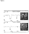
- nano-structured coatings were prepared with example formulations 2 and 3 (Table 3) as described under "Preparation of a coating on a substrate". After the washing step an additional heat treatment was performed at 100°C for 30 minutes on selected samples. An AFM image of a resulting (nano) surface structure for Example I is shown in Figure 3 . Nano scratch tests were performed on such nano-structured coatings as described in the previous Example. An AFM image of a nano-structured coating after scratching is shown in Figure 4 .
- Example 7 Optical properties of nanosurface structured coatings
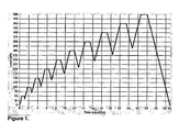
- Nano-structured films were prepared as described under "Preparation of a coating on a substrate", on one side of glass microscope slides from Example formulation 1. Spectral transmission in the visible region of the spectrum was measured with a Perkin-Elmer Lambda-20 UV-Vis spectrometer. The transmission is shown in Figure 5 , together with the transmission of the uncoated glass slide. The transmission clearly increases by application of the single nano-structured coating.
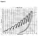
- Nano-structured films were prepared as described under "Preparation of a coating on a substrate", on a silicon wafer and on both sides of a glass microscope slide from comparative Example formulation 4 (see Table 7).
- An AFM image of a resulting surface structure is given in Figure 7 .
- Spectral transmission in the visible region of the spectrum was measured with a Perkin-Elmer Lambda -20 UV-Vis spectrometer. The transmission is shown in Figure 8 , together with the transmission of the uncoated glass slide. The transmission increases by application of the single nano-structured coating.
- Table 7 Formulations used for the comparative examples Example Formulation no.
Landscapes
- Physics & Mathematics (AREA)
- General Physics & Mathematics (AREA)
- Optics & Photonics (AREA)
- Chemical & Material Sciences (AREA)
- Engineering & Computer Science (AREA)
- Nanotechnology (AREA)
- Crystallography & Structural Chemistry (AREA)
- Materials Engineering (AREA)
- Condensed Matter Physics & Semiconductors (AREA)
- Composite Materials (AREA)
- Inorganic Chemistry (AREA)
- Paints Or Removers (AREA)
- Application Of Or Painting With Fluid Materials (AREA)
- Surface Treatment Of Optical Elements (AREA)
- Laminated Bodies (AREA)
- Coating Of Shaped Articles Made Of Macromolecular Substances (AREA)
Claims (10)
- Verfahren zur Herstellung einer einschichtigen Kratzschutzbeschichtung (Hard Coat), umfassend die Schritte:a) Auftragen eines Gemischs auf ein Substrat, wobei das Gemisch Folgendes umfasst:i. wenigstens ein erstes Material, das unter den in Schritt b) gewählten Bedingungen nicht vernetzt, wobei es sich bei dem ersten Material um Hydroxypropylcellulose handelt;ii. wenigstens ein zweites Material, das unter den in Schritt b) gewählten Bedingungen vernetzt;iii. Nanoteilchen; undiv. gegebenenfalls wenigstens ein Lösungsmittel;b) Induzieren der Vernetzung in dem auf das Substrat aufgetragenen Gemisch;c) anschließend Entfernen wenigstens eines Teils des ersten Materials.
- Verfahren gemäß Anspruch 1, wobei das Gemisch vor dem Vernetzen homogen ist.
- Verfahren gemäß Anspruch 1 oder 2, wobei wenigstens ein Teil der Nanoteilchen organische Gruppen auf ihrer Oberfläche aufweisen.
- Verfahren gemäß einem der Ansprüche 1 bis 3, wobei wenigstens ein Teil der Nanoteilchen vernetzende Gruppen auf ihrer Oberfläche aufweisen.
- Verfahren gemäß einem der Ansprüche 1 bis 4, wobei die Nanoteilchen anorganische Nanoteilchen sind.
- Verfahren gemäß Anspruch 5, wobei die Nanoteilchen Oxidteilchen sind, wobei das Oxid aus der Gruppe ausgewählt ist, die aus Aluminiumoxid, Siliciumoxid, Zirconiumoxid, Titanoxid, Antimonoxid, Zinkoxid, Zinnoxid, Indiumoxid und Ceroxid besteht.
- Verfahren gemäß einem der Ansprüche 1 bis 6, wobei das in dem zweiten Material vorhandene Monomer oder Oligomer wenigstens zwei, vorzugsweise drei oder mehr, reaktive/polymerisierbare oder vernetzungsfähige Gruppen pro Monomer- oder Oligomermolekül aufweist.
- Verfahren gemäß einem der Ansprüche 1 bis 7, wobei die Mehrzahl der Nanoteilchen einen Durchmesser von weniger als 400 nm und vorzugsweise weniger als 50 nm aufweist.
- Verfahren gemäß einem der Ansprüche 1 bis 8, wobei das auf das Substrat aufgetragene Gemisch während oder nach dem Vernetzen erhitzt wird.
- Verfahren gemäß einem der Ansprüche 1 bis 9, wobei das Gemisch wenigstens ein Lösungsmittel umfasst, das aus der Gruppe ausgewählt ist, die aus 1,4-Dioxan, Aceton, Acetonitril, Chloroform, Chlorphenol, Cyclohexan, Cyclohexanon, Cyclopentanon, Dichlormethan, Diethylacetat, Diethylketon, Dimethylcarbonat, Dimethylformamid, Dimethylsulfoxid, Ethanol, Ethylacetat, m-Kresol, mono- und dialkylsubstituierten Glycolen, N,N-Dimethylacetamid, p-Chlorphenol, 1,2-Propandiol, 1-Pentanol, 1-Propanol, 2-Hexanon, 2-Methoxyethanol, 2-Methyl-2-propanol, 2-Octanon, 2-Propanol, 3-Pentanon, 4-Methyl-2-pentanon, Hexafluorisopropanol, Methanol, Methylacetat, Methylacetoacetat, Methylethylketon, Methylpropylketon, n-Methylpyrrolidon-2, n-Pentylacetat, Phenol, Tetrafluor-n-propanol, Tetrafluorisopropanol, Tetrahydrofuran, Toluol, Xylol und Wasser besteht.
Priority Applications (2)
| Application Number | Priority Date | Filing Date | Title |
|---|---|---|---|
| EP03772952A EP1558949B1 (de) | 2002-11-06 | 2003-11-04 | Verfahren zur herstellung einer mechanisch haltbaren einlagigen beschichtung mit anti-reflex eigenschaften |
| EP20090158688 EP2081057A3 (de) | 2002-11-06 | 2003-11-04 | Mechanisch beständige Einzelbeschichtung mit Entspiegelungseigenschaften |
Applications Claiming Priority (4)
| Application Number | Priority Date | Filing Date | Title |
|---|---|---|---|
| EP20020079649 EP1418448A1 (de) | 2002-11-06 | 2002-11-06 | Herstellung einer mechanisch haltbaren, einlagigen Beschichtung mit Antireflex-Eigenschaften |
| EP02079649 | 2002-11-06 | ||
| EP03772952A EP1558949B1 (de) | 2002-11-06 | 2003-11-04 | Verfahren zur herstellung einer mechanisch haltbaren einlagigen beschichtung mit anti-reflex eigenschaften |
| PCT/NL2003/000770 WO2004042434A1 (en) | 2002-11-06 | 2003-11-04 | Preparation of a mechanically durable single layer coating with anti-reflective properties |
Related Child Applications (1)
| Application Number | Title | Priority Date | Filing Date |
|---|---|---|---|
| EP20090158688 Division EP2081057A3 (de) | 2002-11-06 | 2003-11-04 | Mechanisch beständige Einzelbeschichtung mit Entspiegelungseigenschaften |
Publications (2)
| Publication Number | Publication Date |
|---|---|
| EP1558949A1 EP1558949A1 (de) | 2005-08-03 |
| EP1558949B1 true EP1558949B1 (de) | 2009-08-05 |
Family
ID=32103978
Family Applications (3)
| Application Number | Title | Priority Date | Filing Date |
|---|---|---|---|
| EP20020079649 Withdrawn EP1418448A1 (de) | 2002-11-06 | 2002-11-06 | Herstellung einer mechanisch haltbaren, einlagigen Beschichtung mit Antireflex-Eigenschaften |
| EP20090158688 Withdrawn EP2081057A3 (de) | 2002-11-06 | 2003-11-04 | Mechanisch beständige Einzelbeschichtung mit Entspiegelungseigenschaften |
| EP03772952A Expired - Lifetime EP1558949B1 (de) | 2002-11-06 | 2003-11-04 | Verfahren zur herstellung einer mechanisch haltbaren einlagigen beschichtung mit anti-reflex eigenschaften |
Family Applications Before (2)
| Application Number | Title | Priority Date | Filing Date |
|---|---|---|---|
| EP20020079649 Withdrawn EP1418448A1 (de) | 2002-11-06 | 2002-11-06 | Herstellung einer mechanisch haltbaren, einlagigen Beschichtung mit Antireflex-Eigenschaften |
| EP20090158688 Withdrawn EP2081057A3 (de) | 2002-11-06 | 2003-11-04 | Mechanisch beständige Einzelbeschichtung mit Entspiegelungseigenschaften |
Country Status (10)
| Country | Link |
|---|---|
| US (2) | US7655298B2 (de) |
| EP (3) | EP1418448A1 (de) |
| JP (1) | JP4589725B2 (de) |
| KR (1) | KR100771739B1 (de) |
| CN (1) | CN100432706C (de) |
| AT (1) | ATE438871T1 (de) |
| AU (1) | AU2003279613A1 (de) |
| DE (1) | DE60328703D1 (de) |
| TW (1) | TWI314589B (de) |
| WO (1) | WO2004042434A1 (de) |
Families Citing this family (57)
| Publication number | Priority date | Publication date | Assignee | Title |
|---|---|---|---|---|
| US7442629B2 (en) * | 2004-09-24 | 2008-10-28 | President & Fellows Of Harvard College | Femtosecond laser-induced formation of submicrometer spikes on a semiconductor substrate |
| US7074463B2 (en) | 2003-09-12 | 2006-07-11 | 3M Innovative Properties Company | Durable optical element |
| US7282272B2 (en) * | 2003-09-12 | 2007-10-16 | 3M Innovative Properties Company | Polymerizable compositions comprising nanoparticles |
| US7170666B2 (en) | 2004-07-27 | 2007-01-30 | Hewlett-Packard Development Company, L.P. | Nanostructure antireflection surfaces |
| US7326448B2 (en) | 2005-02-17 | 2008-02-05 | 3M Innovative Properties Company | Polymerizable oligomeric urethane compositions comprising nanoparticles |
| TWI403522B (zh) | 2005-07-01 | 2013-08-01 | Jsr Corp | A hardened resin composition and a hardened film thereof |
| US20070065638A1 (en) * | 2005-09-20 | 2007-03-22 | Eastman Kodak Company | Nano-structured thin film with reduced light reflection |
| CN101253227B (zh) | 2005-10-04 | 2011-05-18 | 日本印帝股份公司 | 具有特定的表面形状与物性的结构体及用于形成该结构体的(甲基)丙烯酸系聚合性组合物 |
| US8067065B2 (en) * | 2005-12-08 | 2011-11-29 | Toyota Motor Engineering & Manufacturing North America, Inc. | Fibrillar, nanotextured coating and method for its manufacture |
| KR100940433B1 (ko) * | 2006-12-29 | 2010-02-10 | 주식회사 엘지화학 | 반사방지 코팅 조성물 및 이것을 이용하여 제조된 반사방지필름 |
| CN101796146B (zh) * | 2007-09-07 | 2013-09-04 | 3M创新有限公司 | 包含经表面改性的高折射率纳米粒子的自组装抗反射涂层 |
| KR20090049518A (ko) * | 2007-11-13 | 2009-05-18 | 주식회사 엘지화학 | 반사방지 코팅 조성물 및 이것을 이용하여 제조된 반사방지필름 |
| KR101009821B1 (ko) * | 2007-11-13 | 2011-01-19 | 주식회사 엘지화학 | 반사방지 코팅 조성물, 반사방지 필름 및 이의 제조방법 |
| EP2228414A1 (de) * | 2009-03-13 | 2010-09-15 | Bayer MaterialScience AG | UV-härtbare, verschleißfeste und antistatische Beschichtung, die mit Kohlenstoffnanoröhrchen gefüllt ist |
| BRPI1006654A2 (pt) | 2009-04-15 | 2016-02-10 | 3M Innovative Properties Co | construções ópticas retrorrefletoras e filmes ópticos |
| US9464179B2 (en) | 2009-04-15 | 2016-10-11 | 3M Innovative Properties Company | Process and apparatus for a nanovoided article |
| US9291752B2 (en) | 2013-08-19 | 2016-03-22 | 3M Innovative Properties Company | Retroreflecting optical construction |
| WO2010120864A1 (en) | 2009-04-15 | 2010-10-21 | 3M Innovative Properties Company | Optical film |
| US8808811B2 (en) | 2009-04-15 | 2014-08-19 | 3M Innovative Properties Company | Process and apparatus for a nanovoided article |
| US9353268B2 (en) | 2009-04-30 | 2016-05-31 | Enki Technology, Inc. | Anti-reflective and anti-soiling coatings for self-cleaning properties |
| US9376593B2 (en) | 2009-04-30 | 2016-06-28 | Enki Technology, Inc. | Multi-layer coatings |
| US8864897B2 (en) | 2009-04-30 | 2014-10-21 | Enki Technology, Inc. | Anti-reflective and anti-soiling coatings with self-cleaning properties |
| JP2011225846A (ja) * | 2010-03-31 | 2011-11-10 | Fujifilm Corp | ハードコート層形成用組成物、光学フィルム、光学フィルムの製造方法、偏光板、及び画像表示装置 |
| JP5997132B2 (ja) | 2010-04-15 | 2016-09-28 | スリーエム イノベイティブ プロパティズ カンパニー | 再帰反射性物品及びその形成方法 |
| MX341955B (es) | 2010-04-15 | 2016-09-08 | 3M Innovative Properties Co | Articulos retrorreflectantes que incluyen areas opticamente activas y areas opticamente inactivas. |
| WO2011129831A1 (en) | 2010-04-15 | 2011-10-20 | 3M Innovative Properties Company | Retroreflective articles including optically active areas and optically inactive areas |
| EP2431422A3 (de) | 2010-09-21 | 2013-07-10 | Rohm and Haas Company | IR-reflektierende Zusammensetzungen |
| EP2431423A3 (de) | 2010-09-21 | 2013-07-10 | Rohm and Haas Company | Antireflexionsbeschichtungen |
| EP2431424A3 (de) | 2010-09-21 | 2014-03-05 | Rohm and Haas Company | UV-reflektierende Zusammensetzungen |
| WO2012133339A1 (ja) | 2011-03-29 | 2012-10-04 | 凸版印刷株式会社 | 反射防止フィルム及び偏光板 |
| JP6199864B2 (ja) | 2011-08-17 | 2017-09-20 | スリーエム イノベイティブ プロパティズ カンパニー | ナノ構造物品及びそれを製造するための方法 |
| JP2015501449A (ja) * | 2011-10-25 | 2015-01-15 | ユニピクセル ディスプレイズ,インコーポレーテッド | ディスプレイデバイス用のフレキシブルな耐スクラッチ性フィルム |
| KR20140096307A (ko) | 2011-10-25 | 2014-08-05 | 유니-픽셀 디스플레이스, 인코포레이티드 | 긁힘 방지 터치 센서 |
| US8668960B1 (en) | 2013-02-08 | 2014-03-11 | Enki Technology, Inc. | Flow coating apparatus and method of coating |
| WO2014168188A1 (ja) * | 2013-04-10 | 2014-10-16 | 三井化学株式会社 | 積層体 |
| US9366784B2 (en) | 2013-05-07 | 2016-06-14 | Corning Incorporated | Low-color scratch-resistant articles with a multilayer optical film |
| US9110230B2 (en) | 2013-05-07 | 2015-08-18 | Corning Incorporated | Scratch-resistant articles with retained optical properties |
| US9684097B2 (en) | 2013-05-07 | 2017-06-20 | Corning Incorporated | Scratch-resistant articles with retained optical properties |
| US9703011B2 (en) | 2013-05-07 | 2017-07-11 | Corning Incorporated | Scratch-resistant articles with a gradient layer |
| US9359261B2 (en) | 2013-05-07 | 2016-06-07 | Corning Incorporated | Low-color scratch-resistant articles with a multilayer optical film |
| CN103353626B (zh) * | 2013-06-13 | 2016-04-20 | 北京大学深圳研究生院 | 三维光栅抗反射结构和元器件 |
| JP6326801B2 (ja) * | 2013-12-12 | 2018-05-23 | 大日本印刷株式会社 | 積層体 |
| CN109263151B (zh) | 2013-12-19 | 2021-02-05 | 3M创新有限公司 | 多层复合材料制品 |
| WO2015122641A1 (ko) * | 2014-02-13 | 2015-08-20 | 전자부품연구원 | 발열 페이스트 조성물, 이를 이용한 면상 발열체 소자 및 휴대용 저전력 발열 히터 |
| US9335444B2 (en) | 2014-05-12 | 2016-05-10 | Corning Incorporated | Durable and scratch-resistant anti-reflective articles |
| US11267973B2 (en) | 2014-05-12 | 2022-03-08 | Corning Incorporated | Durable anti-reflective articles |
| WO2015200003A1 (en) | 2014-06-23 | 2015-12-30 | 3M Innovative Properties Company | Silicon-containing polymer and method of making a silicon-containing polymer |
| US9598586B2 (en) | 2014-07-14 | 2017-03-21 | Enki Technology, Inc. | Coating materials and methods for enhanced reliability |
| US9382449B2 (en) | 2014-09-19 | 2016-07-05 | Enki Technology, Inc. | Optical enhancing durable anti-reflective coating |
| US9376589B2 (en) | 2014-07-14 | 2016-06-28 | Enki Technology, Inc. | High gain durable anti-reflective coating with oblate voids |
| US9790593B2 (en) | 2014-08-01 | 2017-10-17 | Corning Incorporated | Scratch-resistant materials and articles including the same |
| JP2018536177A (ja) | 2015-09-14 | 2018-12-06 | コーニング インコーポレイテッド | 高光線透過性かつ耐擦傷性反射防止物品 |
| US10510985B2 (en) * | 2016-06-14 | 2019-12-17 | Motorola Mobility Llc | Polymer hard coat and methods of preparation |
| CN114085037B (zh) | 2018-08-17 | 2023-11-10 | 康宁股份有限公司 | 具有薄的耐久性减反射结构的无机氧化物制品 |
| US20200339828A1 (en) * | 2019-04-26 | 2020-10-29 | Canon Kabushiki Kaisha | Photocurable composition |
| US11554575B2 (en) | 2020-06-24 | 2023-01-17 | Motorola Mobility Llc | Composite display cover |
| US12386101B2 (en) | 2020-07-09 | 2025-08-12 | Corning Incorporated | Textured region of a substrate to reduce specular reflectance incorporating surface features with an elliptical perimeter or segments thereof, and method of making the same |
Family Cites Families (19)
| Publication number | Priority date | Publication date | Assignee | Title |
|---|---|---|---|---|
| US3783075A (en) * | 1967-03-10 | 1974-01-01 | Polaroid Corp | Method of manufacturing photographic film unit |
| DE2555783C3 (de) * | 1975-12-11 | 1979-05-31 | Hoechst Ag, 6000 Frankfurt | Haftmasse |
| JPS61170702A (ja) * | 1985-01-25 | 1986-08-01 | Kunio Yoshida | 光学薄膜の製作方法 |
| JP2613436B2 (ja) * | 1988-06-10 | 1997-05-28 | 旭光学工業株式会社 | プラスチックレンズ用反射防止膜の形成方法 |
| DE69124410T2 (de) * | 1990-04-18 | 1997-07-10 | Matsushita Electric Ind Co Ltd | Kompositschicht, Glaskompositmaterial und Verfahren zu seiner Herstellung |
| JPH04121701A (ja) * | 1990-09-12 | 1992-04-22 | Canon Inc | 反射防止膜 |
| JPH05181002A (ja) * | 1992-01-07 | 1993-07-23 | Nippon Sheet Glass Co Ltd | 低反射物品およびその製造方法 |
| US5523649A (en) | 1994-11-08 | 1996-06-04 | Chunghwa Picture Tubes, Ltd. | Multilayer antireflective coating for video display panel |
| EP0881192B1 (de) | 1997-05-26 | 2002-03-27 | Nissan Chemical Industries, Ltd. | Verfahren zur Herstellung eines hydrophoben Kieselsäure Organosols |
| US6589650B1 (en) * | 2000-08-07 | 2003-07-08 | 3M Innovative Properties Company | Microscope cover slip materials |
| US6323255B1 (en) | 1998-09-30 | 2001-11-27 | Dsm N.V. | Radiation-curable composition |
| JP2000147258A (ja) * | 1998-11-17 | 2000-05-26 | Daicel Chem Ind Ltd | 選択反射性成形体 |
| CN1235985C (zh) * | 1998-12-09 | 2006-01-11 | 日本化药株式会社 | 硬涂覆材料以及用该材料获得的膜 |
| HK1044960A1 (zh) * | 1999-10-19 | 2002-11-08 | Rolic Ag | 拓撲結構化的聚合物塗層 |
| US6686031B2 (en) * | 2000-02-23 | 2004-02-03 | Fuji Photo Film Co., Ltd. | Hard coat film and display device having same |
| JP2002139601A (ja) * | 2000-11-06 | 2002-05-17 | Canon Inc | 反射防止膜、及びその製造方法 |
| ATE350677T1 (de) * | 2000-11-14 | 2007-01-15 | Cpfilms Inc | Optisch aktive schichtzusammensetzung |
| JP2002286906A (ja) * | 2001-03-23 | 2002-10-03 | Mitsubishi Chemicals Corp | 反射防止方法及び反射防止構造並びに反射防止構造を有する反射防止構造体及びその製造方法 |
| WO2003022935A1 (en) * | 2001-09-11 | 2003-03-20 | 3M Innovative Properties Company | Smudge resistant nanocomposite hardcoats and methods for making same |
-
2002
- 2002-11-06 EP EP20020079649 patent/EP1418448A1/de not_active Withdrawn
-
2003
- 2003-11-04 EP EP20090158688 patent/EP2081057A3/de not_active Withdrawn
- 2003-11-04 JP JP2004549714A patent/JP4589725B2/ja not_active Expired - Fee Related
- 2003-11-04 EP EP03772952A patent/EP1558949B1/de not_active Expired - Lifetime
- 2003-11-04 KR KR1020057008106A patent/KR100771739B1/ko not_active Expired - Fee Related
- 2003-11-04 CN CNB2003801028502A patent/CN100432706C/zh not_active Expired - Fee Related
- 2003-11-04 WO PCT/NL2003/000770 patent/WO2004042434A1/en not_active Ceased
- 2003-11-04 US US10/533,094 patent/US7655298B2/en not_active Expired - Fee Related
- 2003-11-04 AU AU2003279613A patent/AU2003279613A1/en not_active Abandoned
- 2003-11-04 DE DE60328703T patent/DE60328703D1/de not_active Expired - Lifetime
- 2003-11-04 AT AT03772952T patent/ATE438871T1/de not_active IP Right Cessation
- 2003-11-06 TW TW92131118A patent/TWI314589B/zh active
-
2008
- 2008-12-31 US US12/318,594 patent/US20090191346A1/en not_active Abandoned
Also Published As
| Publication number | Publication date |
|---|---|
| EP1418448A1 (de) | 2004-05-12 |
| EP2081057A3 (de) | 2012-07-04 |
| KR20050074985A (ko) | 2005-07-19 |
| TW200419007A (en) | 2004-10-01 |
| US20060014012A1 (en) | 2006-01-19 |
| US20090191346A1 (en) | 2009-07-30 |
| KR100771739B1 (ko) | 2007-10-30 |
| WO2004042434A1 (en) | 2004-05-21 |
| CN1711486A (zh) | 2005-12-21 |
| DE60328703D1 (de) | 2009-09-17 |
| US7655298B2 (en) | 2010-02-02 |
| EP1558949A1 (de) | 2005-08-03 |
| EP2081057A2 (de) | 2009-07-22 |
| JP2006505395A (ja) | 2006-02-16 |
| AU2003279613A1 (en) | 2004-06-07 |
| JP4589725B2 (ja) | 2010-12-01 |
| CN100432706C (zh) | 2008-11-12 |
| TWI314589B (en) | 2009-09-11 |
| ATE438871T1 (de) | 2009-08-15 |
Similar Documents
| Publication | Publication Date | Title |
|---|---|---|
| EP1558949B1 (de) | Verfahren zur herstellung einer mechanisch haltbaren einlagigen beschichtung mit anti-reflex eigenschaften | |
| EP1479734B1 (de) | Verfahren zur Herstellung von Nanostrukturierten Oberflächenbeschichtungen, deren Beschichtungen und Gegenständen enthaltend die Beschichtung | |
| EP1479738A1 (de) | Hydrophobe Beschichtungen enthaltend reaktive Nanopartikel | |
| KR101918682B1 (ko) | 저굴절층 및 이를 포함하는 반사 방지 필름 | |
| KR20080045226A (ko) | 광 반사가 감소된 나노-구조화된 박막 | |
| EP3346302B1 (de) | Niedrigbrechende schicht und dieselbe umfassende antireflexfolie | |
| JP4362509B2 (ja) | 反射防止フィルムおよびその製造方法 | |
| JPWO2019003905A1 (ja) | 反射防止フィルム、偏光板、及び画像表示装置 | |
| EP1674891A1 (de) | Antireflektionsschicht, Verfahren zu seiner Herstellung und diese enthaltende Gegenstände | |
| US20080047748A1 (en) | Object Comprising A Non-Insulative Coating | |
| WO2017030392A1 (ko) | 저굴절층 및 이를 포함하는 반사 방지 필름 | |
| WO2017030391A1 (ko) | 저굴절층 및 이를 포함하는 반사 방지 필름 |
Legal Events
| Date | Code | Title | Description |
|---|---|---|---|
| PUAI | Public reference made under article 153(3) epc to a published international application that has entered the european phase |
Free format text: ORIGINAL CODE: 0009012 |
|
| 17P | Request for examination filed |
Effective date: 20050408 |
|
| AK | Designated contracting states |
Kind code of ref document: A1 Designated state(s): AT BE BG CH CY CZ DE DK EE ES FI FR GB GR HU IE IT LI LU MC NL PT RO SE SI SK TR |
|
| AX | Request for extension of the european patent |
Extension state: AL LT LV MK |
|
| DAX | Request for extension of the european patent (deleted) | ||
| 17Q | First examination report despatched |
Effective date: 20060509 |
|
| GRAP | Despatch of communication of intention to grant a patent |
Free format text: ORIGINAL CODE: EPIDOSNIGR1 |
|
| RTI1 | Title (correction) |
Free format text: METHOD FOR PREPARATION OF A MECHANICALLY DURABLE SINGLE LAYER COATING WITH ANTI-REFLECTIVE PROPERTIES |
|
| GRAS | Grant fee paid |
Free format text: ORIGINAL CODE: EPIDOSNIGR3 |
|
| GRAA | (expected) grant |
Free format text: ORIGINAL CODE: 0009210 |
|
| AK | Designated contracting states |
Kind code of ref document: B1 Designated state(s): AT BE BG CH CY CZ DE DK EE ES FI FR GB GR HU IE IT LI LU MC NL PT RO SE SI SK TR |
|
| REG | Reference to a national code |
Ref country code: GB Ref legal event code: FG4D |
|
| REG | Reference to a national code |
Ref country code: CH Ref legal event code: EP |
|
| REG | Reference to a national code |
Ref country code: IE Ref legal event code: FG4D |
|
| REF | Corresponds to: |
Ref document number: 60328703 Country of ref document: DE Date of ref document: 20090917 Kind code of ref document: P |
|
| PG25 | Lapsed in a contracting state [announced via postgrant information from national office to epo] |
Ref country code: ES Free format text: LAPSE BECAUSE OF FAILURE TO SUBMIT A TRANSLATION OF THE DESCRIPTION OR TO PAY THE FEE WITHIN THE PRESCRIBED TIME-LIMIT Effective date: 20091116 Ref country code: SE Free format text: LAPSE BECAUSE OF FAILURE TO SUBMIT A TRANSLATION OF THE DESCRIPTION OR TO PAY THE FEE WITHIN THE PRESCRIBED TIME-LIMIT Effective date: 20090805 Ref country code: FI Free format text: LAPSE BECAUSE OF FAILURE TO SUBMIT A TRANSLATION OF THE DESCRIPTION OR TO PAY THE FEE WITHIN THE PRESCRIBED TIME-LIMIT Effective date: 20090805 Ref country code: AT Free format text: LAPSE BECAUSE OF FAILURE TO SUBMIT A TRANSLATION OF THE DESCRIPTION OR TO PAY THE FEE WITHIN THE PRESCRIBED TIME-LIMIT Effective date: 20090805 |
|
| NLV1 | Nl: lapsed or annulled due to failure to fulfill the requirements of art. 29p and 29m of the patents act | ||
| PG25 | Lapsed in a contracting state [announced via postgrant information from national office to epo] |
Ref country code: NL Free format text: LAPSE BECAUSE OF FAILURE TO SUBMIT A TRANSLATION OF THE DESCRIPTION OR TO PAY THE FEE WITHIN THE PRESCRIBED TIME-LIMIT Effective date: 20090805 Ref country code: SI Free format text: LAPSE BECAUSE OF FAILURE TO SUBMIT A TRANSLATION OF THE DESCRIPTION OR TO PAY THE FEE WITHIN THE PRESCRIBED TIME-LIMIT Effective date: 20090805 |
|
| PG25 | Lapsed in a contracting state [announced via postgrant information from national office to epo] |
Ref country code: PT Free format text: LAPSE BECAUSE OF FAILURE TO SUBMIT A TRANSLATION OF THE DESCRIPTION OR TO PAY THE FEE WITHIN THE PRESCRIBED TIME-LIMIT Effective date: 20091205 Ref country code: BG Free format text: LAPSE BECAUSE OF FAILURE TO SUBMIT A TRANSLATION OF THE DESCRIPTION OR TO PAY THE FEE WITHIN THE PRESCRIBED TIME-LIMIT Effective date: 20091105 |
|
| PG25 | Lapsed in a contracting state [announced via postgrant information from national office to epo] |
Ref country code: CZ Free format text: LAPSE BECAUSE OF FAILURE TO SUBMIT A TRANSLATION OF THE DESCRIPTION OR TO PAY THE FEE WITHIN THE PRESCRIBED TIME-LIMIT Effective date: 20090805 Ref country code: RO Free format text: LAPSE BECAUSE OF FAILURE TO SUBMIT A TRANSLATION OF THE DESCRIPTION OR TO PAY THE FEE WITHIN THE PRESCRIBED TIME-LIMIT Effective date: 20090805 Ref country code: DK Free format text: LAPSE BECAUSE OF FAILURE TO SUBMIT A TRANSLATION OF THE DESCRIPTION OR TO PAY THE FEE WITHIN THE PRESCRIBED TIME-LIMIT Effective date: 20090805 Ref country code: EE Free format text: LAPSE BECAUSE OF FAILURE TO SUBMIT A TRANSLATION OF THE DESCRIPTION OR TO PAY THE FEE WITHIN THE PRESCRIBED TIME-LIMIT Effective date: 20090805 |
|
| PG25 | Lapsed in a contracting state [announced via postgrant information from national office to epo] |
Ref country code: SK Free format text: LAPSE BECAUSE OF FAILURE TO SUBMIT A TRANSLATION OF THE DESCRIPTION OR TO PAY THE FEE WITHIN THE PRESCRIBED TIME-LIMIT Effective date: 20090805 |
|
| PLBE | No opposition filed within time limit |
Free format text: ORIGINAL CODE: 0009261 |
|
| STAA | Information on the status of an ep patent application or granted ep patent |
Free format text: STATUS: NO OPPOSITION FILED WITHIN TIME LIMIT |
|
| PG25 | Lapsed in a contracting state [announced via postgrant information from national office to epo] |
Ref country code: MC Free format text: LAPSE BECAUSE OF NON-PAYMENT OF DUE FEES Effective date: 20091130 Ref country code: BE Free format text: LAPSE BECAUSE OF FAILURE TO SUBMIT A TRANSLATION OF THE DESCRIPTION OR TO PAY THE FEE WITHIN THE PRESCRIBED TIME-LIMIT Effective date: 20090805 |
|
| REG | Reference to a national code |
Ref country code: CH Ref legal event code: PL |
|
| 26N | No opposition filed |
Effective date: 20100507 |
|
| GBPC | Gb: european patent ceased through non-payment of renewal fee |
Effective date: 20091105 |
|
| PG25 | Lapsed in a contracting state [announced via postgrant information from national office to epo] |
Ref country code: LI Free format text: LAPSE BECAUSE OF NON-PAYMENT OF DUE FEES Effective date: 20091130 Ref country code: IE Free format text: LAPSE BECAUSE OF NON-PAYMENT OF DUE FEES Effective date: 20091104 Ref country code: GR Free format text: LAPSE BECAUSE OF FAILURE TO SUBMIT A TRANSLATION OF THE DESCRIPTION OR TO PAY THE FEE WITHIN THE PRESCRIBED TIME-LIMIT Effective date: 20091106 Ref country code: CH Free format text: LAPSE BECAUSE OF NON-PAYMENT OF DUE FEES Effective date: 20091130 |
|
| PG25 | Lapsed in a contracting state [announced via postgrant information from national office to epo] |
Ref country code: GB Free format text: LAPSE BECAUSE OF NON-PAYMENT OF DUE FEES Effective date: 20091105 |
|
| PG25 | Lapsed in a contracting state [announced via postgrant information from national office to epo] |
Ref country code: IT Free format text: LAPSE BECAUSE OF FAILURE TO SUBMIT A TRANSLATION OF THE DESCRIPTION OR TO PAY THE FEE WITHIN THE PRESCRIBED TIME-LIMIT Effective date: 20090805 |
|
| PG25 | Lapsed in a contracting state [announced via postgrant information from national office to epo] |
Ref country code: LU Free format text: LAPSE BECAUSE OF NON-PAYMENT OF DUE FEES Effective date: 20091104 |
|
| PG25 | Lapsed in a contracting state [announced via postgrant information from national office to epo] |
Ref country code: HU Free format text: LAPSE BECAUSE OF FAILURE TO SUBMIT A TRANSLATION OF THE DESCRIPTION OR TO PAY THE FEE WITHIN THE PRESCRIBED TIME-LIMIT Effective date: 20100206 |
|
| PG25 | Lapsed in a contracting state [announced via postgrant information from national office to epo] |
Ref country code: TR Free format text: LAPSE BECAUSE OF FAILURE TO SUBMIT A TRANSLATION OF THE DESCRIPTION OR TO PAY THE FEE WITHIN THE PRESCRIBED TIME-LIMIT Effective date: 20090805 |
|
| PG25 | Lapsed in a contracting state [announced via postgrant information from national office to epo] |
Ref country code: CY Free format text: LAPSE BECAUSE OF FAILURE TO SUBMIT A TRANSLATION OF THE DESCRIPTION OR TO PAY THE FEE WITHIN THE PRESCRIBED TIME-LIMIT Effective date: 20090805 |
|
| REG | Reference to a national code |
Ref country code: FR Ref legal event code: PLFP Year of fee payment: 13 |
|
| REG | Reference to a national code |
Ref country code: FR Ref legal event code: PLFP Year of fee payment: 14 |
|
| REG | Reference to a national code |
Ref country code: FR Ref legal event code: PLFP Year of fee payment: 15 |
|
| PGFP | Annual fee paid to national office [announced via postgrant information from national office to epo] |
Ref country code: FR Payment date: 20170918 Year of fee payment: 15 |
|
| PGFP | Annual fee paid to national office [announced via postgrant information from national office to epo] |
Ref country code: DE Payment date: 20171031 Year of fee payment: 15 |
|
| REG | Reference to a national code |
Ref country code: DE Ref legal event code: R119 Ref document number: 60328703 Country of ref document: DE |
|
| PG25 | Lapsed in a contracting state [announced via postgrant information from national office to epo] |
Ref country code: DE Free format text: LAPSE BECAUSE OF NON-PAYMENT OF DUE FEES Effective date: 20190601 Ref country code: FR Free format text: LAPSE BECAUSE OF NON-PAYMENT OF DUE FEES Effective date: 20181130 |