EP1557487B1 - Verfahren zur Herstellung eines Substrats aus GaN-Kristall - Google Patents
Verfahren zur Herstellung eines Substrats aus GaN-Kristall Download PDFInfo
- Publication number
- EP1557487B1 EP1557487B1 EP05000403A EP05000403A EP1557487B1 EP 1557487 B1 EP1557487 B1 EP 1557487B1 EP 05000403 A EP05000403 A EP 05000403A EP 05000403 A EP05000403 A EP 05000403A EP 1557487 B1 EP1557487 B1 EP 1557487B1
- Authority
- EP
- European Patent Office
- Prior art keywords
- gan crystal
- substrate
- growth
- gan
- crystal
- Prior art date
- Legal status (The legal status is an assumption and is not a legal conclusion. Google has not performed a legal analysis and makes no representation as to the accuracy of the status listed.)
- Expired - Lifetime
Links
Images



Classifications
-
- C—CHEMISTRY; METALLURGY
- C30—CRYSTAL GROWTH
- C30B—SINGLE-CRYSTAL GROWTH; UNIDIRECTIONAL SOLIDIFICATION OF EUTECTIC MATERIAL OR UNIDIRECTIONAL DEMIXING OF EUTECTOID MATERIAL; REFINING BY ZONE-MELTING OF MATERIAL; PRODUCTION OF A HOMOGENEOUS POLYCRYSTALLINE MATERIAL WITH DEFINED STRUCTURE; SINGLE CRYSTALS OR HOMOGENEOUS POLYCRYSTALLINE MATERIAL WITH DEFINED STRUCTURE; AFTER-TREATMENT OF SINGLE CRYSTALS OR A HOMOGENEOUS POLYCRYSTALLINE MATERIAL WITH DEFINED STRUCTURE; APPARATUS THEREFOR
- C30B29/00—Single crystals or homogeneous polycrystalline material with defined structure characterised by the material or by their shape
- C30B29/10—Inorganic compounds or compositions
- C30B29/40—AIIIBV compounds wherein A is B, Al, Ga, In or Tl and B is N, P, As, Sb or Bi
- C30B29/403—AIII-nitrides
- C30B29/406—Gallium nitride
-
- H—ELECTRICITY
- H10—SEMICONDUCTOR DEVICES; ELECTRIC SOLID-STATE DEVICES NOT OTHERWISE PROVIDED FOR
- H10P—GENERIC PROCESSES OR APPARATUS FOR THE MANUFACTURE OR TREATMENT OF DEVICES COVERED BY CLASS H10
- H10P58/00—Singulating wafers or substrates into multiple chips, i.e. dicing
-
- C—CHEMISTRY; METALLURGY
- C30—CRYSTAL GROWTH
- C30B—SINGLE-CRYSTAL GROWTH; UNIDIRECTIONAL SOLIDIFICATION OF EUTECTIC MATERIAL OR UNIDIRECTIONAL DEMIXING OF EUTECTOID MATERIAL; REFINING BY ZONE-MELTING OF MATERIAL; PRODUCTION OF A HOMOGENEOUS POLYCRYSTALLINE MATERIAL WITH DEFINED STRUCTURE; SINGLE CRYSTALS OR HOMOGENEOUS POLYCRYSTALLINE MATERIAL WITH DEFINED STRUCTURE; AFTER-TREATMENT OF SINGLE CRYSTALS OR A HOMOGENEOUS POLYCRYSTALLINE MATERIAL WITH DEFINED STRUCTURE; APPARATUS THEREFOR
- C30B25/00—Single-crystal growth by chemical reaction of reactive gases, e.g. chemical vapour-deposition growth
- C30B25/02—Epitaxial-layer growth
-
- H—ELECTRICITY
- H10—SEMICONDUCTOR DEVICES; ELECTRIC SOLID-STATE DEVICES NOT OTHERWISE PROVIDED FOR
- H10D—INORGANIC ELECTRIC SEMICONDUCTOR DEVICES
- H10D86/00—Integrated devices formed in or on insulating or conducting substrates, e.g. formed in silicon-on-insulator [SOI] substrates or on stainless steel or glass substrates
Definitions
- the present invention relates to methods of manufacturing GaN monocrystalline substrates used in light-emitting devices, such as light-emitting diodes (LEDs) and laser diodes (LDs), made from Group III-V semiconductor compounds.
- LEDs light-emitting diodes
- LDs laser diodes
- GaN-crystal thick films for application as substrates in LEDs, LDs and other light-emitting devices made from Group III-V semiconductor compounds
- one method that has been proposed is, when growing GaN crystal onto a base substrate using a vapor growth technique, to form in the crystal-growth surface pits that define facet planes and to confine the dislocations to, or quench the dislocations along, the boundary lines of the facet planes of the pits, to grow GaN substrates of large area and slight dislocation density.
- EP 1 296 362 A2 relates to a GaN crystal which is grown on the seed implanted undersubstrate by a facet growth method.
- the facet growth makes facet pits above the seeds.
- the facets assemble dislocations to the pit bottoms from neighboring regions and make closed defect accumulating regions (H) under the facet bottoms. Regions (H) arrest dislocations permanently.
- the surrounding regions (Y, Z) are low dislocation density single crystals.
- an object of the present invention is to make available a method of manufacturing GaN crystal substrate that efficiently yields a great amount GaN crystal substrate (that is, in which the substrate-acquisition rate is high) by, in the growing of GaN crystal, inhibiting enlargement of pit size to increase the effective GaN crystal portion in which the grown GaN crystal, separated off in thin, platelike form, is usable as a GaN crystal substrate.
- the present invention provides a method according to claim 1.
- the present invention is a method of manufacturing GaN crystal substrate that includes a further step of forming an aperture-window-defining mask layer onto a growth substrate, and a step of growing GaN crystal by a vapor growth technique onto the mask layer.
- the present invention affords a method of manufacturing GaN crystal substrate in which enlargement of pit size in the growing of GaN crystal is inhibited to enable GaN crystal substrate with a high substrate-acquisition rate to be produced.
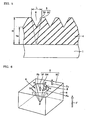
- the GaN-crystal-substrate manufacturing a method includes a step of growing a GaN crystal 4 on a base (growth) substrate 1 by a vapor growth technique.
- a step of growing the GaN crystal 4 pits 6 are formed in a crystal growth face 4A, each pit defining facet planes 5F, and the pit-size increase factor of the pits 6 is made to be 20% or less. By restricting the pit-size increase factor to 20% or less, the pit size is prevented from increasing even when the thickness of the GaN crystal is considerable.
- This result increases the usable thickness He ( ⁇ m) of the GaN crystal, which is the thickness of the GaN crystal that can be separated off as a GaN crystal substrate when the GaN crystal is grown to a thickness H ( ⁇ m), thus improving the substrate acquisition rate-the proportion of usable GaN crystal available from the grown GaN crystal.
- the base substrate herein include, although they are not particularly limited to, a GaN substrate, which is a native substrate that is free from lattice mismatches with the GaN crystal, and foreign substrates that have small lattice mismatches, such as GaAs substrates, sapphire substrates, and SiC substrates.
- the base substrate is not limited to one with a single layer construction; a base substrate on which a GaN layer is formed on a sapphire substrate or SiC substrate, which are foreign substrates, may also be used as a native substrate.
- a foreign substrate such as a sapphire substrate or a SiC substrate
- vapor phase deposition techniques include, but are not particularly limited to, techniques such as HVPE (hydride vapor phase epitaxy), MOCVD (metal-organic chemical vapor deposition), MOC (metal-organic chloride vapor phase epitaxy), and sublimation.
- HVPE hydrogen vapor phase epitaxy
- MOCVD metal-organic chemical vapor deposition
- MOC metal-organic chloride vapor phase epitaxy
- sublimation metal-organic chloride vapor phase epitaxy
- face plane refers to a plane other than the plane that is perpendicular to the crystal growth orientation (growth surface).
- the c-plane 5C is the growth surface since the crystal growth takes place along the c -axis orientation, and the facet planes are those planes other than the c-plane.
- GaN crystal has a hexagonal structure, so the plane, which is the growth surface, is represented as (0001).
- the facet planes that appear frequently are the ⁇ 1 2 12 ⁇ , ⁇ 1 2 11 ⁇ , ⁇ n 2 nnk ⁇ (where n and k are integers), ⁇ 1 1 01 ⁇ , ⁇ 1 1 02 ⁇ , and ⁇ n n 0 k ⁇ (where n and k are integers) planes; among them, the ⁇ 1 2 12 ⁇ plane is a representative example of the facet plane.
- the ⁇ 1 2 12 ⁇ planes include six different planes: the (1 2 12) plane, the (2 11 2) plane, the (11 2 2) plane, the ( 1 2 1 2) plane, the ( 2 112) plane, and the ( 11 22) plane.
- dislocations in the GaN crystal converge in the facet-plane boundaries 5M, and the dislocations (the advancing direction of which is D m ) in the facet plane boundaries 5M further converge in the facet-plane center point 5P, reducing the dislocations elsewhere.
- dislocations having converged in the facet plane boundaries 5M and the facet plane center point 5P are quenched by their interactions with each other, and therefore, the dislocation density reduces as the GaN crystal grows.
- good quality GaN crystal is obtained, with its dislocation density being 1 x 10 7 cm -2 or less.
- facet-plane-defining pits on the crystal growth surface as described above is dependent on crystal growth conditions such as growth temperature, growth rate, and the partial pressure of the precursor gas. For example, the lower the growth temperature is, the more raised the growth rate is, and the more raised the partial pressure of the precursor gas is, the more the formation of the above-noted pits tends to be promoted.
- the growth temperature be about 850°C to 1100°C
- the growth rate be about 50 ⁇ m/hr to 200 ⁇ m/hr
- the GaCl gas partial pressure be about 0.5 kPa to 4 kPa
- the NH 3 gas partial pressure be about 5 kPa to 50 kPa.
- the pit-size increase factor of the above-described pits is rendered20% or less.
- Fig. 1 depicts a GaN crystal 4 in which the pit-size increase factor is made to be 20% and Fig. 5 depicts a GaN crystal 4 in which the pit-size increase factor is made to be 40%.
- H the usable thickness He ( ⁇ m) of the GaN crystal that can be removed as a GaN crystal substrate
- the pit-size increase factor be rendered 10% or less.
- the term "pit-size increase factor” means the average value of the pit-size increase factor in the pits that are formed in the crystal growth surface in growing the GaN crystal.
- reasons for the increase in pit diameter include the following: Letting the angle formed by the c-plane and a facet plane be ⁇ , then if the growth rate Vc of the c-plane with respect to the growth rate V F of the facet plane is V C > V F sin ⁇ , and pits that have grown large coalesce to form still larger pits.
- an effective technique to reduce the pit-size increase factor includes both reducing the growth rate of the plane with respect to the growth rate of a facet plane so that V C ⁇ V F sin ⁇ , and not supplying the crystal growth energy at which the pits would coalesce.
- the growth temperature for GaN crystal be 1000°C or lower in the step of growing the GaN crystal. Reducing the growth temperature for the GaN crystal lowers the growth rate of the c-plane with respect to the growth rate of a facet plane and reduces crystal growth energy, which inhibits coalescence of the pits, thereby reducing the pit-size increase factor.
- the pit-size increase factor can easily be made to be 20% or less.
- the growth temperature for the GaN crystal is preferably 950°C or lower, and still more preferably 900°C or lower.
- the growth rate of the GaN crystal be small.
- the growth rate of the GaN crystal should preferably be 150 ⁇ m/hr or less, more preferably 120 ⁇ m/hr or less, and still more preferably 100 ⁇ m/hr or less.
- the GaCl gas partial pressure should preferably be from 0.5 kPa to 2.0 kPa or lower, and more preferably 0.5 kPa to 1.5 kPa.
- the NH 3 gas partial pressure should preferably be 5 kPa to 15 kPa, and more preferably 5 kPa to 10 kPa.
- another method, according to the present invention, of manufacturing a GaN crystal substrate is a method that includes a step of forming on a growth substrate 1 a mask layer 2 that defines aperture windows, and a step of growing a GaN crystal 4 on the mask layer 2 by a vapor growth technique; in the step of growing the GaN crystal 4, pits 6 are formed, each having facet planes 5F in a crystal growth surface 5A and the pit-size increase factor of the pits 6 is made to be 20% or less.
- the GaN crystal By growing a GaN crystal on the mask layer formed on the growth substrate and by having an aperture-window-defining mask layer, the GaN crystal starts to grow from the portions of the growth substrate 1 that are exposed in the aperture windows of the mask layer 2; in this manner, the mask layer functions to suppress the growth of the GaN crystal in the areas that are not exposed in the aperture windows, and the GaN crystal in the remaining areas grows so as to cover the mask layer.
- This method lessens the adverse effects of dislocations in the growth substrate, and further reduces dislocations in the GaN crystal.
- the growth substrate include, but are not particularly limited to, a GaN substrate, which is a native substrate that is free from lattice mismatches with the GaN crystal, and foreign substrates that have small lattice mismatches, such as a sapphire substrate and a SiC substrate.
- a GaN substrate which is a native substrate that is free from lattice mismatches with the GaN crystal
- foreign substrates that have small lattice mismatches, such as a sapphire substrate and a SiC substrate.
- the growth substrate 4 in cases in which a foreign substrate such as a sapphire substrate or a SiC substrate is used as the growth substrate, after the step of forming on the growth substrate 1 an aperture-window-defining mask layer 2 it is preferable to firstly form by vapor deposition a GaN buffer layer 3 that is an amorphous layer of GaN on the growth substrate 1 exposed in the aperture windows of the mask layer 2 ; thereafter, in the step of growing, by a vapor growth technique, the GaN crystal over the aperture-window-defining mask layer 2, it is preferable to grow a GaN crystal 4 by a vapor growth technique over both the GaN buffer layer 3 and the mask layer 2 for the purposes of alleviating lattice mismatches and reducing the dislocation density of the GaN crystal.
- the aperture-window-defining mask layer is formed by coating the growth substrate with a mask material and thereafter forming the aperture windows by photolithography.
- the mask material include SiO 2 and Si 3 N 4 .
- the aperture windows of the mask layer are provided, and it is possible to employ either a dotted pattern or a striped pattern.
- the dotted pattern refers to one in which isolated dots having a circular shape, a square shape, or the like are distributed regularly; when growing the GaN crystal along the c-plane orientation, it is preferable that three adjacent aperture windows be arranged to sit at the vertexes of equilateral triangles.
- the striped pattern refers to one in which a multiplicity of striplike covering portions and aperture window portions are provided alternately.
- the distance S be 2 ⁇ m or greater, and more preferably 4 ⁇ m or greater, from the viewpoint of reducing coalescence of the pits and controlling increase in pit diameter.
- the growing of a GaN crystal 4 was carried out by an HVPE technique using a GaN substrate, which is a native substrate, as a growth substrate 1.
- the HVPE equipment utilized in the present examples was provided with a boat, disposed inside a reactor, in which Ga metal is accommodated, and was configured to enable introducing HCl gas and a carrier gas directed toward the boat, and, with the growth substrate placed below the boat, to enable introducing NH 3 gas and a carrier gas in the vicinity of the growth substrate.
- a heater was provided on the periphery of the reactor so that the boat and the growth substrate could be heated.
- An exhaust port is provided below the reactor, and the pressure is reduced by a vacuum pump.
- a Ga melt in the boat that is heated at 850°C or higher reacts with the HCl gas, creating a GaCl gas, which reacts with the NH 3 gas, making it possible to grow a GaN crystal on the growth substrate.
- the carrier gas used here was a H 2 gas.
- GaN crystals were grown to a thickness of about 2 mm on growth substrates at the growth temperatures, GaCl partial pressures, NH 3 partial pressures, and growth rates set forth in Table I. Then, the GaN crystals were sliced with a wire saw or an internal-diameter saw and the surfaces were polished to obtain GaN crystal substrates of predetermined thickness. The dislocation densities, pit-size increase factors, and substrate acquisition rate of the GaN crystals are summarized in Table I.
- aperture-window-defining mask layers 2 were formed on the growth substrates, followed by growing GaN crystals 4 over the mask layers 2 by an HVPE technique.
- Each aperture-window-defining mask layer was formed by forming a 100 nm-thick SiO 2 layer by CVD, and thereafter forming by photolithography aperture windows that are arrayed in a dotted pattern in which three adjacent aperture windows (squares 2 ⁇ m to a side) sit at the vertexes of equilateral triangles (the distance between the adjacent aperture windows being 4 ⁇ m).
- GaN crystals were grown to a thickness of about 2 mm on growth substrates at the growth temperatures, GaCl partial pressures, NH 3 partial pressures, and growth rates set forth in Table I. Then, the GaN crystals were sliced with a wire saw or an internal-diameter saw and the surfaces were polished to obtain GaN crystal substrates having a predetermined thickness. The dislocation densities, pit-size increase factors, and substrate acquisition rates of the GaN crystals are summarized in Table I.
- GaN buffer layers 3 were formed on the growth substrates, followed by growing GaN crystals 4 thereon.
- amorphous layers having a thickness of about 70 nm were formed, using an HVPE technique, by heating and holding the growth substrate 1 to 500°C at a GaCl partial pressure of 0.2 kPa and a NH 3 partial pressure of 15 kPa.
- GaN crystals were grown to a thickness of about 2 mm over the GaN buffer layers 3 at the growth temperatures, GaCl partial pressures, NH 3 partial pressures, and growth rates set forth in Table II. Then, the GaAs substrates were removed by etching in aqua regia, and thereafter the GaN crystals were sliced with a wire saw or an internal-diameter saw and their surfaces polished to obtain GaN crystal substrates having a predetermined thickness.
- the dislocation densities, pit-size increase factors, and substrate acquisition rates of the GaN crystals are summarized in Table II.
- GaN buffer layers 3 were formed over the mask layers, followed by growing GaN crystals 4 thereon.
- Each of the aperture-window-defining mask layers 2 was formed in the same manner as the mask layers in Examples 4 through 6.
- Each of the GaN buffer layers 3 were formed in the same manner as the buffer layers in Examples 7 through 9.
- GaN crystals were grown to a thickness of about 2 mm over the GaN buffer layers 3 at the growth temperatures, GaCl partial pressures, NH 3 partial pressures, and growth rates set forth in Table II. Then, the GaAs substrates were removed by etching in aqua regia, and thereafter, the GaN crystals were sliced with a wire saw or an internal-diameter saw and their surfaces polished to obtain GaN crystal substrates having a predetermined thickness.
- the dislocation densities, pit-size increase factors, and substrate acquisition rates of the GaN crystals are summarized in Table II.
- the substrate acquisition rate was 83% or higher at a pit-size increase factor of 20% or less, and was 91% or higher at a pit-size increase factor of 10% or less, which proves that reducing the pit-size increase factor improves the substrate acquisition rate.
- the provision of the aperture-window-defining mask layer further reduced dislocations in the GaN crystal.
- the present invention efficiently yields a great amount GaN crystal substrate, it will find broad utilization as a method of manufacturing GaN crystal substrates.
Landscapes
- Chemical & Material Sciences (AREA)
- Engineering & Computer Science (AREA)
- Crystallography & Structural Chemistry (AREA)
- Materials Engineering (AREA)
- Metallurgy (AREA)
- Organic Chemistry (AREA)
- Inorganic Chemistry (AREA)
- Chemical Kinetics & Catalysis (AREA)
- General Chemical & Material Sciences (AREA)
- Crystals, And After-Treatments Of Crystals (AREA)
- Recrystallisation Techniques (AREA)
Claims (2)
- Verfahren zur Herstellung eines GaN Kristallsubstrats mit einem Schritt zum Wachsen eines GaN Kristalls auf einem Wachstumssubstrat durch ein Dampfwachstumsverfahren, wobei das GaN Kristallsubstrat-Herstellungsverfahren umfasst:In dem GaN Kristallwachstumsschritt, Setzen der Temperatur, bei der der GaN Kristall gewachsen wird, auf 1000° C oder weniger;Bilden von Facettenflächen bildenden Vertiefungen in der Kristallwachstumsoberfläche;Einstellen des Vertiefungsgröße-Vergrößerungsfaktors der Vertiefungen, der als 100 x L/H in (%) definiert ist, auf 20% oder weniger;Setzen des GaCl Partialdrucks auf 0,5 kPa bis 2,0 kPa; undSetzen des NH3 Partialdrucks auf 5 kPa bis 15 kPa;wobei H (µm) die Dicke des GaN Kristalls und L (µm) die Vertiefungsgröße ist.
- Verfahren zur Herstellung eines GaN Kristallsubstrats gemäß Anspruch 1, das des Weiteren einen Schritt zur Ausbildung einer Öffnungsfenster definierenden Maskenschicht auf dem Wachstumssubstrat und einen Schritt zum Wachsen eines GaN Kristalls auf der Maskenschicht durch ein Dampfwachstumsverfahren umfasst.
Applications Claiming Priority (2)
| Application Number | Priority Date | Filing Date | Title |
|---|---|---|---|
| JP2004013345 | 2004-01-21 | ||
| JP2004013345A JP2005209803A (ja) | 2004-01-21 | 2004-01-21 | GaN結晶基板の製造方法 |
Publications (3)
| Publication Number | Publication Date |
|---|---|
| EP1557487A2 EP1557487A2 (de) | 2005-07-27 |
| EP1557487A3 EP1557487A3 (de) | 2009-06-03 |
| EP1557487B1 true EP1557487B1 (de) | 2011-03-09 |
Family
ID=34631910
Family Applications (1)
| Application Number | Title | Priority Date | Filing Date |
|---|---|---|---|
| EP05000403A Expired - Lifetime EP1557487B1 (de) | 2004-01-21 | 2005-01-11 | Verfahren zur Herstellung eines Substrats aus GaN-Kristall |
Country Status (6)
| Country | Link |
|---|---|
| US (2) | US7481881B2 (de) |
| EP (1) | EP1557487B1 (de) |
| JP (1) | JP2005209803A (de) |
| KR (1) | KR101131292B1 (de) |
| CN (1) | CN100454487C (de) |
| DE (1) | DE602005026737D1 (de) |
Families Citing this family (11)
| Publication number | Priority date | Publication date | Assignee | Title |
|---|---|---|---|---|
| JP4396649B2 (ja) * | 2006-02-17 | 2010-01-13 | 住友電気工業株式会社 | GaN結晶基板およびその製造方法 |
| EP1984545A4 (de) * | 2006-02-17 | 2013-05-15 | Univ California | Verfahren für das wachstum von semipolaren (al,in,ga,b)n optoelektronikbauelementen |
| JP4187175B2 (ja) * | 2006-03-13 | 2008-11-26 | 国立大学法人東北大学 | 窒化ガリウム系材料の製造方法 |
| EP2039812A4 (de) * | 2006-06-20 | 2010-08-11 | Sumitomo Electric Industries | VERFAHREN ZUM ZIEHEN VON AlxGa1-xN-KRISTALL UND AlxGa1-xN-KRISTALLSUBSTRAT |
| FR2905799B1 (fr) * | 2006-09-12 | 2008-12-26 | Soitec Silicon On Insulator | Realisation d'un substrat en gan |
| JP5165264B2 (ja) | 2007-03-22 | 2013-03-21 | 浜松ホトニクス株式会社 | 窒化物半導体基板 |
| US9199185B2 (en) | 2009-05-15 | 2015-12-01 | Cummins Filtration Ip, Inc. | Surface coalescers |
| US10058808B2 (en) | 2012-10-22 | 2018-08-28 | Cummins Filtration Ip, Inc. | Composite filter media utilizing bicomponent fibers |
| KR20150011238A (ko) * | 2013-07-22 | 2015-01-30 | 삼성전자주식회사 | 질화물계 반도체 장치 |
| WO2018017701A1 (en) | 2016-07-19 | 2018-01-25 | Cummins Filtration Ip, Inc. | Perforated layer coalescer |
| JP7339096B2 (ja) * | 2019-09-25 | 2023-09-05 | 住友化学株式会社 | 窒化物半導体基板の製造方法および窒化物半導体基板 |
Family Cites Families (8)
| Publication number | Priority date | Publication date | Assignee | Title |
|---|---|---|---|---|
| JP3139445B2 (ja) | 1997-03-13 | 2001-02-26 | 日本電気株式会社 | GaN系半導体の成長方法およびGaN系半導体膜 |
| CN100344004C (zh) * | 1997-10-30 | 2007-10-17 | 住友电气工业株式会社 | GaN单晶衬底及其制造方法 |
| JP3591710B2 (ja) * | 1999-12-08 | 2004-11-24 | ソニー株式会社 | 窒化物系iii−v族化合物層の成長方法およびそれを用いた基板の製造方法 |
| JP4145437B2 (ja) * | 1999-09-28 | 2008-09-03 | 住友電気工業株式会社 | 単結晶GaNの結晶成長方法及び単結晶GaN基板の製造方法と単結晶GaN基板 |
| JP2003055099A (ja) | 2001-08-22 | 2003-02-26 | Nichia Chem Ind Ltd | 窒化ガリウム系化合物半導体基板の製造方法及び窒化ガリウム系化合物半導体基板 |
| JP3864870B2 (ja) * | 2001-09-19 | 2007-01-10 | 住友電気工業株式会社 | 単結晶窒化ガリウム基板およびその成長方法並びにその製造方法 |
| JP4117156B2 (ja) * | 2002-07-02 | 2008-07-16 | 日本電気株式会社 | Iii族窒化物半導体基板の製造方法 |
| US7323256B2 (en) * | 2003-11-13 | 2008-01-29 | Cree, Inc. | Large area, uniformly low dislocation density GaN substrate and process for making the same |
-
2004
- 2004-01-21 JP JP2004013345A patent/JP2005209803A/ja active Pending
-
2005
- 2005-01-11 DE DE602005026737T patent/DE602005026737D1/de not_active Expired - Lifetime
- 2005-01-11 EP EP05000403A patent/EP1557487B1/de not_active Expired - Lifetime
- 2005-01-12 CN CNB2005100038300A patent/CN100454487C/zh not_active Expired - Fee Related
- 2005-01-17 KR KR1020050004028A patent/KR101131292B1/ko not_active Expired - Fee Related
- 2005-01-20 US US10/905,768 patent/US7481881B2/en not_active Expired - Fee Related
-
2008
- 2008-12-19 US US12/339,087 patent/US20090101063A1/en not_active Abandoned
Also Published As
| Publication number | Publication date |
|---|---|
| EP1557487A2 (de) | 2005-07-27 |
| CN1645567A (zh) | 2005-07-27 |
| CN100454487C (zh) | 2009-01-21 |
| DE602005026737D1 (de) | 2011-04-21 |
| US20050155544A1 (en) | 2005-07-21 |
| EP1557487A3 (de) | 2009-06-03 |
| JP2005209803A (ja) | 2005-08-04 |
| US7481881B2 (en) | 2009-01-27 |
| US20090101063A1 (en) | 2009-04-23 |
| KR101131292B1 (ko) | 2012-03-30 |
| KR20050076625A (ko) | 2005-07-26 |
Similar Documents
| Publication | Publication Date | Title |
|---|---|---|
| US20090101063A1 (en) | Method of Manufacturing GaN Crystal Substrate | |
| EP1296362B1 (de) | Einkristallines Substrat aus GaN, Verfahren zu ihrer Züchtung und zu ihrer Herstellung | |
| EP1501117B1 (de) | Substrat zum züchten von galliumnitrid, verfahren zur herstellung des substrats zum züchten von galliumnitrid und verfahren zur herstellung eines galliumnitridsubstrats | |
| EP0967664B1 (de) | Einkristall Galliumnitridsubstrat und Verfahren zu dessen Herstellung | |
| JP4145437B2 (ja) | 単結晶GaNの結晶成長方法及び単結晶GaN基板の製造方法と単結晶GaN基板 | |
| JP3788104B2 (ja) | 窒化ガリウム単結晶基板及びその製造方法 | |
| JP3788041B2 (ja) | GaN単結晶基板の製造方法 | |
| JP4741506B2 (ja) | 大面積で均一な低転位密度GaN基板およびその製造プロセス | |
| US6413627B1 (en) | GaN single crystal substrate and method of producing same | |
| EP1997125B1 (de) | Wachstumsverfahren mit nanosäule-fügigen schichten und hvpe zur herstellung von qualitativ hochwertigen halbleiterverbundmaterialien | |
| EP1222685B1 (de) | Einstufige pendeo- oder laterale epitaxie von gruppe iii-nitridschichten | |
| US20090071394A1 (en) | AlxInyGa1-x-yN MIXTURE CRYSTAL SUBSTRATE, METHOD OF GROWING AlxInyGa1-x-yN MIXTURE CRYSTAL SUBSTRATE AND METHOD OF PRODUCING AlxInyGa1-x-yN MIXTURE CRYSTAL SUBSTRATE | |
| US20020098693A1 (en) | Single step pendeo- and lateral epitaxial overgrowth of group III-nitride epitaxial layers with group III-nitride buffer layer and resulting structures | |
| WO1999066565A1 (en) | Method and apparatus for producing group-iii nitrides | |
| KR20060043770A (ko) | GaN 단결정 기판의 제조 방법 및 GaN 단결정 기판 | |
| CA2641016A1 (en) | Semi-insulating nitride semiconductor substrate and method of manufacturing the same, nitride semiconductor epitaxial substrate, and field-effect transistor | |
| US8097528B2 (en) | Manufacturing method of nitride substrate, nitride substrate, and nitride-based semiconductor device | |
| US12506003B2 (en) | Semiconductor substrate with nitride interface layer | |
| JP4665286B2 (ja) | 半導体基材及びその製造方法 | |
| CA2543950C (en) | Single crystal gan substrate, method of growing same and method of producing same | |
| JP2006193422A (ja) | 窒化ガリウム単結晶基板及びその製造方法 | |
| JP2007063121A (ja) | GaN自立基板の製造方法及びGaN自立基板並びに青色LED | |
| JPH09320964A (ja) | 化合物半導体の製造方法 | |
| JPH09320965A (ja) | 化合物半導体の製造方法 |
Legal Events
| Date | Code | Title | Description |
|---|---|---|---|
| PUAI | Public reference made under article 153(3) epc to a published international application that has entered the european phase |
Free format text: ORIGINAL CODE: 0009012 |
|
| AK | Designated contracting states |
Kind code of ref document: A2 Designated state(s): AT BE BG CH CY CZ DE DK EE ES FI FR GB GR HU IE IS IT LI LT LU MC NL PL PT RO SE SI SK TR |
|
| AX | Request for extension of the european patent |
Extension state: AL BA HR LV MK YU |
|
| PUAL | Search report despatched |
Free format text: ORIGINAL CODE: 0009013 |
|
| AK | Designated contracting states |
Kind code of ref document: A3 Designated state(s): AT BE BG CH CY CZ DE DK EE ES FI FR GB GR HU IE IS IT LI LT LU MC NL PL PT RO SE SI SK TR |
|
| AX | Request for extension of the european patent |
Extension state: AL BA HR LV MK YU |
|
| 17P | Request for examination filed |
Effective date: 20090709 |
|
| 17Q | First examination report despatched |
Effective date: 20090930 |
|
| AKX | Designation fees paid |
Designated state(s): DE FR GB |
|
| GRAP | Despatch of communication of intention to grant a patent |
Free format text: ORIGINAL CODE: EPIDOSNIGR1 |
|
| GRAS | Grant fee paid |
Free format text: ORIGINAL CODE: EPIDOSNIGR3 |
|
| GRAA | (expected) grant |
Free format text: ORIGINAL CODE: 0009210 |
|
| AK | Designated contracting states |
Kind code of ref document: B1 Designated state(s): DE FR GB |
|
| REG | Reference to a national code |
Ref country code: GB Ref legal event code: FG4D |
|
| REF | Corresponds to: |
Ref document number: 602005026737 Country of ref document: DE Date of ref document: 20110421 Kind code of ref document: P |
|
| REG | Reference to a national code |
Ref country code: DE Ref legal event code: R096 Ref document number: 602005026737 Country of ref document: DE Effective date: 20110421 |
|
| PLBE | No opposition filed within time limit |
Free format text: ORIGINAL CODE: 0009261 |
|
| STAA | Information on the status of an ep patent application or granted ep patent |
Free format text: STATUS: NO OPPOSITION FILED WITHIN TIME LIMIT |
|
| 26N | No opposition filed |
Effective date: 20111212 |
|
| REG | Reference to a national code |
Ref country code: DE Ref legal event code: R097 Ref document number: 602005026737 Country of ref document: DE Effective date: 20111212 |
|
| PGFP | Annual fee paid to national office [announced via postgrant information from national office to epo] |
Ref country code: FR Payment date: 20120202 Year of fee payment: 8 |
|
| PGFP | Annual fee paid to national office [announced via postgrant information from national office to epo] |
Ref country code: DE Payment date: 20120104 Year of fee payment: 8 |
|
| GBPC | Gb: european patent ceased through non-payment of renewal fee |
Effective date: 20120111 |
|
| PG25 | Lapsed in a contracting state [announced via postgrant information from national office to epo] |
Ref country code: GB Free format text: LAPSE BECAUSE OF NON-PAYMENT OF DUE FEES Effective date: 20120111 |
|
| REG | Reference to a national code |
Ref country code: FR Ref legal event code: ST Effective date: 20130930 |
|
| PG25 | Lapsed in a contracting state [announced via postgrant information from national office to epo] |
Ref country code: DE Free format text: LAPSE BECAUSE OF NON-PAYMENT OF DUE FEES Effective date: 20130801 |
|
| REG | Reference to a national code |
Ref country code: DE Ref legal event code: R119 Ref document number: 602005026737 Country of ref document: DE Effective date: 20130801 |
|
| PG25 | Lapsed in a contracting state [announced via postgrant information from national office to epo] |
Ref country code: FR Free format text: LAPSE BECAUSE OF NON-PAYMENT OF DUE FEES Effective date: 20130131 |