EP1555694B1 - Transistor a spin utilisant un effet de filtre a spin et memoire non volatile utilisant un transistor a spin - Google Patents
Transistor a spin utilisant un effet de filtre a spin et memoire non volatile utilisant un transistor a spin Download PDFInfo
- Publication number
- EP1555694B1 EP1555694B1 EP03771333A EP03771333A EP1555694B1 EP 1555694 B1 EP1555694 B1 EP 1555694B1 EP 03771333 A EP03771333 A EP 03771333A EP 03771333 A EP03771333 A EP 03771333A EP 1555694 B1 EP1555694 B1 EP 1555694B1
- Authority
- EP
- European Patent Office
- Prior art keywords
- spin
- transistor
- ferromagnetic
- current
- drain
- Prior art date
- Legal status (The legal status is an assumption and is not a legal conclusion. Google has not performed a legal analysis and makes no representation as to the accuracy of the status listed.)
- Expired - Fee Related
Links
- 230000015654 memory Effects 0.000 title description 68
- 230000000694 effects Effects 0.000 title description 30
- 230000004888 barrier function Effects 0.000 claims abstract description 175
- 230000005294 ferromagnetic effect Effects 0.000 claims abstract description 143
- 230000005415 magnetization Effects 0.000 claims description 123
- 239000004065 semiconductor Substances 0.000 claims description 40
- 229910052751 metal Inorganic materials 0.000 claims description 16
- 239000002184 metal Substances 0.000 claims description 16
- 239000000463 material Substances 0.000 claims description 6
- 239000003302 ferromagnetic material Substances 0.000 claims 6
- 239000000969 carrier Substances 0.000 abstract description 73
- 230000005291 magnetic effect Effects 0.000 abstract description 16
- 230000005641 tunneling Effects 0.000 description 28
- 239000002784 hot electron Substances 0.000 description 22
- 230000001419 dependent effect Effects 0.000 description 19
- 238000010586 diagram Methods 0.000 description 11
- 230000010354 integration Effects 0.000 description 7
- 230000008859 change Effects 0.000 description 6
- 230000002093 peripheral effect Effects 0.000 description 6
- 230000003068 static effect Effects 0.000 description 6
- 230000007423 decrease Effects 0.000 description 5
- 239000012212 insulator Substances 0.000 description 5
- 230000006870 function Effects 0.000 description 4
- 230000005689 Fowler Nordheim tunneling Effects 0.000 description 3
- 230000003321 amplification Effects 0.000 description 3
- 230000005684 electric field Effects 0.000 description 3
- 238000002347 injection Methods 0.000 description 3
- 239000007924 injection Substances 0.000 description 3
- 238000003199 nucleic acid amplification method Methods 0.000 description 3
- 239000008186 active pharmaceutical agent Substances 0.000 description 2
- 229910052782 aluminium Inorganic materials 0.000 description 2
- 230000008901 benefit Effects 0.000 description 2
- 230000005669 field effect Effects 0.000 description 2
- 239000010419 fine particle Substances 0.000 description 2
- 230000003993 interaction Effects 0.000 description 2
- 239000000696 magnetic material Substances 0.000 description 2
- 239000011159 matrix material Substances 0.000 description 2
- 238000000034 method Methods 0.000 description 2
- 230000010287 polarization Effects 0.000 description 2
- 238000005036 potential barrier Methods 0.000 description 2
- 239000000758 substrate Substances 0.000 description 2
- -1 Al and Au Chemical class 0.000 description 1
- VYPSYNLAJGMNEJ-UHFFFAOYSA-N Silicium dioxide Chemical compound O=[Si]=O VYPSYNLAJGMNEJ-UHFFFAOYSA-N 0.000 description 1
- 239000004411 aluminium Substances 0.000 description 1
- XAGFODPZIPBFFR-UHFFFAOYSA-N aluminium Chemical compound [Al] XAGFODPZIPBFFR-UHFFFAOYSA-N 0.000 description 1
- 239000012159 carrier gas Substances 0.000 description 1
- 230000008878 coupling Effects 0.000 description 1
- 238000010168 coupling process Methods 0.000 description 1
- 238000005859 coupling reaction Methods 0.000 description 1
- 238000005421 electrostatic potential Methods 0.000 description 1
- 238000005265 energy consumption Methods 0.000 description 1
- 238000011156 evaluation Methods 0.000 description 1
- 230000001747 exhibiting effect Effects 0.000 description 1
- 239000007789 gas Substances 0.000 description 1
- 229910052737 gold Inorganic materials 0.000 description 1
- 230000006872 improvement Effects 0.000 description 1
- 239000012535 impurity Substances 0.000 description 1
- 230000007246 mechanism Effects 0.000 description 1
- 230000005055 memory storage Effects 0.000 description 1
- 229910044991 metal oxide Inorganic materials 0.000 description 1
- 150000004706 metal oxides Chemical class 0.000 description 1
- 150000002739 metals Chemical class 0.000 description 1
- 230000004048 modification Effects 0.000 description 1
- 238000012986 modification Methods 0.000 description 1
- 238000001451 molecular beam epitaxy Methods 0.000 description 1
- 238000005457 optimization Methods 0.000 description 1
- 229910052761 rare earth metal Inorganic materials 0.000 description 1
- 238000009877 rendering Methods 0.000 description 1
- 230000004044 response Effects 0.000 description 1
- 230000035945 sensitivity Effects 0.000 description 1
- 229910052814 silicon oxide Inorganic materials 0.000 description 1
- 230000007480 spreading Effects 0.000 description 1
- 238000004544 sputter deposition Methods 0.000 description 1
- 238000007738 vacuum evaporation Methods 0.000 description 1
Images


Classifications
-
- H—ELECTRICITY
- H01—ELECTRIC ELEMENTS
- H01L—SEMICONDUCTOR DEVICES NOT COVERED BY CLASS H10
- H01L27/00—Devices consisting of a plurality of semiconductor or other solid-state components formed in or on a common substrate
- H01L27/02—Devices consisting of a plurality of semiconductor or other solid-state components formed in or on a common substrate including semiconductor components specially adapted for rectifying, oscillating, amplifying or switching and having at least one potential-jump barrier or surface barrier; including integrated passive circuit elements with at least one potential-jump barrier or surface barrier
- H01L27/04—Devices consisting of a plurality of semiconductor or other solid-state components formed in or on a common substrate including semiconductor components specially adapted for rectifying, oscillating, amplifying or switching and having at least one potential-jump barrier or surface barrier; including integrated passive circuit elements with at least one potential-jump barrier or surface barrier the substrate being a semiconductor body
- H01L27/10—Devices consisting of a plurality of semiconductor or other solid-state components formed in or on a common substrate including semiconductor components specially adapted for rectifying, oscillating, amplifying or switching and having at least one potential-jump barrier or surface barrier; including integrated passive circuit elements with at least one potential-jump barrier or surface barrier the substrate being a semiconductor body including a plurality of individual components in a repetitive configuration
- H01L27/105—Devices consisting of a plurality of semiconductor or other solid-state components formed in or on a common substrate including semiconductor components specially adapted for rectifying, oscillating, amplifying or switching and having at least one potential-jump barrier or surface barrier; including integrated passive circuit elements with at least one potential-jump barrier or surface barrier the substrate being a semiconductor body including a plurality of individual components in a repetitive configuration including field-effect components
-
- H—ELECTRICITY
- H01—ELECTRIC ELEMENTS
- H01L—SEMICONDUCTOR DEVICES NOT COVERED BY CLASS H10
- H01L29/00—Semiconductor devices adapted for rectifying, amplifying, oscillating or switching, or capacitors or resistors with at least one potential-jump barrier or surface barrier, e.g. PN junction depletion layer or carrier concentration layer; Details of semiconductor bodies or of electrodes thereof ; Multistep manufacturing processes therefor
- H01L29/66—Types of semiconductor device ; Multistep manufacturing processes therefor
- H01L29/66984—Devices using spin polarized carriers
-
- G—PHYSICS
- G11—INFORMATION STORAGE
- G11C—STATIC STORES
- G11C11/00—Digital stores characterised by the use of particular electric or magnetic storage elements; Storage elements therefor
- G11C11/02—Digital stores characterised by the use of particular electric or magnetic storage elements; Storage elements therefor using magnetic elements
- G11C11/14—Digital stores characterised by the use of particular electric or magnetic storage elements; Storage elements therefor using magnetic elements using thin-film elements
- G11C11/15—Digital stores characterised by the use of particular electric or magnetic storage elements; Storage elements therefor using magnetic elements using thin-film elements using multiple magnetic layers
-
- G—PHYSICS
- G11—INFORMATION STORAGE
- G11C—STATIC STORES
- G11C11/00—Digital stores characterised by the use of particular electric or magnetic storage elements; Storage elements therefor
- G11C11/02—Digital stores characterised by the use of particular electric or magnetic storage elements; Storage elements therefor using magnetic elements
- G11C11/16—Digital stores characterised by the use of particular electric or magnetic storage elements; Storage elements therefor using magnetic elements using elements in which the storage effect is based on magnetic spin effect
-
- H—ELECTRICITY
- H01—ELECTRIC ELEMENTS
- H01L—SEMICONDUCTOR DEVICES NOT COVERED BY CLASS H10
- H01L29/00—Semiconductor devices adapted for rectifying, amplifying, oscillating or switching, or capacitors or resistors with at least one potential-jump barrier or surface barrier, e.g. PN junction depletion layer or carrier concentration layer; Details of semiconductor bodies or of electrodes thereof ; Multistep manufacturing processes therefor
- H01L29/66—Types of semiconductor device ; Multistep manufacturing processes therefor
- H01L29/82—Types of semiconductor device ; Multistep manufacturing processes therefor controllable by variation of the magnetic field applied to the device
-
- H—ELECTRICITY
- H01—ELECTRIC ELEMENTS
- H01L—SEMICONDUCTOR DEVICES NOT COVERED BY CLASS H10
- H01L29/00—Semiconductor devices adapted for rectifying, amplifying, oscillating or switching, or capacitors or resistors with at least one potential-jump barrier or surface barrier, e.g. PN junction depletion layer or carrier concentration layer; Details of semiconductor bodies or of electrodes thereof ; Multistep manufacturing processes therefor
- H01L29/66—Types of semiconductor device ; Multistep manufacturing processes therefor
- H01L29/68—Types of semiconductor device ; Multistep manufacturing processes therefor controllable by only the electric current supplied, or only the electric potential applied, to an electrode which does not carry the current to be rectified, amplified or switched
- H01L29/70—Bipolar devices
- H01L29/72—Transistor-type devices, i.e. able to continuously respond to applied control signals
- H01L29/73—Bipolar junction transistors
-
- H—ELECTRICITY
- H01—ELECTRIC ELEMENTS
- H01L—SEMICONDUCTOR DEVICES NOT COVERED BY CLASS H10
- H01L29/00—Semiconductor devices adapted for rectifying, amplifying, oscillating or switching, or capacitors or resistors with at least one potential-jump barrier or surface barrier, e.g. PN junction depletion layer or carrier concentration layer; Details of semiconductor bodies or of electrodes thereof ; Multistep manufacturing processes therefor
- H01L29/66—Types of semiconductor device ; Multistep manufacturing processes therefor
- H01L29/68—Types of semiconductor device ; Multistep manufacturing processes therefor controllable by only the electric current supplied, or only the electric potential applied, to an electrode which does not carry the current to be rectified, amplified or switched
- H01L29/76—Unipolar devices, e.g. field effect transistors
- H01L29/772—Field effect transistors
- H01L29/778—Field effect transistors with two-dimensional charge carrier gas channel, e.g. HEMT ; with two-dimensional charge-carrier layer formed at a heterojunction interface
-
- H—ELECTRICITY
- H01—ELECTRIC ELEMENTS
- H01L—SEMICONDUCTOR DEVICES NOT COVERED BY CLASS H10
- H01L29/00—Semiconductor devices adapted for rectifying, amplifying, oscillating or switching, or capacitors or resistors with at least one potential-jump barrier or surface barrier, e.g. PN junction depletion layer or carrier concentration layer; Details of semiconductor bodies or of electrodes thereof ; Multistep manufacturing processes therefor
- H01L29/66—Types of semiconductor device ; Multistep manufacturing processes therefor
- H01L29/68—Types of semiconductor device ; Multistep manufacturing processes therefor controllable by only the electric current supplied, or only the electric potential applied, to an electrode which does not carry the current to be rectified, amplified or switched
- H01L29/76—Unipolar devices, e.g. field effect transistors
- H01L29/772—Field effect transistors
- H01L29/78—Field effect transistors with field effect produced by an insulated gate
-
- H—ELECTRICITY
- H10—SEMICONDUCTOR DEVICES; ELECTRIC SOLID-STATE DEVICES NOT OTHERWISE PROVIDED FOR
- H10N—ELECTRIC SOLID-STATE DEVICES NOT OTHERWISE PROVIDED FOR
- H10N50/00—Galvanomagnetic devices
- H10N50/10—Magnetoresistive devices
Definitions
- the present invention relates to a novel transistor, and more particularly to a transistor the output characteristics of which depend on the direction of spin of a carrier, and to a nonvolatile memory circuit (nonvolatile memory) utilizing the transistor.
- DRAMs dynamic random access memories
- a novel memory is required that is nonvolatile as well as fast, highly integrated, and energy-saving.
- Magnetoresistive random access memories are now gaining attention as a next-generation memory with the nonvolatile property, in addition to being capable of achieving operating speeds and levels of integration comparable to those of DRAMs.
- the MRAM stores information in terms of the direction of magnetization of a ferromagnet.
- the relative magnetization configuration of the information stored in the MRAM is electrically sensed utilizing the giant magnetoresistance effect in a spin valve element, or the tunneling magnetoresistance (TMR) effect in a magnetic tunnel junction (MTJ). Since MRAMs utilize a ferromagnet, they can hold information in a nonvolatile manner without consuming energy.
- Fig. 17 shows a typical cell configuration of an MRAM utilizing a MTJ.
- the MRAM comprises a 1-bit memory cell consisting of one MTJ and one metal oxide semiconductor (MOS) transistor.
- MOS metal oxide semiconductor
- the gate of the MOS transistor is connected to a wordline for sensing, the source is grounded, and the drain is connected to one end of the MTJ.
- the other end of the MTJ is connected to a bitline.
- the MTJ has a tunnel junction structure consisting of two ferromagnetic electrodes separated by a thin insulating film.
- the MTJ provides the TMR effect in which tunnel resistance varies depending on the relative magnetization configuration of the two ferromagnetic electrodes.
- the rate of change of TMR between the case where the two ferromagnetic electrodes carry parallel magnetization and the case where they carry antiparallel magnetization is referred to as the TMR ratio, which is used for the evaluation of the TMR effect.
- the relative magnetization configuration of the two ferromagnetic electrodes is rendered either parallel or antiparallel using a composed magnetic field formed by magnetic fields induced by currents that are caused to flow through the bitline and a wordline for writing (not shown) disposed perpendicular to the bitline.
- a voltage is applied to a specific wordline for sensing connected to the cell so as to bring the MOS transistor into conduction, so that a current for sensing (to be hereafter referred to as a "drive current") flows through the MTJ via a specific bitline connected to the cell.
- a voltage dropped across the MTJ due to the TMR effect is then detected as an output voltage to sense the stored information.
- the MRAMs based on MTJ employ ferromagnets, they are nonvolatile, energy-saving, and fast. In addition, their simple cell structure renders the MRAMs suitable for high-density integration. However, before the MRAM can be realized as a next-generation nonvolatile memory, the following problems must be overcome.
- the output voltages must be optimized by adjusting the impedance (junction resistance) of the MTJ. It is also necessary to increase the output signal ratio of the two magnetization configurations, namely, parallel and antiparallel, by increasing the TMR ratio. At the same time, the TMR ratio must be prevented from being lowered by biasing.
- US 5 877 511 discloses a single-electron controlling magnetoresistence element which comprises: a couple of first ferromagnetic bodies each magnetized in a first direction, a second ferromagnetic body magnetized in a second direction and sandwiched between the couple of first ferromagnetic bodies with a tunnel junction interposed therebetween respectively, and means for directing the magnetization direction of the second ferromagnetic body to a direction different from the second direction.
- An aluminium gate is formed via a silicon oxide film on the double tunnel junction.
- US 6 069 820 discloses a magnetic device comprising a first electrode, a granular ferromagnetic layer, and a non-magnetic second electrode.
- the granular ferromagnetic layer comprises a plurality of ferromagnetic grains scattered in a non-magnetic material.
- Two tunnel junctions are formed between the grains and each of the electrodes via part of the non-magnetic material.
- a further electrode may be provided for applying a gate voltage to the granular layer to control the energy level of the grains so that they are of or in the resonance state.
- US 6 381 171 discloses a three-terminal tunnel magnetoresistive element with a gate electrode being added to a double tunnel junction element.
- the element is arranged so that the gate electrode is provided over a layer of semiconductor fine particles forming the double tunnel junction element with a dielectric layer laid therebetween.
- a gate voltage is applied via the gate electrode to control the electrostatic potential in the semiconductor fine particles with respect to the Fermi level of ferromagnetic layers provided either side of the double tunnel junction element.
- a transistor useful to understand the present invention comprises a spin injector for injecting spin-polarized hot carriers having a specific spin direction, and a spin analyzer for selecting the thus injected spin-polarized hot carries by their spin directions.
- the spin injector comprises a first ferromagnetic barrier layer with such a thickness allowing for tunneling, such as Fowler-Nordheim tunneling or a direct tunneling; a first nonmagnetic electrode layer joined to one end surface of the first ferromagnetic barrier layer; and a second nonmagnetic electrode layer joined to the other end surface of the first ferromagnetic barrier layer.
- the spin analyzer comprises a second ferromagnetic barrier layer; a second nonmagnetic electrode layer joined to one end surface of the second ferromagnetic barrier layer; and a third nonmagnetic electrode layer joined to the other end surface of the second ferromagnetic barrier layer.
- the second nonmagnetic electrode layer is common to the spin analyzer and the spin injector.
- the thickness of the second nonmagnetic electrode layer is preferably not greater than the mean free path of the spin-polarized hot carriers in the nonmagnetic electrode layer.
- the first nonmagnetic electrode layer and the first ferromagnetic barrier layer correspond to the emitter and the emitter barrier, respectively;
- the second nonmagnetic electrode layer corresponds to the base; and
- the second ferromagnetic barrier layer and the third nonmagnetic electrode layer correspond to the collector barrier and the collector, respectively.
- the first and second ferromagnetic barrier layers comprise an insulating ferromagnetic semiconductor or a ferromagnetic insulator.
- the energy bands of these ferromagnetic barrier layers are spin-split by magnetic exchange interaction, and only an up-spin band or a down-spin band exists at the band edges due to this spin splitting.
- the energy width in which only one of the spin bands exists is referred to as a spin-split width.
- the spin-filter effect of the spin injector takes advantage of the following fact. Namely, in the tunneling effect, such as Fowler-Nordheim (FN) tunneling or a direct tunneling, in which a voltage is applied to the first ferromagnetic barrier layer via the first nonmagnetic electrode layer and the second nonmagnetic electrode layer, those of the carriers in the first nonmagnetic electrode layer that have a spin direction corresponding to that of the spin band at the band end of the first ferromagnetic barrier layer (the spin direction being antiparallel to the magnetization of the first ferromagnetic barrier layer when the carriers are electrons, or parallel to the magnetization of the first ferromagnetic barrier layer when the carriers are hole) have a large tunneling probability, whereas those with a spin direction that does not correspond (the spin direction being parallel to the magnetization of the first ferromagnetic barrier layer when the carriers are electrons, or antiparallel to the first ferromagnetic barrier layer when the carriers are holes) have a small tunneling probability.
- the spin-filter effect of the spin analyzer takes advantage of the fact that, when injecting spin-polarized hot carriers from the spin injector into the spin-split band of the second ferromagnetic barrier layer, the spin-polarized hot carriers are transported through the spin band in the second ferromagnetic layer and arrive at the third nonmagnetic electrode layer when the spin direction of the injected spin-polarized hot carriers is parallel to that of the spin band at the band edge of the second ferromagnetic barrier layer (where the first and second ferromagnetic barrier layers have parallel magnetization), whereas when the spin direction at the band edge of the second ferromagnetic barrier layer is antiparallel to that of the spin-polarized hot carriers (where the first and second ferromagnetic barrier layers have antiparallel magnetization), the spin-polarized hot carriers cannot be transported through the second ferromagnetic barrier layer.
- the carriers in the first nonmagnetic electrode layer with the spin direction parallel to that of the spin band at the band edge of the first ferromagnetic barrier are injected as spin-polarized hot carriers into the second nonmagnetic electrode layer by tunneling, such as Fowler-Nordheim tunneling or a direct tunneling.
- the transistor is biased such that the energy of the thus injected spin-polarized hot carriers is larger than the energy of the spin band edge of the second ferromagnetic barrier layer and smaller than the energy of the spin band edge to which the spin-split width has been added.
- the thickness of the second nonmagnetic electrode layer is not greater than the mean free path of the spin-polarized hot carriers in the second nonmagnetic electrode layer, the injected spin-polarized hot carriers arrive at the second ferromagnetic barrier layer without losing energy.
- the energy of the spin-polarized hot carriers is larger than that of the spin band edge at the band edge of the second ferromagnetic barrier layer and is smaller than the energy of the spin band edge to which the spin-split width has been added.
- the spin-polarized hot carriers are transported within the spin band by an electric field produced in the second ferromagnetic barrier layer, and transported to the third nonmagnetic electrode layer, producing a current that flows between the third nonmagnetic electrode layer and the first nonmagnetic electrode layer.
- the spin-polarized hot carriers are scattered (or reflected) by the boundary between the second nonmagnetic electrode layer and the second ferromagnetic barrier layer, producing a current that flows between the second nonmagnetic electrode layer and the first nonmagnetic electrode layer.
- the current that flows in the first ferromagnetic barrier layer can be switched to a current that flows between the third nonmagnetic electrode layer and the first nonmagnetic electrode layer via the second ferromagnetic barrier layer, or a current that flows between the second nonmagnetic electrode layer and the first nonmagnetic electrode layer.
- the current through the second ferromagnetic barrier layer can be controlled by the relative magnetization configuration of the first ferromagnetic barrier layer and the second ferromagnetic barrier layer.
- the above-described operation of the present example corresponds to controlling the collector current by means of the base current.
- the factor of amplification of the collector current by the base current can be controlled by the relative magnetization configuration of the first ferromagnetic barrier layer and the second ferromagnetic barrier layer.
- the transistor of the present example is capable of controlling the current gain, whereby collector current can be controlled not only by the base current (or the bias voltage between the first and second nonmagnetic electrodes), but also by the relative magnetization configuration of the first ferromagnetic barrier layer and the second ferromagnetic barrier layer.
- the relative magnetization configuration of the first ferromagnetic barrier layer and the second ferromagnetic barrier layer can be changed to be parallel or antiparallel as desired by applying a magnetic field of an appropriate intensity such that the relative magnetization configuration of either the first ferromagnetic barrier layer or the second ferromagnetic barrier layer is reversed.
- information can be stored in the transistor.
- a memory cell can be configured with the above-described transistor.
- An example of a nonvolatile memory utilizing the transistor of the present example will be hereafter described.
- the second nonmagnetic electrode layer of the transistor of the example is connected to a wordline, and the third nonmagnetic electrode layer of the transistor is connected to a bitline.
- the bitline is connected to a power supply via a load, and the first nonmagnetic electrode layer of the transistor is grounded.
- the output voltage (voltage that appears at the third nonmagnetic electrode) detected by selecting a specific bitline is seen to vary depending on the relative magnetization configuration of the first ferromagnetic barrier layer and the second ferromagnetic barrier layer of the transistor. Namely, when the relative magnetization configuration are parallel, the output voltage becomes smaller, while when the relative magnetization configuration is antiparallel, the output voltage becomes larger. Thus, the information that is stored can be sensed on the basis of the magnitude of the output voltage.
- the transistor of the present example is used as a common-emitter transistor, a power supply and a load are provided to the collector, and the collector voltage is obtained as the output voltage.
- peripheral circuitry such as the power supply and load, desired output voltage values can be obtained when the first ferromagnetic barrier layer and second ferromagnetic barrier layer have parallel magnetization or when they have antiparallel magnetization.
- the above-described nonvolatile memory can overcome the aforementioned problems of the MRAM based on MTJ, the problems being that the tunnel resistance as well as output voltages are small, that the TMR ratio is so small that the information that is stored is hard to be distinguished, and that the ratio of output voltages decreases due to the applied bias.
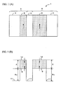
- Fig. 1 shows the configuration of a spin-filter transistor according to the present example
- Fig. 1 (A) shows a schematic cross section.
- Fig. 1 (B) shows an energy band of the conduction band (or the valence band) of the configuration shown in Fig. 1 (A) , also showing the spin direction of the spin band in the barrier layer.
- the carriers are holes, the direction of magnetization at the band edge corresponds to the spin direction; when the carriers are electrons, the relative magnetization configuration is opposite to that of the spin direction of the band edge.
- a spin-filter transistor 1 comprises a spin injector 5 comprising: a first ferromagnetic barrier layer 2; a first nonmagnetic electrode layer 3 joined to one end surface of the first ferromagnetic barrier layer 2; and a second nonmagnetic electrode layer 4 joined to the other end surface of the first ferromagnetic barrier layer 2.
- the spin-filter transistor 1 also comprises a spin analyzer 8 comprising: a second ferromagnetic barrier layer 6; a second nonmagnetic electrode layer 4 joined to one end surface of the second ferromagnetic barrier layer 6; and a third nonmagnetic electrode layer 7 joined to the other end surface of the second ferromagnetic barrier layer 6.
- the spin injector 5 and the spin analyzer 8 shares the second nonmagnetic electrode layer 4.
- the first, second, and third nonmagnetic electrode layers 3, 4, and 7 may be formed by a nonmagnetic metal, an n-type nonmagnetic semiconductor, or a p-type nonmagnetic semiconductor.
- the thickness of the second nonmagnetic electrode layer 4 is preferably not greater than the mean free path within the nonmagnetic electrode layer 4 of the spin-polarized hot carriers injected from the spin injector. By making the base width shorter than the mean free path, the current transfer ratio can be made 0.5 or greater, so that current amplification can be achieved.
- the first and second ferromagnetic barrier layers 2 and 6 may comprise an insulating ferromagnetic semiconductor or a ferromagnetic insulator.
- the energy band of the ferromagnetic barrier layer is spin-split by magnetic exchange interaction, such that an energy region is created at the band edge where only an up spin or a down spin exists.
- Such a spin-polarized band is referred to as a spin band, and this energy region band is referred to as a spin-split width ⁇ .
- the solid lines with an arrow ⁇ on the ferromagnetic barrier layers 2 and 6 indicate the edge of the band where an up spin can exist, namely, an up-spin band edge 9.
- the solid lines with an arrow ⁇ indicate the edge of the band where a down spin can exist, namely, a down-spin band edge 10.
- the region between the up-spin band edge 9 and the down-spin band edge 10 in Fig. 1 (B) is a region where only an up spin can exist.
- a region with a higher energy than that of the down-spin band edge 10 is a region where both up spin and down spin can exist.
- Fig. 1 (B) shows a case where the spin band of up spin is lower than the spin band of down spin, the opposite state is also possible.
- the first ferromagnetic barrier layer 2 has a thickness such that the carriers can be transmitted from the first nonmagnetic electrode layer 3 to the second nonmagnetic electrode layer 4 by tunneling, such as Fowler-Nordheim tunneling (to be hereafter referred to as "FN tunneling") or a direct tunneling, in response to the application of a voltage to the first nonmagnetic electrode layer 3 and to the second nonmagnetic electrode layer 4.
- tunneling such as Fowler-Nordheim tunneling (to be hereafter referred to as "FN tunneling") or a direct tunneling, in response to the application of a voltage to the first nonmagnetic electrode layer 3 and to the second nonmagnetic electrode layer 4.
- FN tunneling Fowler-Nordheim tunneling
- a direct tunneling refers to the phenomenon in which the carriers directly pass through a thin potential barrier.
- the FN tunneling refers to the phenomenon in which the tunneling current due to a direct tunneling can be ignored up to a certain applied voltage and in which the carriers tunnel through the triangular potential at the top of a potential barrier produced by the application of a voltage exceeding a certain value.
- the voltage applied to the first nonmagnetic electrode layer 3 and the second nonmagnetic electrode layer 4 may be in the voltage range used in the conventional memory circuit, such as on the order of several hundred mV to several volts.
- the second ferromagnetic barrier layer 6 needs to be sufficiently thick that there is no thermionic emission of the carriers or a current due to tunneling (the so-called leak current) from the second nonmagnetic electrode layer 4 to the third nonmagnetic electrode layer 7.
- the nonmagnetic electrode layers 3, 4, 7 and the ferromagnetic electrode layers 2 and 6 form the energy band structure shown in Fig. 1 (B) .
- Solid lines 11 in the nonmagnetic electrode layer Fig. 1 (B) indicate the Fermi energy of the metal, the Fermi energy of an n-type (p-type) semiconductor, or the energy at the bottom of the conduction band (at the top of the valence band).
- the lower energy barrier in the ferromagnetic barrier layers 2 and 6 corresponding to the solid lines 11 at the nonmagnetic electrode layer is indicated by ⁇ C
- the spin-split width is indicated by ⁇ .
- the ferromagnetic barrier layers 2 and 6 may have different values of ⁇ C and ⁇ , the following description concerns a case where the ferromagnetic barrier layers 2 and 6 have the same values of ⁇ C and ⁇ .
- a nonmagnetic metal or an n-type semiconductor is used for the nonmagnetic electrode layers 3, 4, and 7, and an insulating ferromagnetic semiconductor or a ferromagnetic insulator is used for the ferromagnetic barrier layers 2 and 6.
- the up-spin band edge 9 and the down-spin band edge 10 are produced by the spin splitting of the bottom of the conduction band of the ferromagnetic barrier layers 2 and 6.
- a p-type semiconductor is used for the nonmagnetic electrode layer 3, 4, 7, and an insulating ferromagnetic semiconductor or a ferromagnetic insulator is used for the ferromagnetic barrier layers 2 and 6.
- the up-spin band edge 9 and the down-spin band edge 10 of the ferromagnetic barrier layer 2 and 6 are produced by the spin splitting of the top of the valence band.
- the operating principle of the above-described spin-filter transistor is described in detail.
- the notational system for the hot electron transistor will also be used for simplicity's sake.
- the first nonmagnetic electrode layer 3 and the first ferromagnetic barrier layer 2 will be referred to as an emitter 21
- the second nonmagnetic electrode layer 4 will be referred to as a base 22
- the second ferromagnetic barrier layer 6 and the third nonmagnetic electrode layer 7 will be referred to as a collector 23
- the first nonmagnetic electrode layer 3 will be referred to as an emitter electrode 3
- the third nonmagnetic electrode layer 7 will be referred to as a collector electrode 7.
- the following also concerns the case where the carriers are electrons as an example (the case where the carriers are holes will not be described because such a case is substantially the same in terms of operating principle).
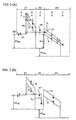
- Fig. 2 shows energy band diagrams in a case where a common-base bias voltage is applied between the emitter, base, and collector of the spin-filter transistor of the present example.
- Fig. 2 (A) shows a case where the magnetization configurations of the first and second ferromagnetic barrier layers are parallel to each other
- Fig. 2 (B) shows a case where the magnetization configurations of the first and second ferromagnetic barrier layers are antiparallel to each other, corresponding to Fig. 2 (A) .
- a bias voltage V EB is applied across emitter 21 and base 22, and a bias voltage V CB is applied across base 22 and collector 23.
- the magnitude of V EB is set such that the relationship ( ⁇ C ⁇ qV EB ⁇ ⁇ C + ⁇ ) is satisfied, where q is the elementary charge.
- the emitter 21 functions as a spin injector for injecting spin-polarized hot electrons to base 22.
- the emitter 21 functions as a spin injector for injecting spin-polarized hot electrons to base 22.
- the barrier height for the up-spin electrode 24 corresponds to the energy up to an up-spin band edge 9 of the first ferromagnetic barrier layer 2, or ⁇ C .
- the barrier height for the down-spin electrode 25 corresponds to the energy up to a down-spin band edge 10 of the first ferromagnetic barrier layer 2, or ⁇ C + ⁇ .
- the collector 23 of the spin-filter transistor functions as a spin analyzer for selecting the direction of the spin-polarized hot electrons injected into the base 22. Specifically, the spin-polarized electrons 26 that have been rendered into hot electrons by the bias voltage V EB and injected into the base 22 can arrive at the boundary between base 22 and collector 23 without losing energy, or "ballistically," because the width of base 22 is set to be not greater than the mean free path of the spin-polarized hot electrons 26. In the second ferromagnetic barrier layer 6 of collector 23, there is also produced two barriers with different barrier heights due to the spin splitting of the conduction band. As shown in Fig.
- the current transfer ratio of the current that flows from the emitter to the collector greatly differs depending on the relative magnetization configuration of the first ferromagnetic barrier layer 2 of emitter 22 and the second ferromagnetic barrier layer 6 of collector 23.
- the current gain of collector current due to base current greatly differs.
- Fig. 3 shows the static characteristics of the spin-filter transistor of the present example in a common-base configuration.
- the horizontal axis shows collector-base voltage V CB in the upper-right portion and emitter-base voltage V EB to the left.
- the vertical axis shows emitter current I E , the base current I B , and collector current I C .
- Fig. 3 (A) shows the static characteristics in a case where the magnetization configurations of the ferromagnetic barrier layers of the emitter and the collector are parallel.
- Fig. 3 (B) shows the static characteristics when the magnetization configurations are antiparallel. In both Fig.
- ⁇ indicates the current transfer ratio
- ⁇ indicates the current gain
- subscripts ⁇ and ⁇ indicate the parallel and antiparallel relative magnetization configuration, respectively, of the ferromagnetic barrier layers of the emitter and collector.
- Fig. 3 (A) when the magnetization configurations of the emitter and the collector are parallel, most of the emitter current I E can serve as the collector current I C .
- Fig. 3 (B) when the magnetization configurations are antiparallel, most of the emitter current I E can serve as the base current I B .
- the collector current I C can be controlled by the base current I B in the transistor of the present example.
- the current gain can be controlled by the relative magnetization configuration of the first and second ferromagnetic barrier layers.
- the ferromagnetic barrier layer of the spin-filter transistor of the present example may comprise a ferromagnetic semiconductor, such as EuS, EuSe, or EuO, for example. It may also comprise a ferromagnetic insulator, such as R 3 Fe 5 O 12 (where R is a rare-earth element).
- the nonmagnetic electrode layer may comprise any material as long as it is nonmagnetic. Examples include metals, such as Al and Au, and nonmagnetic semiconductors, such as Si and GaAS, that have been doped with a high concentration of impurity.
- the ferromagnetic barrier layer comprises EuS and the nonmagnetic electrode layer comprises AI
- the barrier height ⁇ C is 1.4eV and the spin-split width ⁇ is 0.36eV.
- the spin-filter transistor of the present embodiment can be produced by a known method, such as molecular beam epitaxy, vacuum evaporation, or sputtering, using the above-described materials.
- nonvolatile memory comprising a to be defined spin transistor of the present invention as a memory cell will be described.
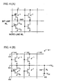
- Fig. 4 (A) shows an example of a memory cell employing a spin-filter transistor 1 of the present example.
- a number of spin-filter transistors are arranged in a matrix, with the emitter terminals E grounded and the collector terminals C and the base terminals B connected to a bitline BL for sensing and a wordline WL for sensing, respectively.
- a wordline for writing intersects a bitline for writing above the spin-filter transistors such that these lines are electrically insulated from other wires.
- the wordline for writing and the bitline for writing may be combined with the aforementioned bitline BL for sensing and wordline WL for sensing, as shown in Fig. 4 (A) .
- a memory cell can be formed by a single spin-filter transistor, and also a simple wiring arrangement can be adopted.
- the present memory cell arrangement makes it possible to easily configure a layout suitable for high-density integration.
- the example shown in Fig. 4 (B) also adopts a similar cell arrangement.
- a memory circuit according to the present embodiment will be described.
- a second nonmagnetic electrode 4 which is the base of the spin-filter transistor 1 ( Fig. 1 ) is connected to a wordline 42;
- a third nonmagnetic electrode 7, which is the collector electrode of the spin-filter transistor 1 is connected to a bitline 43;
- the bitline 43 is connected to a power supply (V CC ) 45 via a load (R L ) 44;
- a pure resistance is used as the load in the illustrated example, an active load consisting of a transistor may be used.
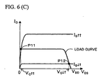
- a specific wordline 42 is selected and a bias is applied across the emitter-base junction, and a power supply voltage V CC from the power supply 45 is applied to the bitline 43 via the load resistance 44. Then, the stored information is sensed using the magnitude of an output voltage Vo that appears at the bitline 43.
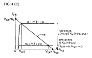
- the vertical axis of Fig. 4 (C) shows collector current I C .
- the horizontal axis shows collector-emitter voltage V CE .
- the graph thus shows the I C -V CE characteristics of the spin-filter transistor and a load line 46 of the load resistance 44 in the same chart.
- the output voltage V o is determined by the intersection of these characteristics. Specifically, the output signals in the cases where the magnetization configuration between the first and second ferromagnetic barrier layers 2 and 6 is parallel and antiparallel would be V o ⁇ and V o ⁇ , as shown in Fig. 4 (C) .
- the absolute values of V o ⁇ and V o ⁇ and the ratio of V o ⁇ and V o ⁇ can be optimized by means of circuit parameters (R L and V CC ).
- circuit parameters R L and V CC
- the spin-filter effect utilized by the transistor of the present example is provided by the spin band splitting of the ferromagnet, such that a higher spin selectivity can be obtained than is possible with the TMR effect of MTJ.
- the current transfer ratio ⁇ (defined as being equal to I C /I E ) can be 0.5 or more when the relative magnetization configuration between the first and second ferromagnetic barrier layers is parallel.
- the relative magnetization configuration is antiparallel, the current transfer ratio is extremely small.
- the change in the current transfer ratio between parallel magnetization and antiparallel magnetization is even more amplified in terms of current gain ⁇ (defined as being equal to I E /I B ).
- spin transistor nonvolatile memory circuit utilizing a transistor (to be hereafter referred to as a "spin transistor") with output characteristics that depend on the spin direction of the carriers is described.
- the memory circuit of the present invention relates to a nonvolatile memory circuit utilizing a spin transistor.
- a spin transistor includes a ferromagnet such as a ferromagnetic metal or a ferromagnetic semiconductor. The output characteristics are changed by controlling the spin direction of the carriers depending on the magnetization configuration of the ferromagnet. Information is stored in terms of the magnetization configuration of the ferromagnet inside the spin transistor, and the stored information is sensed using the output characteristics of the transistor that reflect the magnetization configuration inside the spin transistor.
- a 1-bit nonvolatile memory cell can be configured with a single spin transistor. Furthermore, the value of the output signal corresponding to the stored information can be optimized by peripheral circuitry connected to the memory cell.
- the spin transistor comprises at least one each of a ferromagnet layer (free layer) capable of independently controlling the relative magnetization configuration using a magnetic field or the like, and a ferromagnet layer (pin layer) with a fixed relative magnetization configuration or having a larger coercivity than that of the free layer.
- the output characteristics of the transistor can be controlled by the relative magnetization configuration of the free layer and the pin layer even under the same bias condition.
- the relative magnetization configuration of the free layer and the pin layer can be rendered into two configurations, namely, parallel or antiparallel. These two magnetization configurations are associated with binary stored information.
- the spin transistor based on a conduction phenomenon that varies depending on the spin direction of the carrier, such as spin-dependent scattering, tunneling magnetoresistance effect, or spin-filter effect, output characteristics corresponding to the internal magnetization configuration of the transistor can be obtained.
- the spin transistor comprises a first electrode structure for injecting spin-polarized carriers, a second electrode structure for receiving the spin-polarized carriers, and a third electrode structure for controlling the quantity of spin-polarized carriers that are transported from the first electrode structure to the second electrode structure.
- the spin transistors operate on the same principle as that of the conventional transistors with the exception of the involvement of the spin-dependent conduction phenomenon.
- the spin transistors can be classified into current-driven transistors such as bipolar transistors, and voltage-driven transistors such as field-effect transistors.
- the first electrode structure corresponds to the emitter
- the second electrode structure corresponds to the collector
- the third electrode structure corresponds to the base.
- the spin-filter transistor described with reference to the present example is a current-driven transistor.
- the first electrode structure corresponds to the source
- the second electrode structure corresponds to the drain
- the third electrode structure corresponds to the gate.
- the output current in the spin transistor (collector current or drain current) changes depending on the magnetization configuration of the ferromagnet contained in the spin transistor even under the same bias condition.
- the spin transistor The details of the spin transistor will be described later.
- the general output characteristics of a spin transistor and a nonvolatile memory employing a spin transistor will be described. It is assumed in the following that the relative magnetization configuration between the free layer and the pin layer can be rendered parallel or antiparallel by applying a magnetic field to the free layer in the spin transistor. It is also assumed that the magnetization configuration can exist stably unless a magnetic field exceeding the coercivity of the free layer is applied.
- Fig. 5 (A) schematically shows an example of the output characteristics of a current-driven spin transistor.
- the collector current I C can be controlled by the magnitude of the base current I B , it is also dependent on the magnetization configuration of the ferromagnet contained in the spin transistor.
- the collector current I C ⁇ in the case of parallel magnetization is large, whereas the collector current I C ⁇ in the case of antiparallel magnetization is small.
- Fig. 5 (B) schematically shows an example of the output characteristics of a voltage-driven spin transistor.
- a conventional field-effect transistor such as a MOS transistor
- V GS gate source voltage
- V T threshold value
- the spin transistor when the gate source voltage (V GS ) is smaller than the threshold value V T (V GS ⁇ V T ), the spin transistor is in an off state where hardly any drain current flows.
- the drain current I D ⁇ is larger for parallel magnetization whereas the drain current I D ⁇ is small for antiparallel magnetization.
- the spin transistor whether it is current-driven or voltage-driven, can electrically detect the magnitude of the relative magnetization configuration of the free layer and the pin layer contained in the device using the magnitude of the collector current or the drain current.
- the relative magnetization configuration in the ferromagnet can exist stably unless a magnetic field exceeding the coercivity of the free layer is externally applied.
- the spin transistor can store binary information in a nonvolatile manner by rendering the relative magnetization configuration of the free layer and the pin layer contained in the device parallel or antiparallel. Therefore, using the spin transistor, a 1-bit nonvolatile memory cell can be configured with a single spin transistor.
- nonvolatile memory employing a voltage-driven spin transistor will be described.
- the same configuration can be adopted where a current-driven type spin transistor is used in a memory cell.
- Fig. 6 (A) shows an example of the memory cell using the spin transistor.
- Fig. 6 (B) shows an example of a memory circuit configured with the memory cell. The relationship between Fig. 6 (A) and Fig. 6 (B) is the same as that between Fig. 4 (A) and Fig. 4 (B) .
- a number of spin transistors 150 are arranged in a matrix, with the sources S grounded and the drains D and the gates G connected to a bitline BL for sensing and a wordline WL for sensing, respectively.
- a wordline for writing and a bitline for writing are arranged to intersect one another above the spin transistors 150 in a manner electrically insulated from other wires.
- the wordline for writing and the bitline for writing may be combined with the aforementioned bitline BL for sensing and the wordline WL for sensing, as shown in Fig. 6 (A) and (B) .
- a memory cell can be configured with a single spin transistor, and also a very simple wiring arrangement can be adopted.
- a layout suitable for microfabrication can be easily obtained by, for example, causing adjacent memory cells to use the source in common.
- bitline BL bitline BL
- wordline WL wordline
- Information can be written over by causing a current to flow through the bitline BL and the wordline WL that intersect over a selected memory cell and then inverting the free layer of the selected memory cell with a composed magnetic field induced by the current through the respective lines.
- a current value that is caused to flow in each line is set in advance such that no magnetization inversion is caused by a magnetic field emitted by one of the lines.
- a voltage is applied to the wordline WL of a selected cell so as to cause the spin transistor to conduct, and then a voltage is applied to the bitline BL to detect the magnitude of the drain current. Based on the magnitude of the drain current, the relative magnetization configuration of the free layer and the pin layer can be detected.
- Fig. 6 (B) shows the memory circuit shown in Fig. 6 (A) , to a bitline end of which an output terminal V o is connected, with a branch from the output terminal V o connected to a power supply voltage V DD via a load.
- Fig. 6 (C) shows the static characteristics and operating points of the memory cell shown in Fig. 6 (B) .
- an active load 160 consisting of a depletion-type MOS transistor is used as the load in this example, pure resistance may be used, as shown in Fig. 4 (B) . Referring to Fig.
- a gate voltage V GS is applied to the gate of a spin transistor 150 and a power supply voltage V DD is applied to the bitline BL via a load.
- V DD power supply voltage
- the output signal V o would be V o ⁇ or V o ⁇ for the parallel or antiparallel magnetization, respectively.
- the absolute values of the output signals and their ratio (V o ⁇ /V o ⁇ ) can be optimized using the transistor characteristics of the active load or the parameters of peripheral circuitry, such as V DD .
- the memory circuit of the present embodiment is advantageous in that output signals of a desired magnitude can be easily obtained and in that a high-speed sensing can be performed.
- a spin transistor that can be used in the nonvolatile memory circuit of the present embodiment will be described with reference to the drawings, using abbreviations FM for ferromagnetic metal, FS for electrically conductive ferromagnetic semiconductor, IFS for insulating ferromagnetic semiconductor, and NM for a nonmagnetic material.
- FM ferromagnetic metal
- FS electrically conductive ferromagnetic semiconductor
- IFS insulating ferromagnetic semiconductor
- NM for a nonmagnetic material.
- an "NM metal” designates a nonmagnetic metal
- an "NM semiconductor” designates a nonmagnetic semiconductor.
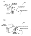
- Fig. 7 shows an energy band diagram of a hot-electron transistor type spin transistor.
- a spin transistor 200 comprises an emitter 201 and a base 205 that are formed by FM or FS.
- the spin transistor 200 comprises emitter 201 formed by FM (or FS); emitter barrier 203 formed by NM; base 205 formed by FM (or FS); collector barrier 207 formed by NM; and collector 211 formed by NM.
- NM may be either a nonmagnetic metal or a nonmagnetic semiconductor.
- spin-polarized hot carriers are tunnel-injected from the emitter 201 to the base 205 via the emitter barrier 203.
- the injected spin-polarized hot carriers hardly experience spin-dependent scattering within the base 205.
- the base width such that the carriers can pass through the base 205 ballistically, the carriers can be transported beyond the collector barrier 207 to the collector 211. This is a transistor operation similar to that of a conventional hot electron transistor.
- the spin-polarized hot carriers injected from the emitter 201 to the base 205 lose energy due to the spin-dependent scattering within the base 205 and are therefore unable to overcome the collector barrier 207, resulting in a base current.
- the current transfer ratio drops as compared with the case of parallel magnetization. Therefore, even if the same bias is applied to the spin transistor 200, the current transfer ratio or current gain varies depending on the difference in the relative magnetization configuration between the emitter 201 and the base 205.
- the spin transistor 200 can be operated at room temperature by appropriately selecting the collector barrier height, for example.
- the base width In the spin transistor 200, if the ratio of the current transfer ratio in the case where the emitter-base junction has parallel magnetization and that in the case where the junction has antiparallel magnetization is to be increased, the base width must be sufficiently large so that the spin-dependent scattering can effectively function. However, when the base width is increased, the current transfer ratio becomes smaller even when the emitter-base junction has parallel magnetization, dropping below 0.5, for example. Thus, there is a tradeoff between an increase in the base width and a decrease in amplification function.
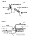
- Fig. 8 shows an energy band diagram of a hot-electron transistor type spin transistor in which thermionic emission is utilized as a mechanism for injecting spin polarized carriers to the base.
- a spin transistor 220 comprises an emitter 221 formed by FM (or FS); a base 225 formed by FM (or FS); and an emitter barrier 223 disposed between the emitter and the base and formed by NM.
- a collector barrier 227 formed by NM and a collector 231 formed by NM.
- the emitter barrier 223 and collector barrier 227 may be formed by a nonmagnetic semiconductor.
- the collector 231 may be formed by a nonmagnetic semiconductor or a nonmagnetic metal.
- an ohmic contact or a tunnel contact is formed between the emitter 221 and the emitter barrier 223, an ohmic contact or a tunnel contact is formed.
- a junction exhibiting a band discontinuity as shown in Fig. 9 is formed between the base 225 and the emitter barrier 223, and between the base 225 and the collector barrier 227.
- This band discontinuity can be realized by a Schottky junction between NM semiconductor and FM, or by a heterojunction between NM semiconductor and FS.
- a Schottky junction may be formed between FS and FM, and the resultant Schottky barrier may be used as the emitter barrier, with FS and FM functioning as emitter and base, respectively.
- the spin-polarized carriers diffused from the emitter 221 to the emitter barrier 223 through the application of a bias to the base 225 with respect to the emitter 221 are injected to the base 225 as hot carriers by thermionic emission.
- the spin-polarized hot carriers injected into the base 225 can reach the collector without being subjected to spin-dependent scattering.
- the spin-polarized hot carriers are rendered into a base current by spin-dependent scattering.
- the transistor 220 because it utilizes spin-dependent scattering in the base, there is a tradeoff, as in the above-described spin transistor 200, between the ratio of the current transfer ratio in the case of parallel magnetization and that in the case of antiparallel magnetization, and the current transfer ratio in the case of parallel magnetization.
- the transistor 220 is advantageous as compared with the spin transistor 200, which utilizes tunnel injection, in that a larger current driving force can be obtained and in that a room temperature operation can be easily realized.
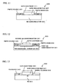
- FIG. 9 shows an energy band diagram of a hot-electron transistor type spin transistor utilizing the spin-filter effect.
- a spin transistor 240 shown in Fig. 9 comprises an emitter barrier 243 and a collector barrier 247 that are formed by IFS. Via an emitter 241, which is formed by an NM semiconductor (or an NM metal), the carriers with one spin can be selectively injected into the base 245, which is formed by an NM semiconductor (or an NM metal), through the spin-filter effect provided by the emitter barrier 243.
- the spin-polarized hot carriers injected into the base 245 are transported to the base 245 ballistically.
- the spin transistor 240 is biased such that the spin-polarized hot carriers are injected into the energy-split width between an up-spin band (a spin band edge designated by the upward arrow in Fig. 9 ) and a down-spin band (a spin band edge designated by the downward arrow in Fig. 9 ).
- the spin-polarized hot carriers injected into the base 245 can overcome the barrier of the spin band of lower energy in the collector barrier 247 through the spin-filter effect of the collector barrier 247, and therefore propagate to a collector 251, which is formed by an NM semiconductor (or an NM metal).
- a collector 251 which is formed by an NM semiconductor (or an NM metal).
- the emitter barrier 243 and the collector barrier 247 have antiparallel magnetization, most of the spin-polarized hot carriers cannot overcome the collector barrier 247 because of the spin-filter effect of the collector barrier 247, resulting in a base current.
- the current transfer ratio (or the current gain) differs depending on the relative magnetization configuration of the emitter barrier 243 and the collector barrier 247. Because the spin-filter effect provides a very high spin-selectivity, the ratio of current transfer ratio in the case of parallel magnetization and that in the case of antiparallel magnetization can be increased.
- the base width can be made sufficiently small. Therefore, in contrast to the spin transistor that utilizes spin-dependent scattering, as in the cases shown in Figs. 7 and 8 , the spin transistor 240 is advantageous in that there is no tradeoff between the current gain relating to the base width and the spin selectivity.
- Fig. 10 shows an energy band diagram of a tunnel base transistor type spin transistor.
- a tunnel base transistor type spin transistor 260 comprises an emitter 261 and a collector 265 that are formed by a p-type (or an n-type) FS, and a tunnel base 263, which is formed by an n-type (or a p-type) NM semiconductor.
- a heterojunction of type II is preferably used so that the base 263 becomes a barrier to the holes (or electrons). The base width is reduced sufficiently that a tunneling current from the emitter to the collector is produced.
- the emitter 261 and the collector 265 have parallel magnetization, the carriers with the majority spin in the emitter can be easily transported to the collector 265 through tunneling, namely, the tunnel conductance is large.
- the tunnel conductance is reduced by the tunneling magnetoresistance (TMR) effect.
- TMR tunneling magnetoresistance
- the change in collector current that depends on the magnetization configuration between emitter and collector can be increased.
- the TMR effect in the base cannot be expected.
- the carriers injected into the collector are subjected to spin-dependent scattering in the collector resistance, resulting in increased resistance.
- the magnitude of the collector current can be varied by the magnetization configuration in the emitter-collector junction. It is possible, however, that the effect is not so large as that obtained with the TMR effect because the resistance change through spin-dependent scattering is small.
- Fig. 11 shows a cross-section of a MOS transistor type spin transistor.
- the MOS transistor type spin transistor 300 comprises an NM semiconductor 301 on which a source 303 formed by FM, a drain 305 formed by FM, and a gate electrode 311 are formed, the gate electrode via a gate insulating film 307.
- a Schottky junction of FM and an NM semiconductor is used for the source 303 and the drain 305.
- the other structures are the same as those of a conventional MOS transistor.
- the mutual conductance differs depending on the relative magnetization configuration between the source and drain.
- the source 303 and the drain 305 may be formed by FS, and a pn junction is formed between each and the semiconductor 301.
- Fig. 12 shows a cross section of a modulation-doped transistor type spin transistor.
- the spin transistor 320 comprises a source 323 of FM (or FS) in contact with the two-dimensional carriers gas produced at the boundary between a first NM semiconductor 321 and a second NM semiconductor 327; a drain 325 formed by FM (or FS); and a gate electrode 331.
- the spin transistor 320 is identical to a conventional modulation-doped transistor with the exception that the source 323 and drain 325 are formed by a ferromagnet.
- Spin-polarized carriers are injected from the source 323 to a channel 333 formed by the two-dimensional carrier gas.
- the spin-polarized carriers that reach the drain 325 have different mutual conductance depending on the relative magnetization configuration of the source 323 and the drain 325 due to spin-dependent scattering in the drain 325.
- Fig. 13 shows a cross section of a MOS transistor type spin transistor in which the channel region is formed by FS.
- the spin transistor 340 shown in Fig. 13 comprises FS 341 on which a source 343 formed by FM, a drain 345 formed by NM (or FM or FS), and a gate electrode 351 via a gate insulating film 347 are formed.
- a Schottky junction of FM and FS is used in the source 343; except for that, the structure is identical to that of a conventional MOS transistor.
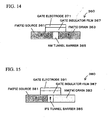
- Fig. 14 shows a cross section of a spin transistor 360 according to the invention comprising a tunnel junction structure in which an insulating NM tunnel barrier 365 is disposed between a source 361 formed by FM (or FS) and a drain 363 formed by FM (or FS). It is a spin transistor with the gate electrode 371 disposed such that an electric field can be applied to the tunnel barrier 365.
- the thickness of the tunnel barrier 365 is preferably set such that no Fowler-Nordheim (FN) tunneling occurs when only a source-drain bias is applied.
- FN Fowler-Nordheim
- a triangular potential at the band edge of the tunnel barrier produced by applying a bias across the source-drain junction is varied by the gate voltage in order to induce FN tunneling and obtain a drain current.
- Fig. 15 shows a cross section of a spin transistor 380 according to the invention which is similar to the spin transistor 360 shown in Fig. 14 with the exception that the tunnel barrier comprises a tunnel barrier 385 formed by IFS. While a source 381 must be FM or FS, a drain 383 may not be a ferromagnet. In the IFS tunnel barrier layer 385, the barrier height differs depending on the spin direction of the carriers. A bias is therefore applied between the source and drain and across the source-gate junction such that the transistor conducts when the source 381 and the tunnel barrier 385 have parallel magnetization. Under the same bias condition, when the source 381 and tunnel barrier 385 have antiparallel magnetization, the tunnel barrier height as seen from the majority spin in the source 381 increases.
- the tunneling probability of the spin-polarized carriers decreases, leading to a decrease in drain current.
- the spin selectivity provided by this spin-filter effect is extremely large, the change in mutual conductance depending on the relative magnetization configuration of the source and drain can be increased by using a ferromagnet with a large spin polarization in the source 381.
- any of the above-described various spin transistors may be used as the memory cells for the memory circuit shown in Fig. 4 or Fig. 6 .
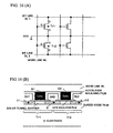
- Fig. 16 (A) shows an example of a memory cell of a common-source configuration.
- Fig. 16 (B) shows a cross section of the memory cell of a common-source configuration.
- the memory cell structure shown in Figs. 16 (A) and (B) comprises a first spin transistor Tr1 and a second spin transistor Tr2 that are disposed adjacent to one another; a wordline WL connecting a gate electrode G1 of the first spin transistor Tr1 and a gate electrode G2 of the second spin transistor Tr2; a first bitline BL1 connected to a first drain D1 of the first spin transistor Tr1; a second bitline BL2 connected to a second drain D2 of the second spin transistor; a ferromagnetic source S common to the first and second spin transistors Tr1 and Tr2; and a line connecting the common source to ground.
- the common source makes the cell structure suitable for higher-density integration.
- the voltage-driven spin transistors shown in Figs. 11 , 14, and 15 preferably comprise a highly insulating substrate, such as an SOI substrate as shown in Fig. 16 (B) , so as to reduce leakage current when the transistor is off.
- the two spin transistors according to the embodiments from Figures 14 and 15 of the present embodiment are characterized in that the output characteristics can be controlled by the relative magnetization configuration of the pin layer and free layer within the device.
- the relative magnetization configuration is nonvolatile, namely, the device does not require the feeding of power for retaining the magnetization configuration.
- the device can store binary information in terms of the relative magnetization configuration in a nonvolatile fashion.
- the relative magnetization configuration can be electrically detected.
- a 1-bit nonvolatile memory cell can be configured with a single spin transistor.
- a nonvolatile memory circuit comprising a spin transistor according to the two embodiments of the invention, the ratio of output signals as well as their magnitudes with respect to the stored information can be freely designed.
- the operating speed and the level of integration of a nonvolatile memory circuit can be increased.
- the output characteristics can be greatly changed by the relative magnetization configuration of the ferromagnetic barrier layers.
- a nonvolatile memory circuit comprising a memory cell employing this spin transistor with equivalent characteristics can store binary information in terms of the relative magnetization configuration of ferromagnets contained in the transistor.
- the relative magnetization configuration can also be detected electrically.
- the output signals with respect to the stored information can be freely designed.
- a high-speed and high integration-density nonvolatile memory circuit can be realized that comprises a 1-bit nonvolatile memory cell made up of a single transistor.
Abstract
Claims (8)
- Transistor à spin (360) comprenant une structure de jonction tunnel et une électrode de grille (371), dans lequel :ladite structure de jonction tunnel comprend :une barrière de tunnel (365) formée par un matériau non magnétique isolant (365) et qui est une barrière de tunnel simple ;une source (361) formée par un matériau ferromagnétique ;un drain (363) formé par un matériau ferromagnétique, ladite barrière de tunnel (365) étant placée entre ladite source (361) et ledit drain (363) de telle manière que la source (361) est liée à une surface d'extrémité de ladite barrière de tunnel (365) et le drain (363) est lié à l'autre surface d'extrémité de ladite barrière de tunnel (365) ; etune couche isolante de grille (367) placée entre ladite barrière de tunnel (365) et ladite électrode de grille (371).
- Transistor à spin (360) selon la revendication 1, dans lequel le matériau ferromagnétique utilisé dans ladite source (361) et ledit drain (363) est un métal ferromagnétique ou un semiconducteur ferromagnétique.
- Transistor à spin (360) selon la revendication 1, dans lequel l'épaisseur de ladite barrière de tunnel (365) est choisie de telle manière qu'un courant de tunnel peut circuler de ladite source (361) vers ledit drain (363) avec l'application d'une tension à ladite électrode de grille (371).
- Transistor à spin (360) selon la revendication 1, dans lequel l'amplitude de la conductance mutuelle ou du courant de sortie peut être commandée par les directions de magnétisation relatives de ladite source (361) et dudit drain (363).
- Transistor à spin (380) comprenant :une structure de jonction tunnel et une électrode de grille (391), dans lequel :ladite structure de jonction tunnel comprend :une barrière de tunnel (385) formée par un semiconducteur ferromagnétique isolant et qui est une barrière de tunnel simple ;une source (381) formée par un matériau ferromagnétique ;un drain (383) formé par un matériau non magnétique ou un matériau ferromagnétique, ladite barrière de tunnel (385) étant placée entre ladite source (381) et ledit drain (383) de telle manière que la source (381) est liée à une surface d'extrémité de ladite barrière de tunnel (385) et le drain (383) est lié à l'autre surface d'extrémité de ladite barrière de tunnel (385) ; etune couche isolante de grille (387) placée entre ladite barrière de tunnel (385) et ladite électrode de grille (391).
- Transistor à spin (380) selon la revendication 5, dans lequel le matériau ferromagnétique utilisé dans ladite source (381) est un métal ferromagnétique ou un semiconducteur ferromagnétique, dans ledit drain un métal ferromagnétique.
- Transistor à spin (380) selon la revendication 5, dans lequel l'épaisseur de ladite barrière de tunnel (385) est choisie de telle manière qu'un courant de tunnel peut circuler de ladite source (381) vers ledit drain (383) avec l'application d'une tension à ladite électrode de grille (391).
- Transistor à spin (380) selon la revendication 5, dans lequel l'amplitude de la conductance mutuelle ou du courant de sortie peut être commandée par les directions de magnétisation relatives de ladite source (381) et de ladite barrière de tunnel (385).
Applications Claiming Priority (5)
| Application Number | Priority Date | Filing Date | Title |
|---|---|---|---|
| JP2002217336 | 2002-07-25 | ||
| JP2002217336 | 2002-07-25 | ||
| JP2003086145A JP4477305B2 (ja) | 2002-07-25 | 2003-03-26 | スピントランジスタ及びそれを用いた不揮発性メモリ |
| JP2003086145 | 2003-03-26 | ||
| PCT/JP2003/009438 WO2004012272A1 (fr) | 2002-07-25 | 2003-07-25 | Transistor a spin utilisant un effet de filtre a spin et memoire non volatile utilisant un transistor a spin |
Publications (3)
| Publication Number | Publication Date |
|---|---|
| EP1555694A1 EP1555694A1 (fr) | 2005-07-20 |
| EP1555694A4 EP1555694A4 (fr) | 2008-06-04 |
| EP1555694B1 true EP1555694B1 (fr) | 2012-02-29 |
Family
ID=31190300
Family Applications (1)
| Application Number | Title | Priority Date | Filing Date |
|---|---|---|---|
| EP03771333A Expired - Fee Related EP1555694B1 (fr) | 2002-07-25 | 2003-07-25 | Transistor a spin utilisant un effet de filtre a spin et memoire non volatile utilisant un transistor a spin |
Country Status (8)
| Country | Link |
|---|---|
| US (4) | US7423327B2 (fr) |
| EP (1) | EP1555694B1 (fr) |
| JP (1) | JP4477305B2 (fr) |
| KR (1) | KR100977829B1 (fr) |
| CN (1) | CN100470844C (fr) |
| AU (1) | AU2003252691A1 (fr) |
| TW (1) | TWI310184B (fr) |
| WO (1) | WO2004012272A1 (fr) |
Families Citing this family (33)
| Publication number | Priority date | Publication date | Assignee | Title |
|---|---|---|---|---|
| US7528428B2 (en) | 2003-03-07 | 2009-05-05 | Japan Science And Technology Agency | Field-effect transistor with spin-dependent transmission characteristics and non-volatile memory using the same |
| JP4212397B2 (ja) | 2003-03-28 | 2009-01-21 | 株式会社東芝 | 磁気メモリ及びその書き込み方法 |
| CN101159287B (zh) * | 2003-03-31 | 2010-06-09 | 独立行政法人科学技术振兴机构 | 具有自旋相关转移特性的隧道晶体管及使用了它的非易失性存储器 |
| US7045368B2 (en) * | 2004-05-19 | 2006-05-16 | Headway Technologies, Inc. | MRAM cell structure and method of fabrication |
| US7411235B2 (en) | 2004-06-16 | 2008-08-12 | Kabushiki Kaisha Toshiba | Spin transistor, programmable logic circuit, and magnetic memory |
| JP2006237304A (ja) * | 2005-02-25 | 2006-09-07 | Osaka Industrial Promotion Organization | 強磁性伝導体材料およびその製造方法、並びに磁気抵抗素子、電界効果トランジスタ |
| EP1705665B1 (fr) * | 2005-03-24 | 2008-04-02 | Hitachi Ltd. | dispositif du contrôle de la conduction |
| JP5030397B2 (ja) * | 2005-06-24 | 2012-09-19 | 日本電信電話株式会社 | スピントランジスタ |
| US7372674B2 (en) * | 2005-07-22 | 2008-05-13 | Hitachi Global Storage Technologies Netherlands B.V. | Magnetic tunnel transistor with high magnetocurrent and stronger pinning |
| US7646627B2 (en) | 2006-05-18 | 2010-01-12 | Renesas Technology Corp. | Magnetic random access memory having improved read disturb suppression and thermal disturbance resistance |
| JP4883982B2 (ja) | 2005-10-19 | 2012-02-22 | ルネサスエレクトロニクス株式会社 | 不揮発性記憶装置 |
| JP4693634B2 (ja) * | 2006-01-17 | 2011-06-01 | 株式会社東芝 | スピンfet |
| JP2008047706A (ja) | 2006-08-16 | 2008-02-28 | Nec Lcd Technologies Ltd | 半導体回路及びそれを用いた半導体装置 |
| JP4455558B2 (ja) * | 2006-09-08 | 2010-04-21 | 株式会社東芝 | スピンmosfet |
| JP5157268B2 (ja) * | 2007-06-13 | 2013-03-06 | 株式会社日立製作所 | スピン蓄積磁化反転型のメモリ素子及びスピンram |
| KR100862216B1 (ko) * | 2007-08-02 | 2008-10-09 | 한국과학기술원 | 커패시터리스 디램 특성과 저항변화물질에 의한 비휘발성메모리 특성을 갖는 비휘발성 디램 |
| JP2009064826A (ja) | 2007-09-04 | 2009-03-26 | Tdk Corp | スピントランジスタ及びその製造方法 |
| US7936028B2 (en) | 2007-11-09 | 2011-05-03 | Samsung Electronics Co., Ltd. | Spin field effect transistor using half metal and method of manufacturing the same |
| US20090141409A1 (en) * | 2007-12-03 | 2009-06-04 | Santos Tiffany S | Spin filter spintronic devices |
| US8659852B2 (en) * | 2008-04-21 | 2014-02-25 | Seagate Technology Llc | Write-once magentic junction memory array |
| US8158964B2 (en) | 2009-07-13 | 2012-04-17 | Seagate Technology Llc | Schottky diode switch and memory units containing the same |
| WO2011036770A1 (fr) | 2009-09-25 | 2011-03-31 | 株式会社 東芝 | Circuit à transistors de chute avec fonction de mémoire et circuit de boîtier de commutation comprenant le circuit à transistors de chute |
| FR2966636B1 (fr) | 2010-10-26 | 2012-12-14 | Centre Nat Rech Scient | Element magnetique inscriptible |
| JP5778945B2 (ja) * | 2011-02-24 | 2015-09-16 | 株式会社東芝 | 連想メモリ |
| JP5225419B2 (ja) | 2011-03-28 | 2013-07-03 | 株式会社東芝 | スピンmosfetを用いたメモリ回路、メモリ機能付きパストランジスタ回路、スイッチングボックス回路、スイッチングブロック回路、およびフィールドプログラマブルゲートアレイ |
| CN103890855B (zh) * | 2011-08-18 | 2016-09-21 | 康奈尔大学 | 自旋霍尔效应磁性设备、方法及应用 |
| JP5665711B2 (ja) * | 2011-09-26 | 2015-02-04 | 株式会社東芝 | スピントランジスタおよびメモリ |
| US9270277B2 (en) * | 2012-06-28 | 2016-02-23 | Northwestern University | Emitter-coupled spin-transistor logic |
| EP2919274B1 (fr) | 2012-11-08 | 2018-04-18 | Japan Science and Technology Agency | Élément de vanne de spin latéral |
| DE102013209278B4 (de) * | 2013-05-17 | 2016-02-18 | Helmholtz-Zentrum Dresden - Rossendorf E.V. | Magnetisierbare Halbleiter mit permanenter Magnetisierung und deren Verwendung |
| CN105161613A (zh) * | 2015-08-18 | 2015-12-16 | 北京航空航天大学 | 一种基于双势垒结构的磁存储器件 |
| US9941469B2 (en) | 2015-10-06 | 2018-04-10 | International Business Machines Corporation | Double spin filter tunnel junction |
| CN112924781B (zh) * | 2021-01-26 | 2023-01-20 | 青岛海尔电冰箱有限公司 | 冰箱的智能检测设备 |
Family Cites Families (24)
| Publication number | Priority date | Publication date | Assignee | Title |
|---|---|---|---|---|
| JP3253696B2 (ja) * | 1992-09-11 | 2002-02-04 | 株式会社東芝 | 磁気抵抗効果素子 |
| US5565695A (en) | 1995-04-21 | 1996-10-15 | Johnson; Mark B. | Magnetic spin transistor hybrid circuit element |
| US5654566A (en) * | 1995-04-21 | 1997-08-05 | Johnson; Mark B. | Magnetic spin injected field effect transistor and method of operation |
| US5652445A (en) * | 1995-04-21 | 1997-07-29 | Johnson; Mark B. | Hybrid hall effect device and method of operation |
| JP3217703B2 (ja) * | 1995-09-01 | 2001-10-15 | 株式会社東芝 | 磁性体デバイス及びそれを用いた磁気センサ |
| US5962905A (en) * | 1996-09-17 | 1999-10-05 | Kabushiki Kaisha Toshiba | Magnetoresistive element |
| JP3258241B2 (ja) | 1996-09-30 | 2002-02-18 | 株式会社東芝 | 単一電子制御磁気抵抗素子 |
| US6069820A (en) | 1998-02-20 | 2000-05-30 | Kabushiki Kaisha Toshiba | Spin dependent conduction device |
| JP3556457B2 (ja) | 1998-02-20 | 2004-08-18 | 株式会社東芝 | スピン依存伝導素子とそれを用いた電子部品および磁気部品 |
| US6169688B1 (en) * | 1998-03-23 | 2001-01-02 | Kabushiki Kaisha Toshiba | Magnetic storage device using unipole currents for selecting memory cells |
| US6381171B1 (en) * | 1999-05-19 | 2002-04-30 | Kabushiki Kaisha Toshiba | Magnetic element, magnetic read head, magnetic storage device, magnetic memory device |
| JP4076197B2 (ja) | 1999-05-19 | 2008-04-16 | 株式会社東芝 | 磁性素子、記憶装置、磁気再生ヘッド、3端子素子、及び磁気ディスク装置 |
| JP3477638B2 (ja) | 1999-07-09 | 2003-12-10 | 科学技術振興事業団 | 強磁性2重量子井戸トンネル磁気抵抗デバイス |
| US6297987B1 (en) * | 1999-09-30 | 2001-10-02 | The United States Of America As Represented By The Secretary Of The Navy | Magnetoresistive spin-injection diode |
| JP3284239B2 (ja) | 2000-03-07 | 2002-05-20 | 東北大学長 | スピン偏極伝導電子生成方法および半導体素子 |
| GB0006142D0 (en) | 2000-03-14 | 2000-05-03 | Isis Innovation | Spin transistor |
| US6403999B1 (en) * | 2000-05-23 | 2002-06-11 | Spinix Corporation | Detection of polarized spin transport in semiconductors |
| US6355953B1 (en) | 2000-06-19 | 2002-03-12 | Simon Fraser University | Spintronic devices and method for injecting spin polarized electrical currents into semiconductors |
| US20020064004A1 (en) * | 2000-08-09 | 2002-05-30 | Worledge Daniel C. | Magnetoresistive double spin filter tunnel junction |
| AU2002230791A1 (en) * | 2000-10-26 | 2002-05-06 | University Of Iowa Research Foundation | Unipolar spin diode and transistor and the applications of the same |
| JP2003007980A (ja) * | 2001-06-20 | 2003-01-10 | Sony Corp | 磁気特性の変調方法および磁気機能装置 |
| JP3621367B2 (ja) * | 2001-09-17 | 2005-02-16 | 株式会社東芝 | スピントランジスタ |
| JP3834616B2 (ja) | 2001-11-13 | 2006-10-18 | 国立大学法人東北大学 | スピンフィルタ |
| KR100492482B1 (ko) * | 2002-09-04 | 2005-06-03 | 한국과학기술연구원 | Pembe로 제조된 상온 자성반도체 및 그 소자 |
-
2003
- 2003-03-26 JP JP2003086145A patent/JP4477305B2/ja not_active Expired - Fee Related
- 2003-07-24 TW TW092120200A patent/TWI310184B/zh not_active IP Right Cessation
- 2003-07-25 US US10/522,241 patent/US7423327B2/en not_active Expired - Fee Related
- 2003-07-25 AU AU2003252691A patent/AU2003252691A1/en not_active Abandoned
- 2003-07-25 WO PCT/JP2003/009438 patent/WO2004012272A1/fr active Application Filing
- 2003-07-25 EP EP03771333A patent/EP1555694B1/fr not_active Expired - Fee Related
- 2003-07-25 CN CNB038224801A patent/CN100470844C/zh not_active Expired - Fee Related
- 2003-07-25 KR KR1020057001401A patent/KR100977829B1/ko not_active IP Right Cessation
-
2007
- 2007-10-31 US US11/979,220 patent/US7825485B2/en not_active Expired - Fee Related
- 2007-10-31 US US11/979,221 patent/US7671433B2/en not_active Expired - Fee Related
-
2010
- 2010-09-22 US US12/923,450 patent/US8026563B2/en not_active Expired - Fee Related
Also Published As
| Publication number | Publication date |
|---|---|
| US7423327B2 (en) | 2008-09-09 |
| EP1555694A4 (fr) | 2008-06-04 |
| JP2004111904A (ja) | 2004-04-08 |
| US7671433B2 (en) | 2010-03-02 |
| EP1555694A1 (fr) | 2005-07-20 |
| US20080061336A1 (en) | 2008-03-13 |
| US20080067501A1 (en) | 2008-03-20 |
| TWI310184B (en) | 2009-05-21 |
| JP4477305B2 (ja) | 2010-06-09 |
| US7825485B2 (en) | 2010-11-02 |
| WO2004012272A1 (fr) | 2004-02-05 |
| US8026563B2 (en) | 2011-09-27 |
| KR20050025996A (ko) | 2005-03-14 |
| CN1685526A (zh) | 2005-10-19 |
| KR100977829B1 (ko) | 2010-08-24 |
| CN100470844C (zh) | 2009-03-18 |
| US20060043443A1 (en) | 2006-03-02 |
| US20110031545A1 (en) | 2011-02-10 |
| TW200405339A (en) | 2004-04-01 |
| AU2003252691A1 (en) | 2004-02-16 |
Similar Documents
| Publication | Publication Date | Title |
|---|---|---|
| EP1555694B1 (fr) | Transistor a spin utilisant un effet de filtre a spin et memoire non volatile utilisant un transistor a spin | |
| JP5121793B2 (ja) | スピン依存伝達特性を有する電界効果トランジスタ及びそれを用いた不揮発性メモリ | |
| US7397071B2 (en) | Tunnel transistor having spin-dependent transfer characteristics and non-volatile memory using the same | |
| JP5064430B2 (ja) | スピントランジスタ及びそれを用いた不揮発性メモリ | |
| KR20100073870A (ko) | 플로팅 바디 효과를 이용한 자기저항 메모리셀, 이를 포함하는 메모리 소자 및 그 동작 방법 | |
| US6696737B2 (en) | Unipolar spin transistor and the applications of the same | |
| JP4415146B2 (ja) | 強磁性半導体を用いた電界効果トランジスタと及びこれを用いた不揮発性メモリ |
Legal Events
| Date | Code | Title | Description |
|---|---|---|---|
| PUAI | Public reference made under article 153(3) epc to a published international application that has entered the european phase |
Free format text: ORIGINAL CODE: 0009012 |
|
| 17P | Request for examination filed |
Effective date: 20050225 |
|
| AK | Designated contracting states |
Kind code of ref document: A1 Designated state(s): AT BE BG CH CY CZ DE DK EE ES FI FR GB GR HU IE IT LI LU MC NL PT RO SE SI SK TR |
|
| AX | Request for extension of the european patent |
Extension state: AL LT LV MK |
|
| DAX | Request for extension of the european patent (deleted) | ||
| RBV | Designated contracting states (corrected) |
Designated state(s): DE FR GB |
|
| RIN1 | Information on inventor provided before grant (corrected) |
Inventor name: TANAKA, MASAAKI Inventor name: SUGAHARA, SATOSHIC/O TOKYO INST. TECHNOLOGY |
|
| A4 | Supplementary search report drawn up and despatched |
Effective date: 20080508 |
|
| 17Q | First examination report despatched |
Effective date: 20100409 |
|
| RIC1 | Information provided on ipc code assigned before grant |
Ipc: H01L 43/08 20060101ALI20110615BHEP Ipc: H01L 27/105 20060101ALI20110615BHEP Ipc: H01L 29/66 20060101ALI20110615BHEP Ipc: G11C 11/16 20060101ALI20110615BHEP Ipc: G11C 11/15 20060101ALI20110615BHEP Ipc: H01L 29/82 20060101AFI20110615BHEP |
|
| GRAP | Despatch of communication of intention to grant a patent |
Free format text: ORIGINAL CODE: EPIDOSNIGR1 |
|
| RIN1 | Information on inventor provided before grant (corrected) |
Inventor name: SUGAHARA, SATOSHIC/O TOKYO INST. TECHNOLOGY Inventor name: TANAKA, MASAAKI |
|
| GRAS | Grant fee paid |
Free format text: ORIGINAL CODE: EPIDOSNIGR3 |
|
| GRAA | (expected) grant |
Free format text: ORIGINAL CODE: 0009210 |
|
| AK | Designated contracting states |
Kind code of ref document: B1 Designated state(s): DE FR GB |
|
| REG | Reference to a national code |
Ref country code: GB Ref legal event code: FG4D |
|
| REG | Reference to a national code |
Ref country code: DE Ref legal event code: R096 Ref document number: 60340145 Country of ref document: DE Effective date: 20120426 |
|
| PLBE | No opposition filed within time limit |
Free format text: ORIGINAL CODE: 0009261 |
|
| STAA | Information on the status of an ep patent application or granted ep patent |
Free format text: STATUS: NO OPPOSITION FILED WITHIN TIME LIMIT |
|
| 26N | No opposition filed |
Effective date: 20121130 |
|
| REG | Reference to a national code |
Ref country code: DE Ref legal event code: R097 Ref document number: 60340145 Country of ref document: DE Effective date: 20121130 |
|
| REG | Reference to a national code |
Ref country code: FR Ref legal event code: PLFP Year of fee payment: 14 |
|
| REG | Reference to a national code |
Ref country code: FR Ref legal event code: PLFP Year of fee payment: 15 |
|
| PGFP | Annual fee paid to national office [announced via postgrant information from national office to epo] |
Ref country code: GB Payment date: 20170719 Year of fee payment: 15 Ref country code: FR Payment date: 20170724 Year of fee payment: 15 Ref country code: DE Payment date: 20170724 Year of fee payment: 15 |
|
| REG | Reference to a national code |
Ref country code: DE Ref legal event code: R119 Ref document number: 60340145 Country of ref document: DE |
|
| GBPC | Gb: european patent ceased through non-payment of renewal fee |
Effective date: 20180725 |
|
| PG25 | Lapsed in a contracting state [announced via postgrant information from national office to epo] |
Ref country code: DE Free format text: LAPSE BECAUSE OF NON-PAYMENT OF DUE FEES Effective date: 20190201 Ref country code: GB Free format text: LAPSE BECAUSE OF NON-PAYMENT OF DUE FEES Effective date: 20180725 Ref country code: FR Free format text: LAPSE BECAUSE OF NON-PAYMENT OF DUE FEES Effective date: 20180731 |