EP1549472B1 - Verfahren zur herstellung einer verpackten halbleitervorrichtung, mit solch einem verfahren erhaltene verpackte halbleitervorrichtung und zur verwendung in solch einem verfahren geeigneter metallträger - Google Patents
Verfahren zur herstellung einer verpackten halbleitervorrichtung, mit solch einem verfahren erhaltene verpackte halbleitervorrichtung und zur verwendung in solch einem verfahren geeigneter metallträger Download PDFInfo
- Publication number
- EP1549472B1 EP1549472B1 EP03784423A EP03784423A EP1549472B1 EP 1549472 B1 EP1549472 B1 EP 1549472B1 EP 03784423 A EP03784423 A EP 03784423A EP 03784423 A EP03784423 A EP 03784423A EP 1549472 B1 EP1549472 B1 EP 1549472B1
- Authority
- EP
- European Patent Office
- Prior art keywords
- dicing blade
- carrier
- dicing
- concentration
- diamond grains
- Prior art date
- Legal status (The legal status is an assumption and is not a legal conclusion. Google has not performed a legal analysis and makes no representation as to the accuracy of the status listed.)
- Expired - Lifetime
Links
Images
Classifications
-
- B—PERFORMING OPERATIONS; TRANSPORTING
- B28—WORKING CEMENT, CLAY, OR STONE
- B28D—WORKING STONE OR STONE-LIKE MATERIALS
- B28D5/00—Fine working of gems, jewels, crystals, e.g. of semiconductor material; apparatus or devices therefor
- B28D5/0058—Accessories specially adapted for use with machines for fine working of gems, jewels, crystals, e.g. of semiconductor material
- B28D5/0076—Accessories specially adapted for use with machines for fine working of gems, jewels, crystals, e.g. of semiconductor material for removing dust, e.g. by spraying liquids; for lubricating, cooling or cleaning tool or work
-
- H—ELECTRICITY
- H10—SEMICONDUCTOR DEVICES; ELECTRIC SOLID-STATE DEVICES NOT OTHERWISE PROVIDED FOR
- H10P—GENERIC PROCESSES OR APPARATUS FOR THE MANUFACTURE OR TREATMENT OF DEVICES COVERED BY CLASS H10
- H10P54/00—Cutting or separating of wafers, substrates or parts of devices
-
- B—PERFORMING OPERATIONS; TRANSPORTING
- B28—WORKING CEMENT, CLAY, OR STONE
- B28D—WORKING STONE OR STONE-LIKE MATERIALS
- B28D5/00—Fine working of gems, jewels, crystals, e.g. of semiconductor material; apparatus or devices therefor
- B28D5/02—Fine working of gems, jewels, crystals, e.g. of semiconductor material; apparatus or devices therefor by rotary tools, e.g. drills
- B28D5/022—Fine working of gems, jewels, crystals, e.g. of semiconductor material; apparatus or devices therefor by rotary tools, e.g. drills by cutting with discs or wheels
-
- H—ELECTRICITY
- H10—SEMICONDUCTOR DEVICES; ELECTRIC SOLID-STATE DEVICES NOT OTHERWISE PROVIDED FOR
- H10P—GENERIC PROCESSES OR APPARATUS FOR THE MANUFACTURE OR TREATMENT OF DEVICES COVERED BY CLASS H10
- H10P72/00—Handling or holding of wafers, substrates or devices during manufacture or treatment thereof
- H10P72/50—Handling or holding of wafers, substrates or devices during manufacture or treatment thereof for positioning, orientation or alignment
-
- H—ELECTRICITY
- H10—SEMICONDUCTOR DEVICES; ELECTRIC SOLID-STATE DEVICES NOT OTHERWISE PROVIDED FOR
- H10W—GENERIC PACKAGES, INTERCONNECTIONS, CONNECTORS OR OTHER CONSTRUCTIONAL DETAILS OF DEVICES COVERED BY CLASS H10
- H10W74/00—Encapsulations, e.g. protective coatings
- H10W74/01—Manufacture or treatment
Definitions
- the present invention relates to a method of manufacturing a packaged semiconductor device according to the preamble of claim 1. Such a method is known from US 6 400 004 .
- a substantial part of all packaged semiconductor devices is formed from a copper carrier provided with terminals (the so-called (HV)Quad Flat No-lead package), on which copper carrier at least one semiconductor device is present, the bond pads of which being electrically connected to the terminals by means of wire-bonded connections.
- the semiconductor device(s) and wire-bonded connections are provided with an encapsulation, usually being a glass-filled epoxy.
- the sawing of aforementioned copper carrier is done with a dicing apparatus.
- Handling of the copper carrier is done via a Film Frame Carrier (FFC), which consists of a plastic ring or a metal ring over which a sticky tape is mounted.
- FFC Film Frame Carrier
- the copper carrier is placed on the tape, and firmly pressed to ensure adhesion throughout the exposed surface.
- the FFC with copper carrier is transported into the dicing apparatus and set on top of a ceramic vacuum chuck.
- the copper carrier is sawn in one direction, rotated and subsequently sawn in the direction perpendicular to the one direction. Sawing is done with a dicing blade comprising diamond grains.
- the dicing blade cuts through both the epoxy encapsulation and the copper carrier along specifically designed lines, so-called sawing lanes, the cutting depth of the blade ending in the tape thereby leaving only a few tens of micrometer tape.
- sawing lanes the cutting depth of the blade ending in the tape thereby leaving only a few tens of micrometer tape.
- the FFC with the singulated packaged semiconductor device(s) is transported out of the sawing area into a cleaning/drying unit, which uses demineralized or tap water and compressed air to remove sawing debris and (blow-)dry the singulated packaged semiconductor device(s).
- Sawing debris is formed during the sawing process and consists of small particles of epoxy having a size in the range 0-10 micrometers and somewhat larger copper pieces with a size in the range 20-60 micrometers.
- the whole FFC is subsequently transported into a magazine, and a new FFC is then loaded.
- the dicing blade is usually composed of a relatively soft, high wearing matrix of a synthetic material (a so-called resin-bonded blade), which matrix is partially filled with industrial diamond grains, and demineralized water is usually applied as cooling fluid.
- the water needs however not necessarily be demineralized water. Tap water may also be used.
- the cooling fluid may contain certain surface tension lowering additives for enhancing the cooling effect of the cooling fluid.
- a problem of the known sawing process is that the efficiency of the process is low. It is observed that in a relatively short time either the product or the dicing blade is destructed. The above mentioned problem is solved by a method according to claim 1.
- Figs. are diagrammatic and not drawn to scale. Corresponding parts are generally given the same reference number and the same hatching in the various Figs.
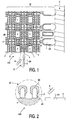
- Fig. 1 is a schematic top view of a packaged semiconductor device in a relevant stage in the manufacture of the device by means of a method in accordance with the invention.
- the stage shown in Fig. 1 corresponds with the singulation step of the method.
- a carrier 100 in this case of copper, comprises a number of die pads 1 on which a semiconductor crystal - not shown in the drawing - is present.
- the die pads 1 are surrounded by leads 2 which are separated from the die pad by a gap 3 in the carrier 100 and connected to parts of the carrier 100 which function as the sawing lanes 4 for a dicing blade 5 rotating around an axis 5A.
- the dicing blade 5 comprises a sintered metal with sharp cleaving diamond grains as described above.
- the semiconductor crystals are connected to the leads 2 to by means of wire-bonds that are also not shown in the drawing.
- a nozzle 6 close to the dicing blade 5 is a nozzle 6 through which a mixture of synthetic oil with water is directed to the dicing blade 5 during the dicing process.
- a mixture of 5 vol. % of Sintilo 82 of Castrol with (tap) water is used.
- a this stage the semiconductor crystals are covered by a mold material - not shown in the drawing - which is present in the area M of the carrier 100.
- the carrier 100 has been clamped during the molding process at the area C of the carrier 100 which is thus free of mold.
- the mold comprises here an epoxy material that is filled with glass up to 80 percent.
- the carrier 100 is provided with a number of features, which contributes to an optimal dicing in the method according to the invention. Firstly, the design of the carrier 100 is symmetrically along the sawing lanes 4. Secondly the copper of the carrier 100 is half-etched from the bottom side in a number of areas of the carrier 100 which are provided with a fine hatching in the Figs. In the sawing lanes 4 this half-etching reduces the amount of copper which is to be sawn. Thirdly the carrier 100 is provided with side-rail slots 7 where no copper is present. These are mainly positioned in the molding area M in front of the sawing lanes 4 were the dicing blade 5 will enter the carrier 100. These slots 7 are only shown in the Fig.
- the carrier 100 at one side of the carrier 100 but will be preferably present at all four sides of the carrier 100.
- the area 8 of the carrier 100 which connects a slot 7 with a sawing lane 4 is preferably half-etched. Further half-etched areas 9A,9B of the carrier 100 are present along side faces of the slots 7 and the leads 2 respectively.
- additional slots 17 which are positioned between slots 7 and which are also provided with an half-etched area 9C along there sides in order to anchor the mold to the carrier 100.
- Fig. 2 is a schematic top view of a detail of the device of Fig. 1 that is indicated therein with II: It shows a part of the sawing-lane 4 part of the carrier 100 together with two leads 2.
- the leads 2 are provided with half-etched areas 9B for anchoring and preventing unwanted vibrations of the carrier 100 during the dicing. Best results with respect to damage and wear of the dicing blade 5 and damage to the singulated semiconductor device are obtained if such half-etched areas are absent where the dicing blade 5 enters the leads 2.
- Such a side face 2A is preferably straight and plane and runs perpendicular to the face of the dicing blade 5 which enters the leads 2 during dicing. For this reason also a suitable radius of curvature is chosen where the side face 2A of the lead 2 changes to a sideface of the sawing lane (area) 4.
Landscapes
- Engineering & Computer Science (AREA)
- Mechanical Engineering (AREA)
- Dicing (AREA)
- Processing Of Stones Or Stones Resemblance Materials (AREA)
- Physical Vapour Deposition (AREA)
- Encapsulation Of And Coatings For Semiconductor Or Solid State Devices (AREA)
Claims (12)
- Ein Verfahren zur Herstellung eines verpackten Halbleiterbauelements, umfassend: einen Schritt des Vereinzelns eines Metallträgers (100), der mit mindestens einem Halbleiterkristall versehen ist, wobei der mindestens eine Halbleiterkristall mit einer Einkapselung versehen ist, in einer Zerteilungsvorrichtung, die mit einer Zerteilungsklinge (5) versehen ist, die Diamantkörner umfasst, wobei bei dem Vereinzelungsschritt die Zerteilungsklinge (5), während sie mit einem Kühlfluid gekühlt wird, die Einkapselung und den Metallträger (100) durchschneidet, um das mindestens eine Halbleiterbauelement zu vereinzeln, dadurch gekennzeichnet, dass eine die Reibungskraft vermindernde Kühlemulsion aus synthetischem Öl in Wasser während des Vereinzelungsschritts mittels der Zerteilungsklinge und unter Verwendung einer Düse (6) so aufgebracht wird, dass die Emulsion durch die Düse (6) auf die Zerteilungsklinge (5) gerichtet wird.
- Ein Verfahren nach Anspruch 1, gekennzeichnet durch die Verwendung von synthetischem Öl als einem Zusatz zu Kühlwasser als das die Reibungskraft vermindernde Kühlfluid in der Form einer Emulsion des Öls in Wasser.
- Ein Verfahren nach Anspruch 2, gekennzeichnet durch das Aufbringen des synthetischen Öls in einem Volumenprozentsatz im Bereich von 1 bis 10.
- Ein Verfahren nach Anspruch 1, 2 oder 3, gekennzeichnet durch die Verwendung einer Zerteilungsklinge (5) aus gesintertem Metall mit scharfen spaltenden Diamantkömem, wobei die scharfen spaltenden Diamantkörner in der Zerteilungsklinge in einer Konzentration aufgebracht sind, die kleiner oder gleich einer Maximalkonzentration ist, wobei die Maximalkonzentration durch die Konzentration definiert ist, bei welcher der gegenseitige Abstand zwischen den Diamantkörnern, die zum Schneiden beitragen, gerade groß genug ist, um die Entfernung von im Wesentlichen allem Sägemehl zu ermöglichen.
- Ein Verfahren nach Anspruch 4, gekennzeichnet durch das Aufbringen der scharfen spaltenden Diamantkörner in der Zerteilungsklinge (5) in einer Konzentration, die größer oder gleich einer Minimalkonzentration ist, wobei die Minimalkonzentration durch die Konzentration definiert ist, bei welcher die Zerteilungskraft pro Diamantkorn, das zum Schneiden beiträgt, gerade gering genug ist, um zu verhindern, dass das Diamantkorn aus der Zerteilungsklinge ausbricht.
- Ein Verfahren nach Anspruch 4 oder 5, gekennzeichnet durch das Aufbringen der scharfen spaltenden Diamantkörner mit einer Größe im Bereich von 20 bis 60 Mikrometern.
- Ein Verfahren nach einem der vorangehenden Ansprüche, gekennzeichnet durch das Aufbringen des Metallträgers (100) mit einer Gestaltung, die entlang von Sägespuren (4), entlang der die Zerteilungsklinge (5) den Träger (100) zerschneidet, symmetrisch ist.
- Ein Verfahren nach Anspruch 7, gekennzeichnet durch das Versehen von Seitenteilen (C) des Trägers (100) mit Schlitzen (7), die vor den Sägespuren (4) angeordnet sind.
- Ein Verfahren nach Anspruch 1, wobei der Metallträger eine Mehrzahl von Leitungen (2) umfasst, die sich in Sägespuren, entlang der die Zerteilungsklinge (5) den Träger (100) zerschneidet, hinein erstrecken.
- Ein Verfahren nach Anspruch 9, wobei die Leitungen (2) mit halbgeätzten Bereichen (9B) entlang ihren Seitenflächen zum Verankern des Trägers (100) an der Einkapselung und zum Verhindern unerwünschter Schwingungen des Trägers (100) während des Zerteilens versehen sind.
- Ein Verfahren nach Anspruch 10, wobei die halbgeätzten Bereiche (9B) an einer Stelle, wo die Zerteilungsklinge (5) in die Leitungen (2) eintritt, fehlen, so dass die Leitungen (2) an der Stelle mit einer Seitenfläche (2A) versehen sind, die beim Eintreten in die Leitungen (2) während des Zerteilens senkrecht zur Vorderseite der Zerteilungsklinge (5) verläuft.
- Ein Verfahren nach Anspruch 1 oder 7, wobei der Metallträger (100) in Sägespuren (4), entlang der die Zerteilungsklinge (5) den Träger (100) zerschneidet, mit einem halbgeätzten Bereich versehen ist, wobei die halbe Ätzung so erfolgt, dass die Einkapselung in den Sägespuren (4) auf beiden Seiten des Trägers (100) vorhanden ist.
Priority Applications (1)
| Application Number | Priority Date | Filing Date | Title |
|---|---|---|---|
| EP03784423A EP1549472B1 (de) | 2002-08-05 | 2003-07-31 | Verfahren zur herstellung einer verpackten halbleitervorrichtung, mit solch einem verfahren erhaltene verpackte halbleitervorrichtung und zur verwendung in solch einem verfahren geeigneter metallträger |
Applications Claiming Priority (4)
| Application Number | Priority Date | Filing Date | Title |
|---|---|---|---|
| EP02078269 | 2002-08-05 | ||
| EP02078269 | 2002-08-05 | ||
| EP03784423A EP1549472B1 (de) | 2002-08-05 | 2003-07-31 | Verfahren zur herstellung einer verpackten halbleitervorrichtung, mit solch einem verfahren erhaltene verpackte halbleitervorrichtung und zur verwendung in solch einem verfahren geeigneter metallträger |
| PCT/IB2003/003712 WO2004014626A1 (en) | 2002-08-05 | 2003-07-31 | Method and apparatus for manufacturing a packaged semiconductor device, packaged semiconductor device obtained with such a method and metal carrier suitable for use in such a method |
Publications (2)
| Publication Number | Publication Date |
|---|---|
| EP1549472A1 EP1549472A1 (de) | 2005-07-06 |
| EP1549472B1 true EP1549472B1 (de) | 2008-09-24 |
Family
ID=31502788
Family Applications (1)
| Application Number | Title | Priority Date | Filing Date |
|---|---|---|---|
| EP03784423A Expired - Lifetime EP1549472B1 (de) | 2002-08-05 | 2003-07-31 | Verfahren zur herstellung einer verpackten halbleitervorrichtung, mit solch einem verfahren erhaltene verpackte halbleitervorrichtung und zur verwendung in solch einem verfahren geeigneter metallträger |
Country Status (10)
| Country | Link |
|---|---|
| US (1) | US7115443B2 (de) |
| EP (1) | EP1549472B1 (de) |
| JP (1) | JP2005535140A (de) |
| KR (1) | KR20050042144A (de) |
| CN (1) | CN100557781C (de) |
| AT (1) | ATE409107T1 (de) |
| AU (1) | AU2003255956A1 (de) |
| DE (1) | DE60323758D1 (de) |
| TW (1) | TWI310960B (de) |
| WO (1) | WO2004014626A1 (de) |
Families Citing this family (3)
| Publication number | Priority date | Publication date | Assignee | Title |
|---|---|---|---|---|
| US7972940B2 (en) * | 2007-12-28 | 2011-07-05 | Micron Technology, Inc. | Wafer processing |
| CN102009433B (zh) * | 2010-11-03 | 2012-11-21 | 江苏省宜兴电子器件总厂 | 陶瓷外壳刻槽模具及用该模具加工无引线陶瓷外壳的方法 |
| CN105471405B (zh) * | 2014-09-30 | 2018-08-28 | 日本特殊陶业株式会社 | 布线基板及多连片式布线基板 |
Citations (1)
| Publication number | Priority date | Publication date | Assignee | Title |
|---|---|---|---|---|
| CN1296871A (zh) * | 1999-11-22 | 2001-05-30 | 住友特殊金属株式会社 | 工件切削装置和切削方法 |
Family Cites Families (20)
| Publication number | Priority date | Publication date | Assignee | Title |
|---|---|---|---|---|
| JPS62114254A (ja) * | 1985-11-13 | 1987-05-26 | Mitsui Haitetsuku:Kk | リ−ドフレ−ムの製造方法 |
| DE4309134C2 (de) | 1993-03-22 | 1999-03-04 | Wilfried Wahl | Verfahren zur Schmierung und Kühlung von Schneiden und/oder Werkstücken bei zerspanenden Arbeitsprozessen |
| US5682062A (en) * | 1995-06-05 | 1997-10-28 | Harris Corporation | System for interconnecting stacked integrated circuits |
| US5646315A (en) * | 1995-06-07 | 1997-07-08 | National Starch And Chemical Investment Holding Corporation | Polyglydicylphenyl ethers of alkyloxy chains for use in microelectronics adhesives |
| US6284566B1 (en) * | 1996-05-17 | 2001-09-04 | National Semiconductor Corporation | Chip scale package and method for manufacture thereof |
| US5832585A (en) * | 1996-08-13 | 1998-11-10 | National Semiconductor Corporation | Method of separating micro-devices formed on a substrate |
| KR100222299B1 (ko) * | 1996-12-16 | 1999-10-01 | 윤종용 | 웨이퍼 레벨 칩 스케일 패키지 및 그의 제조 방법 |
| KR100225909B1 (ko) * | 1997-05-29 | 1999-10-15 | 윤종용 | 웨이퍼 소잉 장치 |
| EP0886144B1 (de) * | 1997-06-19 | 2006-09-06 | STMicroelectronics S.r.l. | Hermetisch abgeschlossener Sensor mit beweglicher Mikrostruktur |
| SG70097A1 (en) * | 1997-08-15 | 2000-01-25 | Disio Corp | Apparatus and method for machining workpieces by flushing working liquid to the tool-and-workpiece interface |
| JP4396953B2 (ja) * | 1998-08-26 | 2010-01-13 | 三星電子株式会社 | レーザ切断装置および切断方法 |
| ES2288023T3 (es) * | 1998-11-20 | 2007-12-16 | Sankyo Diamond Industrial Co., Ltd. | Disco adiamantado y procedimiento para fabricar el mismo. |
| JP3398721B2 (ja) * | 1999-05-20 | 2003-04-21 | アムコー テクノロジー コリア インコーポレーティド | 半導体パッケージ及びその製造方法 |
| US6413150B1 (en) * | 1999-05-27 | 2002-07-02 | Texas Instruments Incorporated | Dual dicing saw blade assembly and process for separating devices arrayed a substrate |
| US6400004B1 (en) * | 2000-08-17 | 2002-06-04 | Advanced Semiconductor Engineering, Inc. | Leadless semiconductor package |
| US6467278B1 (en) * | 2000-11-15 | 2002-10-22 | National Semiconductor Corporation | Cooling for singulation of composite materials in molded semiconductor packages |
| JP3619773B2 (ja) * | 2000-12-20 | 2005-02-16 | 株式会社ルネサステクノロジ | 半導体装置の製造方法 |
| JP3628971B2 (ja) | 2001-02-15 | 2005-03-16 | 松下電器産業株式会社 | リードフレーム及びそれを用いた樹脂封止型半導体装置の製造方法 |
| EP1435112A2 (de) * | 2001-06-19 | 2004-07-07 | Koninklijke Philips Electronics N.V. | Herstellungsmethode eines halbleiterbauteils und halbleiterbauteil |
| US6849523B2 (en) * | 2003-03-12 | 2005-02-01 | Taiwan Semiconductor Manufacturing Co., Ltd | Process for separating dies on a wafer |
-
2003
- 2003-07-31 AT AT03784423T patent/ATE409107T1/de not_active IP Right Cessation
- 2003-07-31 JP JP2004527236A patent/JP2005535140A/ja active Pending
- 2003-07-31 WO PCT/IB2003/003712 patent/WO2004014626A1/en not_active Ceased
- 2003-07-31 EP EP03784423A patent/EP1549472B1/de not_active Expired - Lifetime
- 2003-07-31 KR KR1020057001990A patent/KR20050042144A/ko not_active Ceased
- 2003-07-31 DE DE60323758T patent/DE60323758D1/de not_active Expired - Lifetime
- 2003-07-31 US US10/523,534 patent/US7115443B2/en not_active Expired - Lifetime
- 2003-07-31 AU AU2003255956A patent/AU2003255956A1/en not_active Abandoned
- 2003-07-31 CN CNB03818754XA patent/CN100557781C/zh not_active Expired - Fee Related
- 2003-08-01 TW TW092121150A patent/TWI310960B/zh active
Patent Citations (2)
| Publication number | Priority date | Publication date | Assignee | Title |
|---|---|---|---|---|
| CN1296871A (zh) * | 1999-11-22 | 2001-05-30 | 住友特殊金属株式会社 | 工件切削装置和切削方法 |
| US6463920B1 (en) * | 1999-11-22 | 2002-10-15 | Sumitomo Special Metals Co., Ltd. | Work cutting apparatus and work cutting method |
Also Published As
| Publication number | Publication date |
|---|---|
| AU2003255956A1 (en) | 2004-02-25 |
| US7115443B2 (en) | 2006-10-03 |
| EP1549472A1 (de) | 2005-07-06 |
| WO2004014626A1 (en) | 2004-02-19 |
| US20050255630A1 (en) | 2005-11-17 |
| DE60323758D1 (de) | 2008-11-06 |
| TWI310960B (en) | 2009-06-11 |
| JP2005535140A (ja) | 2005-11-17 |
| TW200416776A (en) | 2004-09-01 |
| KR20050042144A (ko) | 2005-05-04 |
| ATE409107T1 (de) | 2008-10-15 |
| CN1675041A (zh) | 2005-09-28 |
| CN100557781C (zh) | 2009-11-04 |
Similar Documents
| Publication | Publication Date | Title |
|---|---|---|
| US6294439B1 (en) | Method of dividing a wafer and method of manufacturing a semiconductor device | |
| CN1296988C (zh) | 用于保持晶片上的接合焊垫超洁净的方法 | |
| US6023094A (en) | Semiconductor wafer having a bottom surface protective coating | |
| US6609965B2 (en) | Cutting blade | |
| KR100452661B1 (ko) | 웨이퍼의 분할 방법 및 반도체 장치의 제조 방법 | |
| TW201440179A (zh) | 半導體裝置、半導體裝置之製造方法 | |
| US20140138805A1 (en) | System for No-Lead Integrated Circuit Packages Without Tape Frame | |
| US3078559A (en) | Method for preparing semiconductor elements | |
| US7115443B2 (en) | Method and apparatus for manufacturing a packaged semiconductor device, packaged semiconductor device obtained with such a method and metal carrier suitable for use in such a method | |
| US20060261445A1 (en) | Integrated circuit device with treated perimeter edge | |
| JP2003159642A (ja) | ワーク切断方法およびマルチワイヤソーシステム | |
| US7086394B2 (en) | Grindable self-cleaning singulation saw blade and method | |
| US20030047177A1 (en) | Method for cutting ingots for use with a wire cutting apparatus | |
| CN112338802B (zh) | 修锐板以及切削刀具的修锐方法 | |
| CN1163948C (zh) | 晶片切割研磨制作方法 | |
| JP2000277550A (ja) | 半導体装置およびその製造方法 | |
| US20240091968A1 (en) | Blade for sawing a panel level package and method of sawing a panel level package using the same | |
| JPH0831773A (ja) | 半導体装置とダイシングブレードおよびこれを用いたダイシング方法 | |
| RU2108225C1 (ru) | Способ резки полупроводниковых слитков на пластины | |
| KR940008558B1 (ko) | 반도체 칩 분리방법 및 그 장치 | |
| JPH02152765A (ja) | ワイヤソーによる切断加工方法 | |
| KR20190067449A (ko) | 지석을 이용한 와이어 절삭 장치 | |
| KR20030079293A (ko) | 웨이퍼의 가공방법 | |
| JPH06216241A (ja) | ウェーハ等の切削方法 | |
| JPH04361556A (ja) | ダイシング方法 |
Legal Events
| Date | Code | Title | Description |
|---|---|---|---|
| PUAI | Public reference made under article 153(3) epc to a published international application that has entered the european phase |
Free format text: ORIGINAL CODE: 0009012 |
|
| 17P | Request for examination filed |
Effective date: 20050307 |
|
| AK | Designated contracting states |
Kind code of ref document: A1 Designated state(s): AT BE BG CH CY CZ DE DK EE ES FI FR GB GR HU IE IT LI LU MC NL PT RO SE SI SK TR |
|
| AX | Request for extension of the european patent |
Extension state: AL LT LV MK |
|
| DAX | Request for extension of the european patent (deleted) | ||
| RAP1 | Party data changed (applicant data changed or rights of an application transferred) |
Owner name: NXP B.V. |
|
| GRAP | Despatch of communication of intention to grant a patent |
Free format text: ORIGINAL CODE: EPIDOSNIGR1 |
|
| RTI1 | Title (correction) |
Free format text: METHOD FOR MANUFACTURING A PACKAGED SEMICONDUCTOR DEVICE, PACKAGED SEMICONDUCTOR DEVICE OBTAINED WITH SUCH A METHOD AND METAL CARRIER SUITABLE FOR USE IN SUCH A METHOD |
|
| GRAS | Grant fee paid |
Free format text: ORIGINAL CODE: EPIDOSNIGR3 |
|
| GRAA | (expected) grant |
Free format text: ORIGINAL CODE: 0009210 |
|
| AK | Designated contracting states |
Kind code of ref document: B1 Designated state(s): AT BE BG CH CY CZ DE DK EE ES FI FR GB GR HU IE IT LI LU MC NL PT RO SE SI SK TR |
|
| REG | Reference to a national code |
Ref country code: GB Ref legal event code: FG4D |
|
| REG | Reference to a national code |
Ref country code: CH Ref legal event code: EP |
|
| REG | Reference to a national code |
Ref country code: IE Ref legal event code: FG4D |
|
| REF | Corresponds to: |
Ref document number: 60323758 Country of ref document: DE Date of ref document: 20081106 Kind code of ref document: P |
|
| PG25 | Lapsed in a contracting state [announced via postgrant information from national office to epo] |
Ref country code: FI Free format text: LAPSE BECAUSE OF FAILURE TO SUBMIT A TRANSLATION OF THE DESCRIPTION OR TO PAY THE FEE WITHIN THE PRESCRIBED TIME-LIMIT Effective date: 20080924 Ref country code: SI Free format text: LAPSE BECAUSE OF FAILURE TO SUBMIT A TRANSLATION OF THE DESCRIPTION OR TO PAY THE FEE WITHIN THE PRESCRIBED TIME-LIMIT Effective date: 20080924 Ref country code: AT Free format text: LAPSE BECAUSE OF FAILURE TO SUBMIT A TRANSLATION OF THE DESCRIPTION OR TO PAY THE FEE WITHIN THE PRESCRIBED TIME-LIMIT Effective date: 20080924 |
|
| PG25 | Lapsed in a contracting state [announced via postgrant information from national office to epo] |
Ref country code: BE Free format text: LAPSE BECAUSE OF FAILURE TO SUBMIT A TRANSLATION OF THE DESCRIPTION OR TO PAY THE FEE WITHIN THE PRESCRIBED TIME-LIMIT Effective date: 20080924 |
|
| PG25 | Lapsed in a contracting state [announced via postgrant information from national office to epo] |
Ref country code: ES Free format text: LAPSE BECAUSE OF FAILURE TO SUBMIT A TRANSLATION OF THE DESCRIPTION OR TO PAY THE FEE WITHIN THE PRESCRIBED TIME-LIMIT Effective date: 20090104 Ref country code: BG Free format text: LAPSE BECAUSE OF FAILURE TO SUBMIT A TRANSLATION OF THE DESCRIPTION OR TO PAY THE FEE WITHIN THE PRESCRIBED TIME-LIMIT Effective date: 20081224 |
|
| PG25 | Lapsed in a contracting state [announced via postgrant information from national office to epo] |
Ref country code: SK Free format text: LAPSE BECAUSE OF FAILURE TO SUBMIT A TRANSLATION OF THE DESCRIPTION OR TO PAY THE FEE WITHIN THE PRESCRIBED TIME-LIMIT Effective date: 20080924 Ref country code: PT Free format text: LAPSE BECAUSE OF FAILURE TO SUBMIT A TRANSLATION OF THE DESCRIPTION OR TO PAY THE FEE WITHIN THE PRESCRIBED TIME-LIMIT Effective date: 20090224 Ref country code: RO Free format text: LAPSE BECAUSE OF FAILURE TO SUBMIT A TRANSLATION OF THE DESCRIPTION OR TO PAY THE FEE WITHIN THE PRESCRIBED TIME-LIMIT Effective date: 20080924 Ref country code: CZ Free format text: LAPSE BECAUSE OF FAILURE TO SUBMIT A TRANSLATION OF THE DESCRIPTION OR TO PAY THE FEE WITHIN THE PRESCRIBED TIME-LIMIT Effective date: 20080924 |
|
| PG25 | Lapsed in a contracting state [announced via postgrant information from national office to epo] |
Ref country code: DK Free format text: LAPSE BECAUSE OF FAILURE TO SUBMIT A TRANSLATION OF THE DESCRIPTION OR TO PAY THE FEE WITHIN THE PRESCRIBED TIME-LIMIT Effective date: 20080924 Ref country code: EE Free format text: LAPSE BECAUSE OF FAILURE TO SUBMIT A TRANSLATION OF THE DESCRIPTION OR TO PAY THE FEE WITHIN THE PRESCRIBED TIME-LIMIT Effective date: 20080924 |
|
| PLBE | No opposition filed within time limit |
Free format text: ORIGINAL CODE: 0009261 |
|
| STAA | Information on the status of an ep patent application or granted ep patent |
Free format text: STATUS: NO OPPOSITION FILED WITHIN TIME LIMIT |
|
| PG25 | Lapsed in a contracting state [announced via postgrant information from national office to epo] |
Ref country code: IT Free format text: LAPSE BECAUSE OF FAILURE TO SUBMIT A TRANSLATION OF THE DESCRIPTION OR TO PAY THE FEE WITHIN THE PRESCRIBED TIME-LIMIT Effective date: 20080924 |
|
| 26N | No opposition filed |
Effective date: 20090625 |
|
| PG25 | Lapsed in a contracting state [announced via postgrant information from national office to epo] |
Ref country code: SE Free format text: LAPSE BECAUSE OF FAILURE TO SUBMIT A TRANSLATION OF THE DESCRIPTION OR TO PAY THE FEE WITHIN THE PRESCRIBED TIME-LIMIT Effective date: 20081224 |
|
| PG25 | Lapsed in a contracting state [announced via postgrant information from national office to epo] |
Ref country code: MC Free format text: LAPSE BECAUSE OF NON-PAYMENT OF DUE FEES Effective date: 20090731 |
|
| REG | Reference to a national code |
Ref country code: CH Ref legal event code: PL |
|
| REG | Reference to a national code |
Ref country code: IE Ref legal event code: MM4A |
|
| PG25 | Lapsed in a contracting state [announced via postgrant information from national office to epo] |
Ref country code: LI Free format text: LAPSE BECAUSE OF NON-PAYMENT OF DUE FEES Effective date: 20090731 Ref country code: CH Free format text: LAPSE BECAUSE OF NON-PAYMENT OF DUE FEES Effective date: 20090731 |
|
| PG25 | Lapsed in a contracting state [announced via postgrant information from national office to epo] |
Ref country code: IE Free format text: LAPSE BECAUSE OF NON-PAYMENT OF DUE FEES Effective date: 20090731 |
|
| PG25 | Lapsed in a contracting state [announced via postgrant information from national office to epo] |
Ref country code: GR Free format text: LAPSE BECAUSE OF FAILURE TO SUBMIT A TRANSLATION OF THE DESCRIPTION OR TO PAY THE FEE WITHIN THE PRESCRIBED TIME-LIMIT Effective date: 20081225 |
|
| PGFP | Annual fee paid to national office [announced via postgrant information from national office to epo] |
Ref country code: NL Payment date: 20100707 Year of fee payment: 8 |
|
| PG25 | Lapsed in a contracting state [announced via postgrant information from national office to epo] |
Ref country code: LU Free format text: LAPSE BECAUSE OF NON-PAYMENT OF DUE FEES Effective date: 20090731 |
|
| PG25 | Lapsed in a contracting state [announced via postgrant information from national office to epo] |
Ref country code: HU Free format text: LAPSE BECAUSE OF FAILURE TO SUBMIT A TRANSLATION OF THE DESCRIPTION OR TO PAY THE FEE WITHIN THE PRESCRIBED TIME-LIMIT Effective date: 20090325 |
|
| PG25 | Lapsed in a contracting state [announced via postgrant information from national office to epo] |
Ref country code: TR Free format text: LAPSE BECAUSE OF FAILURE TO SUBMIT A TRANSLATION OF THE DESCRIPTION OR TO PAY THE FEE WITHIN THE PRESCRIBED TIME-LIMIT Effective date: 20080924 |
|
| PG25 | Lapsed in a contracting state [announced via postgrant information from national office to epo] |
Ref country code: CY Free format text: LAPSE BECAUSE OF FAILURE TO SUBMIT A TRANSLATION OF THE DESCRIPTION OR TO PAY THE FEE WITHIN THE PRESCRIBED TIME-LIMIT Effective date: 20080924 |
|
| REG | Reference to a national code |
Ref country code: NL Ref legal event code: V1 Effective date: 20120201 |
|
| PG25 | Lapsed in a contracting state [announced via postgrant information from national office to epo] |
Ref country code: NL Free format text: LAPSE BECAUSE OF NON-PAYMENT OF DUE FEES Effective date: 20120201 |
|
| PGFP | Annual fee paid to national office [announced via postgrant information from national office to epo] |
Ref country code: GB Payment date: 20120629 Year of fee payment: 10 |
|
| GBPC | Gb: european patent ceased through non-payment of renewal fee |
Effective date: 20130731 |
|
| PG25 | Lapsed in a contracting state [announced via postgrant information from national office to epo] |
Ref country code: GB Free format text: LAPSE BECAUSE OF NON-PAYMENT OF DUE FEES Effective date: 20130731 |
|
| REG | Reference to a national code |
Ref country code: FR Ref legal event code: PLFP Year of fee payment: 13 |
|
| REG | Reference to a national code |
Ref country code: FR Ref legal event code: PLFP Year of fee payment: 14 |
|
| REG | Reference to a national code |
Ref country code: FR Ref legal event code: PLFP Year of fee payment: 15 |
|
| REG | Reference to a national code |
Ref country code: FR Ref legal event code: PLFP Year of fee payment: 16 |
|
| PGFP | Annual fee paid to national office [announced via postgrant information from national office to epo] |
Ref country code: FR Payment date: 20200623 Year of fee payment: 18 |
|
| PGFP | Annual fee paid to national office [announced via postgrant information from national office to epo] |
Ref country code: DE Payment date: 20200622 Year of fee payment: 18 |
|
| REG | Reference to a national code |
Ref country code: DE Ref legal event code: R119 Ref document number: 60323758 Country of ref document: DE |
|
| PG25 | Lapsed in a contracting state [announced via postgrant information from national office to epo] |
Ref country code: DE Free format text: LAPSE BECAUSE OF NON-PAYMENT OF DUE FEES Effective date: 20220201 |
|
| PG25 | Lapsed in a contracting state [announced via postgrant information from national office to epo] |
Ref country code: FR Free format text: LAPSE BECAUSE OF NON-PAYMENT OF DUE FEES Effective date: 20210731 |