EP1548826A1 - Chipkontaktlayout - Google Patents
Chipkontaktlayout Download PDFInfo
- Publication number
- EP1548826A1 EP1548826A1 EP04257964A EP04257964A EP1548826A1 EP 1548826 A1 EP1548826 A1 EP 1548826A1 EP 04257964 A EP04257964 A EP 04257964A EP 04257964 A EP04257964 A EP 04257964A EP 1548826 A1 EP1548826 A1 EP 1548826A1
- Authority
- EP
- European Patent Office
- Prior art keywords
- lands
- integrated circuit
- circuit device
- bumps
- circuit board
- Prior art date
- Legal status (The legal status is an assumption and is not a legal conclusion. Google has not performed a legal analysis and makes no representation as to the accuracy of the status listed.)
- Granted
Links
Images






Classifications
-
- H—ELECTRICITY
- H10—SEMICONDUCTOR DEVICES; ELECTRIC SOLID-STATE DEVICES NOT OTHERWISE PROVIDED FOR
- H10W—GENERIC PACKAGES, INTERCONNECTIONS, CONNECTORS OR OTHER CONSTRUCTIONAL DETAILS OF DEVICES COVERED BY CLASS H10
- H10W70/00—Package substrates; Interposers; Redistribution layers [RDL]
- H10W70/60—Insulating or insulated package substrates; Interposers; Redistribution layers
- H10W70/67—Insulating or insulated package substrates; Interposers; Redistribution layers characterised by their insulating layers or insulating parts
- H10W70/688—Flexible insulating substrates
-
- B—PERFORMING OPERATIONS; TRANSPORTING
- B41—PRINTING; LINING MACHINES; TYPEWRITERS; STAMPS
- B41J—TYPEWRITERS; SELECTIVE PRINTING MECHANISMS, i.e. MECHANISMS PRINTING OTHERWISE THAN FROM A FORME; CORRECTION OF TYPOGRAPHICAL ERRORS
- B41J2/00—Typewriters or selective printing mechanisms characterised by the printing or marking process for which they are designed
- B41J2/005—Typewriters or selective printing mechanisms characterised by the printing or marking process for which they are designed characterised by bringing liquid or particles selectively into contact with a printing material
- B41J2/01—Ink jet
- B41J2/135—Nozzles
- B41J2/14—Structure thereof only for on-demand ink jet heads
- B41J2/14201—Structure of print heads with piezoelectric elements
- B41J2/14209—Structure of print heads with piezoelectric elements of finger type, chamber walls consisting integrally of piezoelectric material
-
- H—ELECTRICITY
- H10—SEMICONDUCTOR DEVICES; ELECTRIC SOLID-STATE DEVICES NOT OTHERWISE PROVIDED FOR
- H10W—GENERIC PACKAGES, INTERCONNECTIONS, CONNECTORS OR OTHER CONSTRUCTIONAL DETAILS OF DEVICES COVERED BY CLASS H10
- H10W70/00—Package substrates; Interposers; Redistribution layers [RDL]
- H10W70/60—Insulating or insulated package substrates; Interposers; Redistribution layers
- H10W70/62—Insulating or insulated package substrates; Interposers; Redistribution layers characterised by their interconnections
- H10W70/65—Shapes or dispositions of interconnections
-
- B—PERFORMING OPERATIONS; TRANSPORTING
- B41—PRINTING; LINING MACHINES; TYPEWRITERS; STAMPS
- B41J—TYPEWRITERS; SELECTIVE PRINTING MECHANISMS, i.e. MECHANISMS PRINTING OTHERWISE THAN FROM A FORME; CORRECTION OF TYPOGRAPHICAL ERRORS
- B41J2/00—Typewriters or selective printing mechanisms characterised by the printing or marking process for which they are designed
- B41J2/005—Typewriters or selective printing mechanisms characterised by the printing or marking process for which they are designed characterised by bringing liquid or particles selectively into contact with a printing material
- B41J2/01—Ink jet
- B41J2/135—Nozzles
- B41J2/14—Structure thereof only for on-demand ink jet heads
- B41J2002/14491—Electrical connection
-
- H—ELECTRICITY
- H10—SEMICONDUCTOR DEVICES; ELECTRIC SOLID-STATE DEVICES NOT OTHERWISE PROVIDED FOR
- H10P—GENERIC PROCESSES OR APPARATUS FOR THE MANUFACTURE OR TREATMENT OF DEVICES COVERED BY CLASS H10
- H10P74/00—Testing or measuring during manufacture or treatment of wafers, substrates or devices
- H10P74/27—Structural arrangements therefor
- H10P74/273—Interconnections for measuring or testing, e.g. probe pads
-
- H—ELECTRICITY
- H10—SEMICONDUCTOR DEVICES; ELECTRIC SOLID-STATE DEVICES NOT OTHERWISE PROVIDED FOR
- H10W—GENERIC PACKAGES, INTERCONNECTIONS, CONNECTORS OR OTHER CONSTRUCTIONAL DETAILS OF DEVICES COVERED BY CLASS H10
- H10W72/00—Interconnections or connectors in packages
Definitions
- the invention relates to a printed circuit board on which devices of integrated circuits are mounted and an inkjet head employing such a printed circuit board.
- bare chip mounting is a technology that bumps, which are protruding electrodes disposed on lower surfaces of the bare chips and formed by, for example, gold, are bonded to lands, which are flat-surface electrodes formed on the printed circuit boards, by high temperature and high pressure, so that the bare chips are mounted on the printed circuit boards. Bumps of bare chips and corresponding lands are minute having a width of about 30 ⁇ m. In bare chip mounting, precise positioning and precise measurement of pressure to be applied are required.
- Some bare chips are structured such that bumps are arranged near each side of the bare chips and the number of bumps arranged near one side is greatly different compared with the number of bumps arranged near the one opposite to it.
- the number of bumps on the input portion side is less than the number of bumps on the output portion side.
- the bare chip described above has a reliability problem when mounted to the printed circuit board.
- the invention provides a printed circuit board capable of increasing reliability to mount a bare chip thereon even if the number of bumps is different on sides opposite to each other, and an inkjet head for use with such a printed circuit board.
- a printed circuit board includes a plurality of first lands, a first wiring pattern, a plurality of second lands, a second wiring pattern, and an at least one third land.
- the plurality of first lands are arranged to correspond to a plurality of first bumps on an integrated circuit device having a first side and a second side facing each other when the integrated circuit device is mounted on the printed circuit board.
- the plurality of first bumps are arranged along the first side of the integrated circuit device.
- the plurality of first lands is used for individually inputting or outputting an electrical signal with respect to the integrated circuit device via the plurality of first bumps when the integrated circuit device is mounted on the printed circuit board.
- the first wiring pattern is connected to the plurality of first lands.
- the plurality of second lands are arranged to correspond to a plurality of second bumps arranged along the second side of the integrated circuit device when the integrated circuit device is mounted on the printed circuit board.
- the plurality of second lands is less than the plurality of first lands in number.
- the plurality of second lands is used for individually inputting or outputting the electrical signal with respect to the integrated circuit device via the plurality of second bumps when the integrated circuit device is mounted on the printed circuit board.
- the second wiring pattern is connected to the plurality of second lands.
- the at least one third land is disposed to correspond to an at least one third bump disposed at least closer to and, hence, optionally in, a row formed by the plurality of second bumps than a row formed by the plurality of first bumps on the integrated circuit device when the integrated circuit device is mounted on the printed circuit board.
- the at least one third land has an area larger than each one of the plurality of first lands.
- the at least one third land is not used for inputting and outputting the electrical signal with respect to the integrated circuit device via the at least one third bump when the integrated circuit device is mounted on the printed circuit board.
- the integrated circuit device is a rectangle.
- the plurality of first lands may be arranged substantially linearly so as to correspond to the plurality of first bumps arranged substantially linearly along the first side of the integrated circuit device when the integrated circuit device is mounted on the printed circuit board.
- the plurality of second lands may be arranged substantially linearly so as to correspond to the plurality of second bumps arranged substantially linearly along the second side of the integrated circuit device when the integrated circuit device is mounted on the printed circuit board.
- the at least one third land having an area larger than each one of the plurality of first lands is connected to the at least one third bump closer to the row of the plurality of second lands than the row of the plurality of first lands.
- an entire area where bumps and the corresponding lands are bonded becomes widened, so that the bonding strength can be entirely increased.
- the at least one third land may be disposed in the row formed by the plurality of second lands so as to correspond to the at least one third bump arranged in the row formed by the plurality of second bumps of the integrated circuit device when the integrated circuit device is mounted on the printed circuit board.
- a plurality of third lands may be arranged in the row formed by the plurality of second lands so as to correspond to a plurality of third bumps arranged in the row formed by the plurality of second bumps of the integrated circuit device when the integrated circuit device is mounted on the printed circuit board, and a sum of areas of the plurality of first lands is substantially the same as a sum of areas of the plurality of second lands and the plurality of third lands.
- connection strength can be entirely increased on the side of the plurality of second lands.
- the at least one third bump may be a test bump used for a functional test of the integrated circuit device.
- test bump which is previously included in the device is bonded to the third land as the third bump, only providing the test bump can increase the reliability to mount the integrated circuit device on the printed circuit board only.
- the printed circuit board may further include an at least one fourth land disposed between a row formed by the plurality of first lands and the row formed by the plurality of second lands so as to correspond to an at least one fourth bump disposed between the row formed by the plurality of first bumps and the row formed by the plurality of second bumps.
- the at least one fourth land may be used for inputting or outputting the electrical signal with respect to the integrated circuit device via the at least one fourth bump when the integrated circuit device is mounted on the printed circuit board.
- a plurality of fourth lands may be arranged between the row formed by the plurality of first lands and the row formed by the plurality of second lands so as to correspond to a plurality of fourth bumps arranged between the row formed by the plurality of first bumps and the row formed by the plurality of second bumps of the integrated circuit device when the integrated circuit device is mounted on the printed circuit board.
- the at least one fourth bump arranged between the row formed by the plurality of first lands and the row formed by the plurality of second lands is connected to the at least one fourth land, the sum of areas where the bumps and lands are connected becomes great, thereby helping to increase the connection strength entirely.
- the printed circuit board may further include a third wiring pattern that extends to connect the plurality of fourth lands to each other within an area covered by the integrated circuit device when the integrated circuit device is mounted on the printed circuit board.
- the third wiring pattern may extend so as to pass at least one of a position corresponding to a third side of the integrated circuit device and a position corresponding to a fourth side of the integrated circuit device beyond the area covered by the integrated circuit device.
- the third wiring pattern may extend parallel to the row formed by the plurality of first lands and the row formed by the plurality of second lands in the area covered by the integrated circuit device.
- the third wiring pattern may supply a ground potential to the integrated circuit device via the plurality of fourth bumps when the integrated circuit device is mounted on the printed circuit board.
- the printed circuit board may further include a fifth land and a fourth wiring pattern.
- the fifth land may be disposed between the row formed by the plurality of first lands and the row formed by the plurality of second lands to correspond to a fifth bump disposed between the row formed by the plurality of first bumps and the row formed by the plurality of second bumps in the integrated circuit device when the integrated circuit device is mounted on the printed circuit board.
- the fourth wiring pattern may extend to be connected to the fifth land in the area covered by the integrated circuit device when the integrated circuit device is mounted on the printed circuit board.
- the fourth wiring pattern may supply power to the integrated circuit device via the fifth bump when the integrated circuit device is mounted on the printed circuit board, and the third wiring pattern and the fourth wiring pattern may be disposed adjacently to and parallel to each other in the area covered by the integrated circuit device.
- the third wiring pattern serves as a shield of the forth wiring pattern, thereby reducing the power noise.
- the plurality of first lands are connected to the plurality of first bumps of the integrated circuit device
- the plurality of second lands are connected to the plurality of second bumps of the integrated circuit device
- the at least one third land is connected to the at least one third bump of the integrated circuit device.
- a printed circuit board may be used in an inkjet head.
- the inkjet head may further include a passage unit having a plurality of passages each passing a pressure chamber and extending to a nozzle; and an actuator unit fixed to the passage unit, the actuator unit changing a volume of the pressure chamber.
- the printed circuit board is capable of applying an electrical signal to change the volume of the pressure chamber to the actuator unit via the integrated circuit device.
- the first wiring pattern is connected to the actuator unit.
- an inkjet head can be provided with high reliability even if the number of nozzles becomes great, and the number of second bumps is less than the number of first bumps.
- An inkjet printer 101 shown in FIG. 1 is a color inkjet printer including four inkjet heads 1.
- the inkjet printer 101 is provided with a sheet feed portion 102 on the left side of the drawing and a sheet ejection portion 103 on the right side.
- a sheet feed path where a sheet of paper is fed from the sheet feed portion 102 to the sheet ejection portion 103.
- a pair of sheet feed rollers 105a, 105b are disposed at a downstream side directly from the sheet feed portion 102.
- the sheet feed rollers 105a, 105b pick up a sheet of paper therebetween and feed it in from left to right in FIG 1.
- two belt rollers 106, 107, a conveyor belt 108 looped around the belt rollers 106, 107, and a motor (not shown) that drives the belt rollers 106, 107 are disposed.
- An outer surface of the conveyor belt 108, that is a carrying surface, is coated with silicone.
- a sheet conveyed by the sheet feed rollers 105a, 105b is held by the carrying surface of the conveyor belt 108 with its adhesion and conveyed toward the downstream side (rightward) by the belt roller 106 rotating in a clockwise direction (in a direction of an arrow 104).
- Each of the four inkjet heads 1 includes, at a lower end thereof, a head body 70 having a rectangular plane.
- the inkjet heads 1 are arranged adjacent to each other such that a longitudinal direction of the head body (a main scanning direction; a direction vertical to a sheet of FIG 1) is perpendicular to a sheet feed direction.
- the inkjet heads I are line heads.
- a bottom surface of each head body 70 faces to the sheet feed path, and is formed as an ejection surface with a plurality of nozzles having a minute diameter.
- the inkjet heads 1 eject cyan, magenta, yellow and black inks from the corresponding head bodies 70. Inks of each color are ejected from the nozzles onto an upper surface or a printed surface of the sheet being conveyed, and thus a desired color image is formed on the sheet.
- the inkjet heads 1 will be described with reference to FIGS. 2 and 3. As each inkjet head 1 is identical in shape, structure and operation except that it contains a different color of ink, the following description will be made with respect to one inkjet head 1.
- the inkjet head 1 includes the head body 70 having a rectangular plane, which extends in the main scanning direction to eject ink onto a sheet, and a base block 71, which is disposed over the head body 70 and formed with two ink reservoirs 3 providing ink passages through which ink is supplied to the head body 70.
- the head body 70 includes a passage unit 4 and actuator units 21.
- the passage unit 4 is provided with a plurality of ink passages, each communicated to a corresponding one of the nozzles.
- the actuator units 21 are bonded over the passage unit 4 in a face-to-face relation.
- the ink reservoirs 3 in the base block 71 are communicated to the passage unit 4 at an opening of a lower surface 73, such that ink is supplied from the ink reservoirs 3 to the ink passages formed in the passage unit 4.
- the ink passages individually include pressure chambers where pressure is generated to eject ink from the nozzles.
- the actuator unit 21 is used to generate pressure in each pressure chamber of the ink passages, and structured so as to hold a piezoelectric sheet with a common electrode that maintains ground potential and a plurality of individual electrodes, each disposed to be opposed to one of the pressure chambers.
- the piezoelectric sheet is made of a ceramic material of lead zirconate titanate (PZT) having ferroelectricity.
- PZT lead zirconate titanate
- the base block 71 is adhesively fixed in a hollow formed at a lower surface of a base portion 72a of the holder 72.
- the holder 72 is provided with the base portion 72a and a pair of projecting portions 72b, which extend from the base portion 72a in an orthogonal direction thereto at a predetermined distance away from each other.
- each of flexible printed circuits, FPCs, 50 is connected to the individual electrodes and extends to either one side of the inkjet head 1.
- the FPCs 50 are thin printed circuit boards functioning as a power feed member.
- the FPCs 50 bonded to the actuator units 21 are placed, via elastic members 83 such as sponge, over and along the projecting portions 72b of the holder 72.
- driver ICs 80 which drive the actuator units 21, are mounted.
- Heat sinks 82 are disposed on outer surfaces of the driver ICs 80.
- Boards 81 are disposed above the corresponding driver ICs 80 and heat sinks 82.
- the boards 81 are connected to the corresponding FPCs 50.
- the top surface of the heat sink 82 and the board 81, and the bottom surface of the heat sink 82 and the FPC 50 are bonded with sealing members 84 respectively.
- the boards 81 are control circuit boards that control the actuator units 21 according to directions from a controller (not shown) to form a desired image on a recording medium. Conductive patterns formed on the boards 81 are electrically connected to the driver ICs 80 via the FPCs 50. Control signals are outputted from the boards 81 to the driver ICs 80, thereby controlling the actuator units 21.
- the driver ICs 80 are bare chips for driving the actuator unit 21 of the inkjet head 1 based on the control signals from the boards 81.
- the driver ICs 80 are electrically connected to the actuator units 21 via the FPCs 50, convert the control signals from the boards 81 into drive signals, and outputs the drive signals to the actuator units 21.
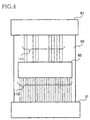
- FIG. 4 shows a developed appearance of one FPC 50.
- the driver IC 80 is represented by a broken line for convenience of description, and numerals in parentheses represents portions provided in the driver IC 80.
- FIG. 5 is an enlarged view of an area where the driver IC 80 is mounted on the FPC 50.
- the driver IC 80 has a rectangular shape, and includes a plurality of bumps 131, which are input electrodes and arranged along a side of the driver IC 80 closer to the board 81; a plurality of bumps 132, which are output electrodes and arranged along a side of the driver IC 80 closer to the actuator unit 21; and a plurality of bumps 133, which are test electrodes and arranged along the side of the driver IC 80 closer to the board 81 and used for operation test of the driver IC 80 during manufacturing.
- the bumps 131 through 133 are projecting electrodes formed with gold disposed on a surface of the driver IC 80 facing the FPC 50.
- the FPC 50 includes a plurality of lands 121 bonded to the bumps 131; a plurality of lands 122 bonded to the bumps 132; and a plurality of lands 123 bonded to the bumps 133.
- the lands 121 through 123 are given displacement plating with tin on a copper wiring pattern.
- the FPC 50 includes a wiring pattern 111 of which traces are bonded to the lands 121 for inputting the control signals, which are outputted from the board 81, in order to control the actuator unit 21, into the bumps 131; a wiring pattern 112 of traces that are bonded to the lands 122 for entering the drive signals, which are outputted from the driver IC 80, to drive the actuator unit 21, into the individual electrodes of the actuator unit 21; and a wiring pattern 113 of traces that are bonded to the lands 123 and does not input and output any signals to the bumps 133.
- the board 81 serially outputs about 3.3V control signals, generated to control the actuator unit 21, to the driver IC 80 via the wiring pattern 111, the lands 121, and the bumps 131, in this order.
- the driver IC 80 converts the control signals serially inputted from the board 81 into about 30V drive signals, and outputs the 30V drive signals to each of the individual electrodes (not shown) of the actuator unit 21 in parallel via the bumps 132, the lands 122, and the wiring pattern 112 in this order.
- the number of bumps 131 is less than that of bumps 132, and the number of traces of the wiring pattern 111 is thus less than that of the wiring pattern 112.
- the bumps 133 or test bumps have a certain degree of area, as they need contact with a probe when operation test of the driver IC 80 is performed.
- the area of the bump 133 is larger than that of the bump 131, 132.
- the area of the land 123 is also larger than that of the land 121, 122.
- the sum of the areas of the bumps 131, 133 arranged along the same side of the driver IC 80 is substantially the same as the sum of the areas of the bumps 132 arranged along the opposite side thereof.
- the sum of the areas of the lands 121, 123 arranged such as to face to the bumps 131, 133 is substantially the same as the sum of the areas of the lands 122 arranged facing to the bumps 132.
- the driver IC 80 In manufacturing process of the inkjet head 1, when the driver IC 80 is mounted on the FPC 50, the driver IC 80 is placed on the FPC 50 so that the bumps 131 to 133 face to the lands 121 to 123, and fixed by heat at a predetermined temperature. Thereby, gold on the bumps 131 to 133 is alloyed with tin on the lands 121 to 123, so that the bumps 131 to 133 are bonded to the lands 121 to 123.
- the FPC 50 is provided with the lands 123 to be bonded to the bumps 133, so that the sum of the areas of the bumps 131, 133 arranged on the same side is substantially the same as that of the bumps 132 arranged on the opposite side, and the sum of the areas of the lands 121, 123 arranged on the same side is substantially the same as that of the lands 122 arranged on the opposite side.
- the entire area where bumps and lands are bonded becomes wide, and the reliability to mount the driver IC 80 onto the FPC 50 can be increased.
- this structure distributes pressure generated when mounting evenly to each of the lands 121, 122, so that high reliable mounting can be performed.
- FIG. 6 is an enlarged view of an area where a driver IC 80A is mounted on a FPC 50A.
- the driver IC 80A is represented by a broken line and numerals in parentheses represents portions provided in the driver IC 80A.
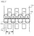
- FIG 7 is an enlarged view of an area indicated with a dash dot line shown in FIG 6.
- the driver IC 80A has a rectangular shape, and includes a plurality of bumps 131a, 131b, 131c, and 133, which are arranged along a side of the driver IC 80A closer to the board 81.
- the bumps 131a are electrodes to which control signals are inputted.
- the bumps 131b are ground electrodes, the bumps 131c are power electrodes, and the bumps 133 are test electrodes used for operation test of the driver IC 80A during manufacturing.
- the driver IC 80A also includes a plurality of bumps 132, 134, 135.
- the bumps 132 are arranged along a side of the driver IC 80A closer to the actuator unit 21.
- the bumps 132 are electrodes outputting drive signals.
- the bumps 134 are ground electrodes arranged such as to be parallel with a row of the bumps 131a, 131b, and 131c and a row of the bumps 132 therebetween.
- the bump 135 is a power electrode arranged between the row of the bumps 131a, 131b, and 131 c and the row of the bumps 134.
- the bumps 131a through 131c, 133, and 132 through 135 are projecting electrodes formed with gold disposed on a bottom surface of the driver IC 80A.
- the FPC 50A includes a plurality of lands 121a through 121c bonded to the bumps 131a through 131b; a plurality of lands 122 bonded to the bumps 132; a plurality of lands 123 bonded to the bumps 133; a plurality of lands 124 bonded to the bumps 134; and a land 125 bonded to the bump 135.
- the lands 121a through 121c and 122 through 125 are given displacement plating with tin on a copper wiring pattern.
- the FPC 50A includes a wiring pattern 111a which is connected to the lands 121a for inputting the control signals, which are outputted from the board 81, in order to control the actuator unit 21, into the bumps 131a; a wiring pattern 111b which is connected to the lands 121b for entering a ground potential common to the board 81, into the bumps 131b; a wiring pattern 111c, which is connected to the lands 121c for entering power into the bumps 131c; a wiring pattern 112, which is connected to the lands 122 for entering drive signals, which are outputted from the driver IC 80A, to drive the actuator unit 21, into the individual electrodes of the actuator unit 21; a wiring pattern 113, which is connected to the lands 123 and does not input and output any signals to the bumps 133; a ground pattern 114, which is connected to the lands 121b and the lands 124 for supplying a ground potential common to the board 81 to the bumps 131b and 134; and a power
- Each wiring pattern 111b, 111c extends to the corresponding lands 121b, 121c.
- Each wiring pattern 111b, 111c is separated into traces, forming a comb-like shape at its end near the lands 121b, 121c and outside the area where the driver IC 80A is disposed, and is connected to the corresponding lands 121b, 121c.
- This structure facilitates moving underfill material, which is a thermosetting resin to fix the driver IC 80A, into between the lands 121b and 121c.
- the bump 131b has a width greater than that of the land 121b.
- the land 121b has a width of 24 ⁇ m, and a pitch of the lands 121b and the bumps 131b is 48 ⁇ m. By making the pitch double the width of the land 121b, it can save space in the width direction and increase tolerances for positional deviations at mounting.
- the board 81 serially outputs about 3.3V control signals, generated to control the actuator unit 21, to the driver IC 80A via the wiring pattern 111a, the lands 121a, and the bumps 121b in this order.
- the driver IC 80A converts the control signals serially inputted from the board 81 into about 30V drive signals, and outputs the 30V drive signals to each of the individual electrodes (not shown) of the actuator unit 21 in parallel via the bumps 132, the lands 122, and the wiring patterns 112 in this order.
- the number of bumps 131a is less than that of bumps 132, and the number of traces of the wiring pattern 111a is thus less than that of the wiring pattern 112.
- the bumps 133 or test bumps have a certain degree of area, as they need contact with a probe when operation test of the driver IC 80A is performed.
- the area of the bump 133 is larger than that of the bump 131a, 132.
- the area of the land 123 is also larger than that of the land 121a, 122.
- the sum of the areas of the bumps 131a through 131c, 133 arranged along the same side of the driver IC 80A is substantially the same as the sum of the areas of the bumps 132 arranged along the opposite side thereof.
- the sum of the areas of the lands 121a through 121c, and 123 arranged such as to be bonded along the same side as the bumps 131a through 131c, 133 are arranged is substantially the same as the sum of the areas of the lands 122 arranged along the opposite side thereof.
- the ground pattern 114 is disposed such as to be parallel with a row of the lands 121a through 121c and 123 and a row of the lands 122 therebetween within an area where the driver IC 80A is placed.
- the ground pattern 114 extends linearly so as to pass the driver IC 80A in a direction perpendicular to two sides except for the side close to the board 81 and the side close to the actuator unit 21.
- the ground pattern 114 bends at right angles outside the area where the driver IC 80A is placed, and extends toward the board 81.
- the ground pattern 114 is connected to the lands 121b in the area where the driver IC 80A is placed.
- the power pattern 115 is disposed such as to be partially parallel between a row of the lands 121a through 121c, 123 and the ground pattern 114 within the area where the driver IC 80A is placed. In addition, the power pattern 115 is connected to the lands 121c within the area where the driver IC 80A is disposed.
- the lands 124, 125 which are disposed between the row of the lands 121a through 121c and 123 and the row of the lands 122, are bonded to the bumps 134, 135.
- the sum of the areas where the bumps and the lands are bonded is increased, thereby improving the entire strength to mount the driver IC onto the FPC, in addition to effects of the first embodiment.
- the ground pattern 114 and the power pattern 115 are connected to not only the lands 124, 125 but also the lands 121b, 121c, so that electrical resistances of the ground and the power supply source can be reduced.
- ground pattern 114 is placed such as to pass between the row of the lands 121a through 121c, 123 and the row of the lands 122 and cross over the driver IC 80A mounted.
- noise can be reduced in the wiring patterns 111a and 112.
- the power pattern 115 is disposed such as to be partially adjacent to and parallel with the ground pattern 114, so that the ground pattern 114 functions as a shield of the power pattern 115 and power noise can be reduced.
- the relationship between the power pattern 115 and the ground pattern 114 becomes equal to that they are connected to a capacitor, so that impedance of the power line can be reduced.
- the FPC 50 is structured to function as a power feed member in the inkjet head 1, however, it is not limited to such a structure.
- the FPC 50 may be an electrical circuit functioning as a member other than the power feed member.
- the FPC 50 is a thin printed circuit board and is made by employing technology called chip on film (COF) where bare chips are mounted on a polyimide film circuit board.
- COF chip on film
- it may be replaced with any kind of printed circuit board other than the FPC.
- the lands 123 are arranged in alignment with the lands 121 along the side of the driver IC 80 closer to the board 81, however, the lands 123 and the lands 121 may be arranged parallel to each other or both or one of the lands 123 and the lands 121 may be arranged in a staggered configuration.
- the driver IC 80 in which the control signals are inputted from the bumps 131 and the drive signals are outputted from the bumps 132, is mounted on the FPC 50.
- the invention is not limited to this structure.
- An element to be mounted may be structured so that any electrical signals can be inputted or outputted from all bumps arranged on all sides of the element.
- the test bumps 133 of the driver IC 80 are bonded to the lands 123.
- the FPC may be provided with lands to be bonded to bumps other than the test bumps, such that the sum of the area of the bumps arranged along a side of the driver IC may be substantially the same as that of the bumps arranged along the opposite side thereof, and the sum of areas of lands arranged such as to be bonded along the side may be substantially the same as that of lands arranged along the opposite side.
- the wiring pattern 113 is connected to the lands 123.
- the wiring pattern 113 may be omitted.
- the ground pattern 114 is placed such as to pass between the row of the lands 121a through 121c, 123 and the row of the lands 122 and cross over the driver IC 80A mounted.
- the ground pattern 114 may be disposed universally.
- the ground pattern 114 and the power pattern 115 may be omitted.
- a part of the power pattern 115 is disposed adjacently to and parallel to the ground pattern 114.
- the power pattern and the ground pattern may not be disposed adjacently to or parallel to each other.
Landscapes
- Structure Of Printed Boards (AREA)
- Wire Bonding (AREA)
- Particle Formation And Scattering Control In Inkjet Printers (AREA)
- Electric Connection Of Electric Components To Printed Circuits (AREA)
Applications Claiming Priority (2)
| Application Number | Priority Date | Filing Date | Title |
|---|---|---|---|
| JP2003424044A JP3772886B2 (ja) | 2003-12-22 | 2003-12-22 | プリント基板及びインクジェットヘッド |
| JP2003424044 | 2003-12-22 |
Publications (2)
| Publication Number | Publication Date |
|---|---|
| EP1548826A1 true EP1548826A1 (de) | 2005-06-29 |
| EP1548826B1 EP1548826B1 (de) | 2011-09-28 |
Family
ID=34544917
Family Applications (1)
| Application Number | Title | Priority Date | Filing Date |
|---|---|---|---|
| EP04257964A Expired - Lifetime EP1548826B1 (de) | 2003-12-22 | 2004-12-20 | Chipkontaktlayout |
Country Status (3)
| Country | Link |
|---|---|
| US (1) | US7271478B2 (de) |
| EP (1) | EP1548826B1 (de) |
| JP (1) | JP3772886B2 (de) |
Families Citing this family (7)
| Publication number | Priority date | Publication date | Assignee | Title |
|---|---|---|---|---|
| JP4822353B2 (ja) * | 2006-03-09 | 2011-11-24 | キヤノン株式会社 | 液体吐出ヘッド及びその製造方法 |
| JP5011871B2 (ja) * | 2006-07-28 | 2012-08-29 | 富士ゼロックス株式会社 | 液滴吐出ヘッド及び液滴吐出装置 |
| JP5556751B2 (ja) * | 2011-06-29 | 2014-07-23 | コニカミノルタ株式会社 | インクジェットヘッド |
| JP6033803B2 (ja) * | 2014-02-13 | 2016-11-30 | 株式会社東芝 | インクジェットヘッド |
| JP6183442B2 (ja) * | 2015-12-08 | 2017-08-23 | 株式会社リコー | 液滴吐出ヘッド及び液滴吐出装置 |
| JP6950425B2 (ja) * | 2017-09-29 | 2021-10-13 | ブラザー工業株式会社 | ヘッドユニット及び液体吐出装置 |
| US10960667B2 (en) * | 2018-03-19 | 2021-03-30 | Ricoh Company, Ltd. | Electronic device, liquid discharge head, liquid discharge device, liquid discharge apparatus, and electronic apparatus |
Citations (6)
| Publication number | Priority date | Publication date | Assignee | Title |
|---|---|---|---|---|
| JPS57117265A (en) | 1981-01-13 | 1982-07-21 | Nec Corp | Semiconductor device |
| US4411719A (en) | 1980-02-07 | 1983-10-25 | Westinghouse Electric Corp. | Apparatus and method for tape bonding and testing of integrated circuit chips |
| US5061988A (en) * | 1990-07-30 | 1991-10-29 | Mcdonnell Douglas Corporation | Integrated circuit chip interconnect |
| GB2344463A (en) | 1998-12-04 | 2000-06-07 | Nec Corp | Mounting a ball grid array device on a printed circuit board |
| US20020097299A1 (en) * | 2000-12-21 | 2002-07-25 | Makoto Terui | Liquid ejection print head |
| US20030128326A1 (en) * | 2001-12-28 | 2003-07-10 | Kabushiki Kaisha Advanced Display | Image display and manufacturing method thereof |
Family Cites Families (1)
| Publication number | Priority date | Publication date | Assignee | Title |
|---|---|---|---|---|
| JP2002353273A (ja) | 2001-05-22 | 2002-12-06 | Optrex Corp | 半導体装置の接続構造 |
-
2003
- 2003-12-22 JP JP2003424044A patent/JP3772886B2/ja not_active Expired - Fee Related
-
2004
- 2004-12-16 US US11/012,497 patent/US7271478B2/en not_active Expired - Lifetime
- 2004-12-20 EP EP04257964A patent/EP1548826B1/de not_active Expired - Lifetime
Patent Citations (6)
| Publication number | Priority date | Publication date | Assignee | Title |
|---|---|---|---|---|
| US4411719A (en) | 1980-02-07 | 1983-10-25 | Westinghouse Electric Corp. | Apparatus and method for tape bonding and testing of integrated circuit chips |
| JPS57117265A (en) | 1981-01-13 | 1982-07-21 | Nec Corp | Semiconductor device |
| US5061988A (en) * | 1990-07-30 | 1991-10-29 | Mcdonnell Douglas Corporation | Integrated circuit chip interconnect |
| GB2344463A (en) | 1998-12-04 | 2000-06-07 | Nec Corp | Mounting a ball grid array device on a printed circuit board |
| US20020097299A1 (en) * | 2000-12-21 | 2002-07-25 | Makoto Terui | Liquid ejection print head |
| US20030128326A1 (en) * | 2001-12-28 | 2003-07-10 | Kabushiki Kaisha Advanced Display | Image display and manufacturing method thereof |
Non-Patent Citations (1)
| Title |
|---|
| PATENT ABSTRACTS OF JAPAN vol. 006, no. 211 (E - 137) 23 October 1982 (1982-10-23) * |
Also Published As
| Publication number | Publication date |
|---|---|
| JP3772886B2 (ja) | 2006-05-10 |
| US20050133898A1 (en) | 2005-06-23 |
| US7271478B2 (en) | 2007-09-18 |
| EP1548826B1 (de) | 2011-09-28 |
| JP2005183752A (ja) | 2005-07-07 |
Similar Documents
| Publication | Publication Date | Title |
|---|---|---|
| US8469493B2 (en) | Flexible wiring member, liquid droplet jetting head, and method for connecting flexible wiring member and device | |
| US7585060B2 (en) | Liquid ejecting head and liquid ejecting apparatus | |
| US9944076B2 (en) | Liquid discharge head and liquid discharge apparatus | |
| US10618281B2 (en) | Ink jet head and ink jet printer | |
| JP7074232B2 (ja) | アクチュエータ装置、及び、液体吐出装置 | |
| US10611148B2 (en) | Ink jet head and ink jet printer | |
| US10814616B2 (en) | Inkjet head, inkjet printer, and manufacturing method for inkjet head | |
| EP2769846B1 (de) | Flüssigkeitsausstoßvorrichtung und Verbindungsverfahren für flexible Leiterplatte | |
| US7478896B2 (en) | Ink jet head | |
| JP2017124540A (ja) | 配線基板、memsデバイス及び液体噴射ヘッド | |
| US7271478B2 (en) | Printed circuit board and inkjet head | |
| CN109720091B (zh) | 头单元 | |
| CN100446978C (zh) | 软性印刷电路板的结构 | |
| US10639895B2 (en) | Liquid ejecting head and liquid ejecting apparatus | |
| JP5057043B2 (ja) | 電子部品が搭載されたフレキシブル基板及びそれを備えた記録装置 | |
| JP7087325B2 (ja) | 電子デバイス | |
| JP7006062B2 (ja) | 配線基板、配線部材、液体吐出ヘッド、液体吐出ユニット、液体を吐出する装置 | |
| US20080128159A1 (en) | Method for manufacturing a printed circuit board that mounts an integrated circuit device thereon and the printed circuit board | |
| CN110962457B (zh) | 液体喷射头 | |
| JP7147412B2 (ja) | 液体吐出装置及び配線部材 | |
| JP7757121B2 (ja) | 液体吐出ヘッドおよびその製造方法 | |
| JP2022095995A (ja) | アクチュエータ装置、及び、液体吐出装置 | |
| JP2019047073A (ja) | フレキシブル部材、配線部材、液体吐出ヘッド、液体吐出ユニット、液体を吐出する装置、電子機器 | |
| JP2008238413A (ja) | 液体噴射ヘッド用配線部材、及び、液体噴射ヘッド | |
| US20250229532A1 (en) | Flexible board, liquid jet head, and liquid jet recording apparatus |
Legal Events
| Date | Code | Title | Description |
|---|---|---|---|
| PUAI | Public reference made under article 153(3) epc to a published international application that has entered the european phase |
Free format text: ORIGINAL CODE: 0009012 |
|
| AK | Designated contracting states |
Kind code of ref document: A1 Designated state(s): AT BE BG CH CY CZ DE DK EE ES FI FR GB GR HU IE IS IT LI LT LU MC NL PL PT RO SE SI SK TR |
|
| AX | Request for extension of the european patent |
Extension state: AL BA HR LV MK YU |
|
| 17P | Request for examination filed |
Effective date: 20050831 |
|
| AKX | Designation fees paid |
Designated state(s): DE FR GB |
|
| 17Q | First examination report despatched |
Effective date: 20090812 |
|
| GRAP | Despatch of communication of intention to grant a patent |
Free format text: ORIGINAL CODE: EPIDOSNIGR1 |
|
| GRAS | Grant fee paid |
Free format text: ORIGINAL CODE: EPIDOSNIGR3 |
|
| GRAA | (expected) grant |
Free format text: ORIGINAL CODE: 0009210 |
|
| AK | Designated contracting states |
Kind code of ref document: B1 Designated state(s): DE FR GB |
|
| REG | Reference to a national code |
Ref country code: GB Ref legal event code: FG4D |
|
| REG | Reference to a national code |
Ref country code: DE Ref legal event code: R082 Ref document number: 602004034525 Country of ref document: DE Representative=s name: PRUEFER & PARTNER GBR, DE Ref country code: DE Ref legal event code: R082 Ref document number: 602004034525 Country of ref document: DE Representative=s name: PRUEFER & PARTNER MBB PATENTANWAELTE RECHTSANW, DE |
|
| REG | Reference to a national code |
Ref country code: DE Ref legal event code: R096 Ref document number: 602004034525 Country of ref document: DE Effective date: 20111222 |
|
| PLBE | No opposition filed within time limit |
Free format text: ORIGINAL CODE: 0009261 |
|
| STAA | Information on the status of an ep patent application or granted ep patent |
Free format text: STATUS: NO OPPOSITION FILED WITHIN TIME LIMIT |
|
| 26N | No opposition filed |
Effective date: 20120629 |
|
| REG | Reference to a national code |
Ref country code: DE Ref legal event code: R097 Ref document number: 602004034525 Country of ref document: DE Effective date: 20120629 |
|
| REG | Reference to a national code |
Ref country code: FR Ref legal event code: PLFP Year of fee payment: 12 |
|
| REG | Reference to a national code |
Ref country code: FR Ref legal event code: PLFP Year of fee payment: 13 |
|
| REG | Reference to a national code |
Ref country code: FR Ref legal event code: PLFP Year of fee payment: 14 |
|
| PGFP | Annual fee paid to national office [announced via postgrant information from national office to epo] |
Ref country code: DE Payment date: 20191114 Year of fee payment: 16 |
|
| PGFP | Annual fee paid to national office [announced via postgrant information from national office to epo] |
Ref country code: FR Payment date: 20191122 Year of fee payment: 16 |
|
| PGFP | Annual fee paid to national office [announced via postgrant information from national office to epo] |
Ref country code: GB Payment date: 20191126 Year of fee payment: 16 |
|
| REG | Reference to a national code |
Ref country code: DE Ref legal event code: R119 Ref document number: 602004034525 Country of ref document: DE |
|
| GBPC | Gb: european patent ceased through non-payment of renewal fee |
Effective date: 20201220 |
|
| PG25 | Lapsed in a contracting state [announced via postgrant information from national office to epo] |
Ref country code: FR Free format text: LAPSE BECAUSE OF NON-PAYMENT OF DUE FEES Effective date: 20201231 |
|
| PG25 | Lapsed in a contracting state [announced via postgrant information from national office to epo] |
Ref country code: GB Free format text: LAPSE BECAUSE OF NON-PAYMENT OF DUE FEES Effective date: 20201220 Ref country code: DE Free format text: LAPSE BECAUSE OF NON-PAYMENT OF DUE FEES Effective date: 20210701 |