EP1547148B1 - Plan d'integration d'espacement dans la technologie mram - Google Patents
Plan d'integration d'espacement dans la technologie mram Download PDFInfo
- Publication number
- EP1547148B1 EP1547148B1 EP03779791A EP03779791A EP1547148B1 EP 1547148 B1 EP1547148 B1 EP 1547148B1 EP 03779791 A EP03779791 A EP 03779791A EP 03779791 A EP03779791 A EP 03779791A EP 1547148 B1 EP1547148 B1 EP 1547148B1
- Authority
- EP
- European Patent Office
- Prior art keywords
- layer
- free layer
- tunnel barrier
- sidewalls
- pinned
- Prior art date
- Legal status (The legal status is an assumption and is not a legal conclusion. Google has not performed a legal analysis and makes no representation as to the accuracy of the status listed.)
- Expired - Lifetime
Links
- 125000006850 spacer group Chemical group 0.000 title description 12
- 230000010354 integration Effects 0.000 title 1
- 230000004888 barrier function Effects 0.000 claims description 30
- 238000000034 method Methods 0.000 claims description 23
- 230000005291 magnetic effect Effects 0.000 claims description 21
- 239000000463 material Substances 0.000 claims description 14
- 230000008569 process Effects 0.000 claims description 14
- 238000005530 etching Methods 0.000 claims description 13
- 238000000151 deposition Methods 0.000 claims description 9
- 238000000059 patterning Methods 0.000 claims description 9
- 239000002131 composite material Substances 0.000 claims description 7
- 238000004519 manufacturing process Methods 0.000 claims description 7
- 238000002161 passivation Methods 0.000 claims description 5
- 230000008021 deposition Effects 0.000 claims description 4
- 239000000696 magnetic material Substances 0.000 claims description 4
- 230000001681 protective effect Effects 0.000 claims description 4
- 239000004020 conductor Substances 0.000 claims description 2
- 239000010410 layer Substances 0.000 description 95
- 229910052751 metal Inorganic materials 0.000 description 14
- 239000002184 metal Substances 0.000 description 14
- 230000015572 biosynthetic process Effects 0.000 description 11
- RYGMFSIKBFXOCR-UHFFFAOYSA-N Copper Chemical compound [Cu] RYGMFSIKBFXOCR-UHFFFAOYSA-N 0.000 description 7
- 229910052802 copper Inorganic materials 0.000 description 7
- 239000010949 copper Substances 0.000 description 7
- 230000005294 ferromagnetic effect Effects 0.000 description 6
- 229910003321 CoFe Inorganic materials 0.000 description 5
- 238000012545 processing Methods 0.000 description 4
- 239000000758 substrate Substances 0.000 description 4
- PNEYBMLMFCGWSK-UHFFFAOYSA-N aluminium oxide Inorganic materials [O-2].[O-2].[O-2].[Al+3].[Al+3] PNEYBMLMFCGWSK-UHFFFAOYSA-N 0.000 description 3
- 238000013461 design Methods 0.000 description 3
- 229910001030 Iron–nickel alloy Inorganic materials 0.000 description 2
- ATJFFYVFTNAWJD-UHFFFAOYSA-N Tin Chemical compound [Sn] ATJFFYVFTNAWJD-UHFFFAOYSA-N 0.000 description 2
- 229910045601 alloy Inorganic materials 0.000 description 2
- 239000000956 alloy Substances 0.000 description 2
- 229910052782 aluminium Inorganic materials 0.000 description 2
- XAGFODPZIPBFFR-UHFFFAOYSA-N aluminium Chemical compound [Al] XAGFODPZIPBFFR-UHFFFAOYSA-N 0.000 description 2
- 230000008901 benefit Effects 0.000 description 2
- 239000003989 dielectric material Substances 0.000 description 2
- 230000006872 improvement Effects 0.000 description 2
- 230000005381 magnetic domain Effects 0.000 description 2
- 150000004767 nitrides Chemical class 0.000 description 2
- 229910000889 permalloy Inorganic materials 0.000 description 2
- 230000009467 reduction Effects 0.000 description 2
- 229910052710 silicon Inorganic materials 0.000 description 2
- 238000004544 sputter deposition Methods 0.000 description 2
- 238000003860 storage Methods 0.000 description 2
- ZAMOUSCENKQFHK-UHFFFAOYSA-N Chlorine atom Chemical compound [Cl] ZAMOUSCENKQFHK-UHFFFAOYSA-N 0.000 description 1
- YCKRFDGAMUMZLT-UHFFFAOYSA-N Fluorine atom Chemical compound [F] YCKRFDGAMUMZLT-UHFFFAOYSA-N 0.000 description 1
- 229910001218 Gallium arsenide Inorganic materials 0.000 description 1
- 229910019041 PtMn Inorganic materials 0.000 description 1
- 229910000577 Silicon-germanium Inorganic materials 0.000 description 1
- 238000013459 approach Methods 0.000 description 1
- QVGXLLKOCUKJST-UHFFFAOYSA-N atomic oxygen Chemical compound [O] QVGXLLKOCUKJST-UHFFFAOYSA-N 0.000 description 1
- 229910052801 chlorine Inorganic materials 0.000 description 1
- 239000000460 chlorine Substances 0.000 description 1
- 238000010276 construction Methods 0.000 description 1
- 230000007547 defect Effects 0.000 description 1
- 230000002950 deficient Effects 0.000 description 1
- 238000001312 dry etching Methods 0.000 description 1
- 239000003302 ferromagnetic material Substances 0.000 description 1
- 229910052731 fluorine Inorganic materials 0.000 description 1
- 239000011737 fluorine Substances 0.000 description 1
- 230000004907 flux Effects 0.000 description 1
- 230000006870 function Effects 0.000 description 1
- 239000011521 glass Substances 0.000 description 1
- 239000007943 implant Substances 0.000 description 1
- 239000011229 interlayer Substances 0.000 description 1
- 150000002500 ions Chemical class 0.000 description 1
- 238000001459 lithography Methods 0.000 description 1
- 238000005259 measurement Methods 0.000 description 1
- 230000005055 memory storage Effects 0.000 description 1
- 239000000203 mixture Substances 0.000 description 1
- 238000012986 modification Methods 0.000 description 1
- 230000004048 modification Effects 0.000 description 1
- 239000001301 oxygen Substances 0.000 description 1
- 229910052760 oxygen Inorganic materials 0.000 description 1
- 238000001637 plasma atomic emission spectroscopy Methods 0.000 description 1
- 238000001020 plasma etching Methods 0.000 description 1
- 238000005498 polishing Methods 0.000 description 1
- 238000004886 process control Methods 0.000 description 1
- 230000000284 resting effect Effects 0.000 description 1
- 239000004065 semiconductor Substances 0.000 description 1
- 239000010703 silicon Substances 0.000 description 1
- 239000002356 single layer Substances 0.000 description 1
- 230000003746 surface roughness Effects 0.000 description 1
- WFKWXMTUELFFGS-UHFFFAOYSA-N tungsten Chemical compound [W] WFKWXMTUELFFGS-UHFFFAOYSA-N 0.000 description 1
- 229910052721 tungsten Inorganic materials 0.000 description 1
- 239000010937 tungsten Substances 0.000 description 1
- 230000005641 tunneling Effects 0.000 description 1
Images
Classifications
-
- H—ELECTRICITY
- H10—SEMICONDUCTOR DEVICES; ELECTRIC SOLID-STATE DEVICES NOT OTHERWISE PROVIDED FOR
- H10N—ELECTRIC SOLID-STATE DEVICES NOT OTHERWISE PROVIDED FOR
- H10N50/00—Galvanomagnetic devices
- H10N50/01—Manufacture or treatment
Definitions
- the field of the invention is that of magnetic random access memory (MRAM), in particular the design of an array device to improve the fabrication process yield.
- MRAM magnetic random access memory
- Magneto resistive tunnel junction devices used in a random access memory array are formed by depositing a blanket metal stack comprised of a pinned magnetic layer, a tunnel barrier layer and a free magnetic layer, such as that described in U.S. Patent 5,650,958 .
- Several process steps are made to define the magneto resistive tunnel junction device that comprises the storage element of a memory array cell.
- the bit is written by orienting the net magnetic moment of the free layer parallel or antiparallel to the pinned layer magnetic moment.
- the bit is read by sensing the amount of current tunneling through the barrier junction from the free layer to the pinned layer.
- the two bit states correspond to the junction resistance of the parallel and antiparallel orientations of the freelayer relative to the pinned layer.
- the operation of the tunnel barrier device is more complicated than the simple model described above.
- variations in the orientation of the freelayer magnetic moment in nominally the same state, introduce additional noise that the sense amplifiers must discern.
- Defects generated in the sidewalls during the fabrication process can impart the tendency of the magnetic domains to orient in offaxis orientations.
- the reduction of these variations by process improvements is desirable as this results in larger signal margins in a product array. Additional performance is obtained by increasing the signal margin.
- the invention relates to a method for fabricating a magnetoresistive tunnel junction device for use in a memory cell, in which a set of sidewalls protects exposed edges of sensitive layers during etching.
- a feature of the invention is the passivation of the external edges of exposed ferromagnetic layers.
- Another feature of the invention is the formation of sidewalls along the edges of a temporary mandrel that supports the sidewalls and provides a contact into the cell.
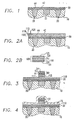
- Figures 1 - 8 show in partially pictorial, partially schematic form, cross sections of portions of a magneto resistive tunnel junction device, illustrating the process sequence made to define the invention described herein.
- Fig. 1 there is shown in cross section a portion of an integrated circuit that is being prepared for construction of an MRAM cell, part of a memory array.
- Substrate 10 illustratively silicon, has been prepared by forming wells, threshold implants, etc. as part of standard integrated circuit processing up to at least the first level of interconnect-dielectric deposition.
- conductive interconnection members 20 and 22 have been formed in substrate 10 by damascene processing.
- a dielectric layer, e.g. oxide 30 has been put down and a via 44 and local device wiring interconnect 42 have been formed.
- they are TaN, but any other conductive material compatible with standard processing, e.g. copper, tungsten or aluminum, could be used.
- the top surface of the local device wiring interconnect 42 has been planarized by chemical-mechanical polishing (CMP) as is standard in the field. This surface is critical to optimal MRAM device performance and care must be made to mitigate surface roughness.
- CMP chemical-mechanical polishing
- a blanket stack of magnetic material denoted generally by the numeral 100, has been deposited to form the basis for the array of MRAM devices.
- Stack 100 shows the generic three layers of a magnetic memory cell - the pinned layer (110), the tunnel barrier layer (115) and the free layer (120).
- Each of these layers may be a composite of several sublayers, as shown in U.S. Patent 5,650,958 , assigned to the assignee hereof.
- layer 110 in the Figures represents schematically the ferromagnetic pinned layer of the cell, plus additional layers such as a buffer layer 101 on the bottom of layer 110 (e.g. TaN), and a pinning layer 105 (e.g.
- a dielectric tunnel barrier layer 115 (e.g. alumina) separates the two magnetic conductive layers.
- the free layer 120 may also include a cap layer 125. Free layer 120 may be, for example, a layer of permalloy (NiFe).
- the tunnel barrier layer 115 is usually alumina (A1203) but any other material providing tunnel barrier characteristics may also be used.
- the pinned layer 110 may be a single layer of CoFe or a composite of CoFe/Ru layers, for example.
- Other ferromagnetic materials may be used in place of those described herein to perform the same device function.
- other alloy compositions of CoFe are employed as pinned ferromagnetic layers and also alloys of CoFe alloyed with B, Si, for example are used for the freelayer 120.
- An advantageous feature of the invention is a temporary mandrel that enables the formation of a self-aligned vertical electrode for contact to the free layer of the device.
- the disposable mandrel is used to support an etch mask in the form of a spacer along the sidewall of the mandrel and the etched freelayer to the tunnel barrier interface.
- An advantage of this method is that the height if the mandrel can be substantial, which allows the formation of a sufficient etch mask with a thin sidewall. This feature is not required, however, for the sidewall spacer formation and a more traditional approach using a conductive hardmask, such as TiN or TaN, can also be used.
- Another advantage of the invention is the formation of a passivation layer, which reduces pinning of magnetic domains in the free layer from imperfections in the device sidewall. Ideally, this reduction of pinning allows the freelayer to switch into two distinct predefined states thereby providing improved signal-to-noise conditions for the array sense amplifier. It is necessary for such signal improvement that the material surrounding the mandrel be deposited directly onto the exposed surface of the junction which is the case for spacer deposition according to the invention. Utilizing the sidewall spacer to provide junction passivation permits this additional requirement to be satisfied independent of the choice of interlevel dielectric material, e.g. alumina or nitride.
- the junction protection provided by the sidewall spacer of the invention is particularly useful for the formation of a cross point memory array directly on copper wiring.
- This cell architecture requires the fabrication of the magneto- resistive device directly on the interconnect wiring beneath the device. The fabrication of this device requires etching completely through the magnetic metal stack, thereby exposing the copper metal interconnect. The sputter yield of copper is relatively large, which increases the rate of redeposited metal during etch thereby increasing the probability of junction shorting. By providing a dielectric spacer along the sidewall of the tunnel junction, the potential for sidewall shorting is substantially reduced.
- the bit stored in the cell is read by flowing current through the tunnel barrier of the device from a contact shown in later figures through stack 100 and then through interconnections 42, 44 and 20.
- the bit is written by flowing a current horizontally in the figure through adjacent interconnect wiring below and above the device, e.g. wiring interconnect 22 and one of the layers in the stack, also as is conventional for the magneto resistive device design illustrated in the figures.
- the so-called offset cell architecture features a magneto resistive device wired in series with a transistor to provide increased signal and faster access time.
- the crosspoint device design wires the magneto resistive device between adjacent wiring levels in an integrated circuit which results in a common bottom contact for the read and write operations.
- an illustrative cell in the array is patterned by first forming a mandrel 60 on the stack of magnetic materials, the mandrel comprising a spinon glass 61 (SOG,) a dielectric mask bottom layer of nitride 62 and an upper layer of oxide 64.
- Alternative hardmask materials such as TiN or TaN, may similarly be used in the patterning process, as those skilled in the art are aware.
- the mandrel hardmask 60 for the subsequent metal etch process is formed and the magnetic layers are etched using the mandrel as a mask.
- the ferromagnetic free layer 120 is etched, to define cell layers 122 and 117, respectively, shown in figure 3 .
- the freelayer etch process etch through the tunnel barrier layer 115 and pinned layer 110 stopping in the pinning layer that is a lower level in the composite layer 110.
- the etch proceeds through TaN cap layer 125 and freelayer 120 and stops on the barrier layer 115, using, for example, a chlorine-based reactive etch chemistry masked by the mandrel structure 60 or alternative conductive hardmask.
- the embodiment according to the invention employs a similar etch chemistry to etch the freelayer 120, barrier layer 115 and pinned layer 110, stopping in the pinning layer 105 that is the next level in the composite layer 110.
- the etch chamber process conditions are adjusted together with plasma emission spectroscopy measurements to facilitate an endpoint signal for an etch stop on the particular layer.
- the freelayer 120 and barrier layer 115 are about 4, and 1 nanometers thick, respectively, requiring etch selectivity control to achieve the stop on the barrier in addition to the previous process controls.
- the result is shown in Fig. 3 , with the upper layers of the magnetic stack patterned.
- An important problem addressed by the invention is that of current leakage along these stack edges and also direct shorting of the barrier layer 115, which are caused in prior art fabrication by sputtering of metal from the pinned layer 110 or pinning layer.
- the sidewall redeposition is more of a problem with the crosspoint device structure since copper, which has a high sputter yield, is exposed during the metal stack etch.
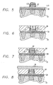
- a blanket dielectric layer 72 such as SiN, A1203, or other material that can be deposited at a temperature compatible with back end processing and can be removed with a directional etch, is conformally deposited on the wafer as shown in Fig. 4 .
- the properties of the material are designed to minimize the leakage current along the device sidewalls, in addition to optimizing device characteristics such as reliability.
- This layer is then etched with a suitable fluorine-based dielectric etch chemistry available in commercial etch tooling to form the passivation sidewall spacer 82 shown in Fig. 5 .
- layer 110 is etched outside the sidewall spacer 82, leaving the structure shown in Fig. 6 , with the cell stack having sidewall spacer 82 that rests on horizontal projections of layer 112, formed from the composite pinned layer.
- the stack material at the edges of the free and tunnel layers is passivated by dielectric 72 and/or the material of sidewalls 82. Any sputtering from the exposed surfaces of pinned ferromagnetic layer 110, the pinning layer 105, the buffer layer 101, or metal 42 will not deposit on the exposed edges of layers 122 and 117 because of the protective effect of sidewalls 82.
- the mandrel hardmask structure 60 with the sidewall spacer 82 formed around the perimeter of the device, illustrated in Fig. 6 is then used to complete the metal etch process for the particular device.
- the additional etch process involves etching through pinned layer 110 stopping in the pinning layer. This results in formation of the shaped layers 122, 117 and 112, shown also in Fig. 6 . It may also be desirable to etch through the pinning layer 105, stopping on the TaN buffer layer 101 at the bottom of composite layer 110. Another option is to etch through the pinned layer 110, the pinning layer 105 and the TaN buffer layer 101.
- a relatively thick dielectric layer 86 is deposited over the entire structure, including the space between cells, to a depth sufficient to allow for formation of a contact. Excess amounts of layer 86 are removed to expose the top surface of mandrel 60. The mandrel is removed in a conventional dielectric etch, leaving an aperture 66 having layer 122 (the top layer of the magnetic stack 100) on its bottom, that will be filled with an electrode for the cell. Illustratively, the etch is made using a oxygen based plasma strip process, with substantial selectivity to the cap layer material 122. As shown in Fig. 7 , a layer of copper is deposited to form electrode 92.
- final dielectric 86 is SiLK(TM) or other low-k material for a high-performance integrated circuit.
- Other conventional interlayer dielectric materials could be used, as well, especially if high switching speed is not required in the particular application.
- FIG. 8 A final structure is shown in Fig. 8 , in which a second metal layer 95 has been deposited and planarized, making contact with electrode 92.
- a second metal layer 95 has been deposited and planarized, making contact with electrode 92.
- the substrate may be SiGe, GaAs or any other semiconductor.
- the cell has been shown as resting on the substrate, but may be formed at a higher level in the total integrated circuit structure.
- the electrical connections are preferably copper in a low-k dielectric, but may be aluminum in oxide or any other combination meeting the electrical requirements of the chip being fabricated.
- the chip may be a magnetic random access memory or may be a logic chip containing an array of memory cells in it.
Landscapes
- Engineering & Computer Science (AREA)
- Manufacturing & Machinery (AREA)
- Mram Or Spin Memory Techniques (AREA)
- Hall/Mr Elements (AREA)
- Semiconductor Memories (AREA)
Claims (8)
- Procédé pour faire au moins une cellule de mémoire magnétique comprenant les stades de :dépôt d'un empilage (100) de mémoire de matériaux magnétiques contenant une couche (110) de connexion, une couche (120) libre et une couche (115) barrière de tunnel disposée entre la couche (110) de connexion et la couche (115) barrière de tunnel ;formation d'un masque (60) dur résistant à une attaque chimique et définissant au moins une zone de cellule de l'empilage (100) de mémoire ;structuration d'au moins une couche de l'empilage de mémoire par attaque à l'extérieur du masque dur en laissant une surface verticale mise à nu de cette au moins une couche ;dépôt d'un diélectrique (72) conforme sur le masque (60) dur et attaque du diélectrique (72) conforme d'une manière directionnelle pour former des parois (82) latérales de protection s'étendant sur des bords de la couche (120) libre et de la couche (115) barrière de tunnel mise à nu par le stade d'attaque, en formant ainsi des parois (82) latérales de protection autour de l'empilage (100) de mémoire recouvrant la surface verticale mise à nu ; etstructuration de couches restantes de l'empilage (100) de mémoire, la surface verticale mise à nu étant protégée pendant le stade de structuration des couches restantes de l'empilage (100) de mémoire.
- Procédé suivant la revendication 1, dans lequel la couche (120) libre est la couche supérieure de l'empilage (100) de mémoire et le stade de structuration comprend attaquer dans la couche (120) libre et arrêter l'attaque sur la couche (115) barrière de tunnel.
- Procédé suivant la revendication 1, dans lequel la couche (120) libre est la couche supérieure de l'empilage (100) de mémoire et le stade de structuration comprend attaquer dans la couche (120) libre et dans la couche (115) barrière de tunnel et arrêter l'attaque sur la couche (110) de connexion.
- Procédé suivant la revendication 1, dans lequel la couche (120) libre est la couche supérieure de l'empilage (100) de mémoire et le stade de structuration comprend attaquer dans la couche (120) libre et dans la couche (115) barrière de tunnel et arrêter l'attaque dans une couche de contact, qui est une sous-couche d'une couche composite de connexion.
- Procédé suivant l'une quelconque des revendications 1 à 4, comprenant, en outre, un stade d'attaque dans la couche (110) de connexion à l'extérieur des parois latérales, une couche de connexion de la cellule de mémoire étant formée et s'étendant en dessous des parois latérales et étant auto-alignée avec la couche (120) libre et avec la couche (115) barrière de tunnel et des bords mis à nu de la couche (120) libre et de la couche (115) barrière de tunnel étant protégés du dépôt de matière pulvérisée cathodiquement pendant l'opération d'attaque.
- Procédé suivant la revendication 5, comprenant, en outre, un stade de dépôt du diélectrique (72) autour du masque (60) dur, en enfermant ainsi les parois latérales jusqu'à un niveau supérieur du masque (60) dur ;
d'élimination du masque (60) dur, de mise à nu d'une couche supérieure de l'empilage (100) magnétique au bas d'une ouverture (66) du masque dur ; et
de dépôt d'un matériau (92) conducteur dans l'ouverture du masque dur, en formant ainsi un contact de cellule. - Cellule de mémoire magnétique comprenant une couche (120) libre, une couche (110) de connexion et une couche (115) barrière de tunnel disposée sur un axe vertical entre la couche (120) libre et la couche (110) de connexion ;
une électrode (42) inférieure de cellule disposée verticalement en dessous de la couche (110) de connexion et en contact électrique avec elle ;
une électrode (122) supérieure de cellule disposée verticalement sur la couche (120) libre et en contact électrique avec elle ;
un jeu de parois (82) latérales de diélectrique enfermant l'électrode de cellule et s'étendant verticalement le long d'au moins un bord mis à nu de la couche (120) libre, les parois (82) latérales de diélectrique étant disposées verticalement au-dessus d'un prolongement de la couche (110) de connexion, qui s'étend horizontalement au-delà de la couche (120) libre, les parois (82) latérales de diélectrique s'étendant verticalement dans une couche de contact, qui est une sous-couche de la couche (110) de connexion, la couche de connexion ayant un bord mis à nu aligné verticalement avec le bord mis à nu de la couche (120) libre. - Cellule de mémoire magnétique suivant la revendication 7, dans lequel les parois (82) latérales de diélectrique sont en un matériau de passivation, les parois (82) latérales de diélectrique passivant le bord mis à nu de la couche (120) libre.
Applications Claiming Priority (3)
| Application Number | Priority Date | Filing Date | Title |
|---|---|---|---|
| US10/261,709 US6985384B2 (en) | 2002-10-01 | 2002-10-01 | Spacer integration scheme in MRAM technology |
| US261709 | 2002-10-01 | ||
| PCT/EP2003/010678 WO2004032144A2 (fr) | 2002-10-01 | 2003-09-24 | Plan d'integration d'espacement dans la technologie mram |
Publications (2)
| Publication Number | Publication Date |
|---|---|
| EP1547148A2 EP1547148A2 (fr) | 2005-06-29 |
| EP1547148B1 true EP1547148B1 (fr) | 2012-11-28 |
Family
ID=32030041
Family Applications (1)
| Application Number | Title | Priority Date | Filing Date |
|---|---|---|---|
| EP03779791A Expired - Lifetime EP1547148B1 (fr) | 2002-10-01 | 2003-09-24 | Plan d'integration d'espacement dans la technologie mram |
Country Status (4)
| Country | Link |
|---|---|
| US (2) | US6985384B2 (fr) |
| EP (1) | EP1547148B1 (fr) |
| TW (1) | TWI243430B (fr) |
| WO (1) | WO2004032144A2 (fr) |
Families Citing this family (44)
| Publication number | Priority date | Publication date | Assignee | Title |
|---|---|---|---|---|
| US7220427B2 (en) * | 1998-07-08 | 2007-05-22 | Oryxe | Mixture for transdermal delivery of low and high molecular weight compounds |
| US6943039B2 (en) * | 2003-02-11 | 2005-09-13 | Applied Materials Inc. | Method of etching ferroelectric layers |
| JP4008857B2 (ja) * | 2003-03-24 | 2007-11-14 | 株式会社東芝 | 半導体記憶装置及びその製造方法 |
| US6911156B2 (en) * | 2003-04-16 | 2005-06-28 | Freescale Semiconductor, Inc. | Methods for fabricating MRAM device structures |
| US20060138576A1 (en) * | 2003-06-24 | 2006-06-29 | Galdis Michael C | Self-aligned conductive lines for fet-based magnetic random access memory devices and method of forming the same |
| US20050090119A1 (en) * | 2003-10-24 | 2005-04-28 | Heon Lee | Magnetic tunnel junction device with dual-damascene conductor and dielectric spacer |
| US20050090111A1 (en) * | 2003-10-24 | 2005-04-28 | Heon Lee | Magnetic tunnel junction device with etch stop layer and dielectric spacer |
| KR100561859B1 (ko) * | 2004-01-16 | 2006-03-16 | 삼성전자주식회사 | 컨택홀이 없는 나노 크기의 자기터널접합 셀 형성 방법 |
| JP4074281B2 (ja) * | 2004-09-14 | 2008-04-09 | 株式会社東芝 | 磁気ランダムアクセスメモリ |
| US7350284B2 (en) * | 2004-10-29 | 2008-04-01 | Hitachi Global Storage Technologies Netherlands B.V. | Methods of making a current-perpendicular-to-the-planes (CPP) type sensor by ion milling to the spacer layer using a mask without undercuts |
| TWI266413B (en) * | 2004-11-09 | 2006-11-11 | Ind Tech Res Inst | Magnetic random access memory with lower bit line current and manufacture method thereof |
| DE102004054558A1 (de) * | 2004-11-11 | 2006-05-24 | Infineon Technologies Ag | Verfahren zur Herstellung einer resistiv schaltenden Speicherzelle, hergestellte Speicherzelle sowie daraus aufgebautes Speicherbauelement |
| US7105903B2 (en) | 2004-11-18 | 2006-09-12 | Freescale Semiconductor, Inc. | Methods and structures for electrical communication with an overlying electrode for a semiconductor element |
| JP2006179701A (ja) * | 2004-12-22 | 2006-07-06 | Toshiba Corp | 磁気ランダムアクセスメモリ |
| US7880249B2 (en) | 2005-11-30 | 2011-02-01 | Magic Technologies, Inc. | Spacer structure in MRAM cell and method of its fabrication |
| US8450119B2 (en) * | 2006-03-17 | 2013-05-28 | Magic Technologies, Inc. | Magnetic tunnel junction patterning using Ta/TaN as hard mask |
| US7442647B1 (en) * | 2008-03-05 | 2008-10-28 | International Business Machines Corporation | Structure and method for formation of cladded interconnects for MRAMs |
| CN102246327B (zh) * | 2008-12-10 | 2013-11-27 | 株式会社日立制作所 | 磁阻效应元件、使用其的磁存储单元及磁随机存取存储器 |
| US8685756B2 (en) | 2011-09-30 | 2014-04-01 | Everspin Technologies, Inc. | Method for manufacturing and magnetic devices having double tunnel barriers |
| US9793467B2 (en) | 2011-12-20 | 2017-10-17 | Intel Corporation | Method for reducing size and center positioning of magnetic memory element contacts |
| US8883520B2 (en) | 2012-06-22 | 2014-11-11 | Avalanche Technology, Inc. | Redeposition control in MRAM fabrication process |
| US8747680B1 (en) * | 2012-08-14 | 2014-06-10 | Everspin Technologies, Inc. | Method of manufacturing a magnetoresistive-based device |
| US8790935B1 (en) * | 2012-10-22 | 2014-07-29 | Everspin Technologies, Inc. | Method of manufacturing a magnetoresistive-based device with via integration |
| US9865806B2 (en) | 2013-06-05 | 2018-01-09 | SK Hynix Inc. | Electronic device and method for fabricating the same |
| US10490741B2 (en) | 2013-06-05 | 2019-11-26 | SK Hynix Inc. | Electronic device and method for fabricating the same |
| KR20150102302A (ko) * | 2014-02-28 | 2015-09-07 | 에스케이하이닉스 주식회사 | 전자 장치 및 그 제조 방법 |
| US9318696B2 (en) | 2014-03-03 | 2016-04-19 | Qualcomm Incorporated | Self-aligned top contact for MRAM fabrication |
| US9349939B2 (en) | 2014-05-23 | 2016-05-24 | Qualcomm Incorporated | Etch-resistant protective coating for a magnetic tunnel junction device |
| KR102259870B1 (ko) | 2014-07-30 | 2021-06-04 | 삼성전자주식회사 | 자기 메모리 장치 및 그의 형성방법 |
| KR102276541B1 (ko) | 2014-11-27 | 2021-07-13 | 삼성전자주식회사 | 자기 메모리 장치 및 이의 제조 방법 |
| US9793470B2 (en) | 2015-02-04 | 2017-10-17 | Everspin Technologies, Inc. | Magnetoresistive stack/structure and method of manufacturing same |
| US10483460B2 (en) * | 2015-10-31 | 2019-11-19 | Everspin Technologies, Inc. | Method of manufacturing a magnetoresistive stack/ structure using plurality of encapsulation layers |
| US9502640B1 (en) | 2015-11-03 | 2016-11-22 | International Business Machines Corporation | Structure and method to reduce shorting in STT-MRAM device |
| EP3319134B1 (fr) * | 2016-11-02 | 2021-06-09 | IMEC vzw | Dispositif mram sot-stt et procédé de formation de mtj |
| US10069064B1 (en) * | 2017-07-18 | 2018-09-04 | Headway Technologies, Inc. | Memory structure having a magnetic tunnel junction (MTJ) self-aligned to a T-shaped bottom electrode, and method of manufacturing the same |
| EP3673522B1 (fr) | 2017-08-23 | 2022-10-05 | Everspin Technologies, Inc. | Fabrication de bits magnétorésistifs par gravure en plusieurs étapes |
| US10868237B2 (en) | 2018-08-27 | 2020-12-15 | Taiwan Semiconductor Manufacturing Company, Ltd. | Self-aligned encapsulation hard mask to separate physically under-etched MTJ cells to reduce conductive R-deposition |
| US11476415B2 (en) * | 2018-11-30 | 2022-10-18 | International Business Machines Corporation | Patterning magnetic tunnel junctions and the like while reducing detrimental resputtering of underlying features |
| US10770652B2 (en) * | 2019-01-03 | 2020-09-08 | International Business Machines Corporation | Magnetic tunnel junction (MTJ) bilayer hard mask to prevent redeposition |
| US11056643B2 (en) | 2019-01-03 | 2021-07-06 | International Business Machines Corporation | Magnetic tunnel junction (MTJ) hard mask encapsulation to prevent redeposition |
| CN110176535A (zh) * | 2019-04-08 | 2019-08-27 | 复旦大学 | 一种自定位阻变区域的三维存储器及其制备方法 |
| JP2021044359A (ja) * | 2019-09-10 | 2021-03-18 | キオクシア株式会社 | 磁気記憶装置 |
| CN112531106A (zh) * | 2019-09-18 | 2021-03-19 | 中电海康集团有限公司 | 磁性隧道结的制备方法 |
| US11594675B2 (en) | 2020-06-04 | 2023-02-28 | Globalfoundries Singapore Pte. Ltd. | Magnetic tunnel junction structure and integration schemes |
Family Cites Families (21)
| Publication number | Priority date | Publication date | Assignee | Title |
|---|---|---|---|---|
| US5640343A (en) * | 1996-03-18 | 1997-06-17 | International Business Machines Corporation | Magnetic memory array using magnetic tunnel junction devices in the memory cells |
| US5650958A (en) * | 1996-03-18 | 1997-07-22 | International Business Machines Corporation | Magnetic tunnel junctions with controlled magnetic response |
| US5734605A (en) | 1996-09-10 | 1998-03-31 | Motorola, Inc. | Multi-layer magnetic tunneling junction memory cells |
| US5804458A (en) * | 1996-12-16 | 1998-09-08 | Motorola, Inc. | Method of fabricating spaced apart submicron magnetic memory cells |
| US5828598A (en) | 1997-05-23 | 1998-10-27 | Motorola, Inc. | MRAM with high GMR ratio |
| US5838608A (en) | 1997-06-16 | 1998-11-17 | Motorola, Inc. | Multi-layer magnetic random access memory and method for fabricating thereof |
| US6097625A (en) | 1998-07-16 | 2000-08-01 | International Business Machines Corporation | Magnetic random access memory (MRAM) array with magnetic tunnel junction (MTJ) cells and remote diodes |
| US6034887A (en) | 1998-08-05 | 2000-03-07 | International Business Machines Corporation | Non-volatile magnetic memory cell and devices |
| US6252796B1 (en) | 1998-08-14 | 2001-06-26 | U.S. Philips Corporation | Device comprising a first and a second ferromagnetic layer separated by a non-magnetic spacer layer |
| US5940319A (en) | 1998-08-31 | 1999-08-17 | Motorola, Inc. | Magnetic random access memory and fabricating method thereof |
| JP4560847B2 (ja) | 1998-12-28 | 2010-10-13 | ヤマハ株式会社 | 磁気抵抗ランダムアクセスメモリ |
| US6590806B1 (en) * | 2000-03-09 | 2003-07-08 | Hewlett-Packard Development Company, L.P. | Multibit magnetic memory element |
| US6365419B1 (en) | 2000-08-28 | 2002-04-02 | Motorola, Inc. | High density MRAM cell array |
| US6385082B1 (en) * | 2000-11-08 | 2002-05-07 | International Business Machines Corp. | Thermally-assisted magnetic random access memory (MRAM) |
| US6538919B1 (en) * | 2000-11-08 | 2003-03-25 | International Business Machines Corporation | Magnetic tunnel junctions using ferrimagnetic materials |
| US6358756B1 (en) | 2001-02-07 | 2002-03-19 | Micron Technology, Inc. | Self-aligned, magnetoresistive random-access memory (MRAM) structure utilizing a spacer containment scheme |
| JP5013494B2 (ja) | 2001-04-06 | 2012-08-29 | ルネサスエレクトロニクス株式会社 | 磁性メモリの製造方法 |
| US6485989B1 (en) * | 2001-08-30 | 2002-11-26 | Micron Technology, Inc. | MRAM sense layer isolation |
| US6680500B1 (en) * | 2002-07-31 | 2004-01-20 | Infineon Technologies Ag | Insulating cap layer and conductive cap layer for semiconductor devices with magnetic material layers |
| US6847510B2 (en) * | 2002-09-27 | 2005-01-25 | Hitachi Global Storage Technologies Netherlands B.V. | Magnetic tunnel junction device with bottom free layer and improved underlayer |
| US6958927B1 (en) * | 2002-10-09 | 2005-10-25 | Grandis Inc. | Magnetic element utilizing spin-transfer and half-metals and an MRAM device using the magnetic element |
-
2002
- 2002-10-01 US US10/261,709 patent/US6985384B2/en not_active Expired - Lifetime
-
2003
- 2003-09-12 TW TW092125274A patent/TWI243430B/zh not_active IP Right Cessation
- 2003-09-24 EP EP03779791A patent/EP1547148B1/fr not_active Expired - Lifetime
- 2003-09-24 WO PCT/EP2003/010678 patent/WO2004032144A2/fr not_active Ceased
-
2005
- 2005-02-11 US US11/055,903 patent/US20050146927A1/en not_active Abandoned
Also Published As
| Publication number | Publication date |
|---|---|
| WO2004032144A2 (fr) | 2004-04-15 |
| US20040063223A1 (en) | 2004-04-01 |
| US20050146927A1 (en) | 2005-07-07 |
| WO2004032144A3 (fr) | 2004-08-05 |
| TWI243430B (en) | 2005-11-11 |
| US6985384B2 (en) | 2006-01-10 |
| TW200406034A (en) | 2004-04-16 |
| EP1547148A2 (fr) | 2005-06-29 |
Similar Documents
| Publication | Publication Date | Title |
|---|---|---|
| EP1547148B1 (fr) | Plan d'integration d'espacement dans la technologie mram | |
| US7508700B2 (en) | Method of magnetic tunneling junction pattern layout for magnetic random access memory | |
| CN112447788B (zh) | 磁阻式随机存取存储器 | |
| US6392922B1 (en) | Passivated magneto-resistive bit structure and passivation method therefor | |
| US6783999B1 (en) | Subtractive stud formation for MRAM manufacturing | |
| US7144744B2 (en) | Magnetoresistive random access memory device structures and methods for fabricating the same | |
| CN110890460B (zh) | 半导体元件及其制作方法 | |
| CN111564468B (zh) | 半导体元件及其制作方法 | |
| CN112968036B (zh) | 半导体元件及其制作方法 | |
| US20130288396A1 (en) | Embedded Magnetic Random Access Memory (MRAM) | |
| TWI821466B (zh) | 半導體元件及其製作方法 | |
| TW202119665A (zh) | 半導體元件及其製作方法 | |
| US7122386B1 (en) | Method of fabricating contact pad for magnetic random access memory | |
| CN114447023A (zh) | 半导体元件及其制作方法 | |
| CN116981340A (zh) | 半导体元件及其制作方法 | |
| CN116267013A (zh) | 半导体元件及其制作方法 | |
| CN113809117B (zh) | 半导体元件及其制作方法 | |
| CN112018146A (zh) | 磁阻式随机存取存储器 | |
| CN115440881A (zh) | 半导体元件及其制作方法 | |
| CN112420918B (zh) | 半导体元件及其制作方法 | |
| CN113571465A (zh) | 半导体元件及其制作方法 | |
| CN114335331A (zh) | 半导体元件及其制作方法 | |
| CN116156995A (zh) | 半导体结构及其制作方法 | |
| CN115377283A (zh) | 磁阻式随机存取存储器 | |
| US12484452B2 (en) | Method of fabricating magnetic tunneling junction device |
Legal Events
| Date | Code | Title | Description |
|---|---|---|---|
| PUAI | Public reference made under article 153(3) epc to a published international application that has entered the european phase |
Free format text: ORIGINAL CODE: 0009012 |
|
| 17P | Request for examination filed |
Effective date: 20050330 |
|
| AK | Designated contracting states |
Kind code of ref document: A2 Designated state(s): DE FR GB IE IT NL |
|
| RBV | Designated contracting states (corrected) |
Designated state(s): DE FR GB |
|
| RAP1 | Party data changed (applicant data changed or rights of an application transferred) |
Owner name: IBM INTERNATIONAL BUSINESS MACHINES CORPORATION Owner name: INFINEON TECHNOLOGIES AG |
|
| RAP1 | Party data changed (applicant data changed or rights of an application transferred) |
Owner name: QIMONDA AG Owner name: INTERNATIONAL BUSINESS MACHINES CORPORATION |
|
| GRAP | Despatch of communication of intention to grant a patent |
Free format text: ORIGINAL CODE: EPIDOSNIGR1 |
|
| GRAS | Grant fee paid |
Free format text: ORIGINAL CODE: EPIDOSNIGR3 |
|
| GRAA | (expected) grant |
Free format text: ORIGINAL CODE: 0009210 |
|
| AK | Designated contracting states |
Kind code of ref document: B1 Designated state(s): DE FR GB |
|
| REG | Reference to a national code |
Ref country code: GB Ref legal event code: FG4D Ref country code: DE Ref legal event code: R081 Ref document number: 60342722 Country of ref document: DE Owner name: INFINEON TECHNOLOGIES AG, DE Free format text: FORMER OWNER: INFINEON TECHNOLOGIES AG, IBM INTERNATIONAL BUSINESS MACH, , US Ref country code: DE Ref legal event code: R081 Ref document number: 60342722 Country of ref document: DE Owner name: INTERNATIONAL BUSINESS MACHINES CORP., ARMONK, US Free format text: FORMER OWNER: INFINEON TECHNOLOGIES AG, IBM INTERNATIONAL BUSINESS MACH, , US Ref country code: DE Ref legal event code: R081 Ref document number: 60342722 Country of ref document: DE Owner name: INFINEON TECHNOLOGIES AG, DE Free format text: FORMER OWNERS: INFINEON TECHNOLOGIES AG, 81669 MUENCHEN, DE; IBM INTERNATIONAL BUSINESS MACHINES CORPORATION, HOPEWELL JUNCTION, N.Y., US Ref country code: DE Ref legal event code: R081 Ref document number: 60342722 Country of ref document: DE Owner name: INTERNATIONAL BUSINESS MACHINES CORP., ARMONK, US Free format text: FORMER OWNERS: INFINEON TECHNOLOGIES AG, 81669 MUENCHEN, DE; IBM INTERNATIONAL BUSINESS MACHINES CORPORATION, HOPEWELL JUNCTION, N.Y., US |
|
| REG | Reference to a national code |
Ref country code: DE Ref legal event code: R096 Ref document number: 60342722 Country of ref document: DE Effective date: 20130124 |
|
| PLBE | No opposition filed within time limit |
Free format text: ORIGINAL CODE: 0009261 |
|
| STAA | Information on the status of an ep patent application or granted ep patent |
Free format text: STATUS: NO OPPOSITION FILED WITHIN TIME LIMIT |
|
| 26N | No opposition filed |
Effective date: 20130829 |
|
| REG | Reference to a national code |
Ref country code: DE Ref legal event code: R097 Ref document number: 60342722 Country of ref document: DE Effective date: 20130829 |
|
| REG | Reference to a national code |
Ref country code: DE Ref legal event code: R081 Ref document number: 60342722 Country of ref document: DE Owner name: INFINEON TECHNOLOGIES AG, DE Free format text: FORMER OWNER: INTERNATIONAL BUSINESS MACHINES, QIMONDA AG, , US Ref country code: DE Ref legal event code: R081 Ref document number: 60342722 Country of ref document: DE Owner name: INTERNATIONAL BUSINESS MACHINES CORP., ARMONK, US Free format text: FORMER OWNER: INTERNATIONAL BUSINESS MACHINES, QIMONDA AG, , US Ref country code: DE Ref legal event code: R081 Ref document number: 60342722 Country of ref document: DE Owner name: INTERNATIONAL BUSINESS MACHINES CORP., ARMONK, US Free format text: FORMER OWNERS: INTERNATIONAL BUSINESS MACHINES CORPORATION, HOPEWELL JUNCTION, NY 12533-2121, US; QIMONDA AG, 81739 MUENCHEN, DE Ref country code: DE Ref legal event code: R081 Ref document number: 60342722 Country of ref document: DE Owner name: INFINEON TECHNOLOGIES AG, DE Free format text: FORMER OWNERS: INTERNATIONAL BUSINESS MACHINES CORPORATION, HOPEWELL JUNCTION, NY 12533-2121, US; QIMONDA AG, 81739 MUENCHEN, DE |
|
| REG | Reference to a national code |
Ref country code: FR Ref legal event code: PLFP Year of fee payment: 13 |
|
| PGFP | Annual fee paid to national office [announced via postgrant information from national office to epo] |
Ref country code: GB Payment date: 20150917 Year of fee payment: 13 |
|
| PGFP | Annual fee paid to national office [announced via postgrant information from national office to epo] |
Ref country code: FR Payment date: 20150922 Year of fee payment: 13 |
|
| PGFP | Annual fee paid to national office [announced via postgrant information from national office to epo] |
Ref country code: DE Payment date: 20151119 Year of fee payment: 13 |
|
| REG | Reference to a national code |
Ref country code: DE Ref legal event code: R119 Ref document number: 60342722 Country of ref document: DE |
|
| GBPC | Gb: european patent ceased through non-payment of renewal fee |
Effective date: 20160924 |
|
| REG | Reference to a national code |
Ref country code: FR Ref legal event code: ST Effective date: 20170531 |
|
| PG25 | Lapsed in a contracting state [announced via postgrant information from national office to epo] |
Ref country code: DE Free format text: LAPSE BECAUSE OF NON-PAYMENT OF DUE FEES Effective date: 20170401 Ref country code: FR Free format text: LAPSE BECAUSE OF NON-PAYMENT OF DUE FEES Effective date: 20160930 Ref country code: GB Free format text: LAPSE BECAUSE OF NON-PAYMENT OF DUE FEES Effective date: 20160924 |