EP1547094B1 - Procede et circuit d'identification de bits faibles dans une memoire vive magnetique - Google Patents
Procede et circuit d'identification de bits faibles dans une memoire vive magnetique Download PDFInfo
- Publication number
- EP1547094B1 EP1547094B1 EP03798674A EP03798674A EP1547094B1 EP 1547094 B1 EP1547094 B1 EP 1547094B1 EP 03798674 A EP03798674 A EP 03798674A EP 03798674 A EP03798674 A EP 03798674A EP 1547094 B1 EP1547094 B1 EP 1547094B1
- Authority
- EP
- European Patent Office
- Prior art keywords
- transistor
- reference voltage
- memory cell
- memory
- resistance
- Prior art date
- Legal status (The legal status is an assumption and is not a legal conclusion. Google has not performed a legal analysis and makes no representation as to the accuracy of the status listed.)
- Expired - Lifetime
Links
- 238000000034 method Methods 0.000 title claims description 26
- 230000015654 memory Effects 0.000 claims description 115
- 238000012360 testing method Methods 0.000 claims description 48
- 230000008878 coupling Effects 0.000 claims 1
- 238000010168 coupling process Methods 0.000 claims 1
- 238000005859 coupling reaction Methods 0.000 claims 1
- 230000008901 benefit Effects 0.000 description 6
- 230000008569 process Effects 0.000 description 6
- 230000006870 function Effects 0.000 description 4
- 239000004065 semiconductor Substances 0.000 description 3
- 238000004519 manufacturing process Methods 0.000 description 2
- 238000012986 modification Methods 0.000 description 2
- 230000004048 modification Effects 0.000 description 2
- 230000003044 adaptive effect Effects 0.000 description 1
- 238000001514 detection method Methods 0.000 description 1
- 230000004044 response Effects 0.000 description 1
Images


Classifications
-
- G—PHYSICS
- G11—INFORMATION STORAGE
- G11C—STATIC STORES
- G11C11/00—Digital stores characterised by the use of particular electric or magnetic storage elements; Storage elements therefor
- G11C11/02—Digital stores characterised by the use of particular electric or magnetic storage elements; Storage elements therefor using magnetic elements
- G11C11/16—Digital stores characterised by the use of particular electric or magnetic storage elements; Storage elements therefor using magnetic elements using elements in which the storage effect is based on magnetic spin effect
- G11C11/165—Auxiliary circuits
- G11C11/1673—Reading or sensing circuits or methods
-
- G—PHYSICS
- G11—INFORMATION STORAGE
- G11C—STATIC STORES
- G11C11/00—Digital stores characterised by the use of particular electric or magnetic storage elements; Storage elements therefor
- G11C11/02—Digital stores characterised by the use of particular electric or magnetic storage elements; Storage elements therefor using magnetic elements
- G11C11/16—Digital stores characterised by the use of particular electric or magnetic storage elements; Storage elements therefor using magnetic elements using elements in which the storage effect is based on magnetic spin effect
- G11C11/165—Auxiliary circuits
- G11C11/1653—Address circuits or decoders
- G11C11/1655—Bit-line or column circuits
-
- G—PHYSICS
- G11—INFORMATION STORAGE
- G11C—STATIC STORES
- G11C11/00—Digital stores characterised by the use of particular electric or magnetic storage elements; Storage elements therefor
- G11C11/02—Digital stores characterised by the use of particular electric or magnetic storage elements; Storage elements therefor using magnetic elements
- G11C11/16—Digital stores characterised by the use of particular electric or magnetic storage elements; Storage elements therefor using magnetic elements using elements in which the storage effect is based on magnetic spin effect
- G11C11/165—Auxiliary circuits
- G11C11/1675—Writing or programming circuits or methods
-
- G—PHYSICS
- G11—INFORMATION STORAGE
- G11C—STATIC STORES
- G11C29/00—Checking stores for correct operation ; Subsequent repair; Testing stores during standby or offline operation
- G11C29/02—Detection or location of defective auxiliary circuits, e.g. defective refresh counters
- G11C29/025—Detection or location of defective auxiliary circuits, e.g. defective refresh counters in signal lines
-
- G—PHYSICS
- G11—INFORMATION STORAGE
- G11C—STATIC STORES
- G11C29/00—Checking stores for correct operation ; Subsequent repair; Testing stores during standby or offline operation
- G11C29/04—Detection or location of defective memory elements, e.g. cell constructio details, timing of test signals
- G11C29/08—Functional testing, e.g. testing during refresh, power-on self testing [POST] or distributed testing
- G11C29/12—Built-in arrangements for testing, e.g. built-in self testing [BIST] or interconnection details
- G11C29/12005—Built-in arrangements for testing, e.g. built-in self testing [BIST] or interconnection details comprising voltage or current generators
Definitions
- This invention relates generally to semiconductor circuits, and more specifically, to semiconductor memory circuits.
- MRAM magnetoresistive random access memory
- a key factor in the reading of an MRAM cell is the resistance of the tunnel junction in the MRAM cell. With a large number of cells in a memory array, there will be a distribution of resistance values due to manufacturing processing variations. If the resistance of the tunnel junction is too high, a bit in the low resistance state will look like it is in the high resistance state. On the other hand, if the resistance of the tunnel junction is too low, a bit in the high resistance state will look like it is in the low resistance state. If such an error occurs consistently, ordinary testing of the memory will detect the problem.
- FIG. 1 illustrates a memory 10 having circuitry for identifying weak bits.
- Memory 10 is a memory having a plurality of cells, each having at least two distinct resistance states.
- a memory reference circuit 12 having a resistance R R , is used in combination with a memory bit cell 14 to be tested, having a resistance of R B .
- a first terminal of memory bit cell 14 is coupled as indicated by dots to a first reference voltage terminal for receiving a voltage V SS .
- a second terminal of memory bit cell 14 is coupled as indicated by dots to a first current electrode in the form of a source of an N-channel transistor 16.
- Transistor 16 has a second current electrode in the form of a drain connected to a drain of transistor 20.
- Transistor 20 has a source connected to a power supply voltage terminal for receiving a voltage V DD .
- a gate of transistor 20 is connected to a gate of transistor 22 at a node 24 that provides a Reference Out signal that is a reference output signal.
- a source of transistor 22 is connected to the V DD terminal.
- a drain of transistor 22 is connected to a drain of transistor 26 and to the gate of transistor 22.
- a gate of transistor 26 is connected to a node 31 in a Reference Circuit 13 for receiving a first reference voltage, V REF1 .
- a source of transistor 26 is coupled to a first terminal of a reference memory cell 28 having a resistance R R .
- a second terminal of reference memory cell 28 is coupled to the V SS voltage terminal.
- a control electrode in the form of a gate of transistor 16 is connected to a reference signal of a Reference Selection circuit 18 of Reference Circuit 13 at a node 30.
- a first input of Reference Selection circuit 18 receives a first reference voltage, V REF1
- a second input of Reference Selection circuit 18 receives a second reference voltage, V REF2 .
- a control input of Reference Selection circuit.18 receives a TEST CONTROL signal.
- the TEST CONTROL signal may assume, preferably, a first value or a second value for respectively selecting the V REF1 and the V REF2 reference voltages.
- the TEST CONTROL signal is set so the V REF1 voltage input is applied to node 30.
- the gates of transistors 16 and 26 have the same voltage applied thereto.
- the transistors 16 and 26 are physically sized the same with large gate width/length ratios so that the gate/source voltage can be approximated by the threshold voltage of the transistors 16 and 26.
- the bit resistance R B and reference resistance R R have approximately the same voltage across their terminals.
- the bit resistance R B has a low resistance state and a high resistance state.
- the reference resistance R R has a resistance midway between the high resistance state and the low resistance state of R B .
- the voltage across R R generates a current, I R , that passes through transistor 26 and to node 24 and through transistor 22.
- the current I R conducted by transistor 22 determines the voltage on the gate and drain of transistor 22 as a result of transistor 22 being diode connected.
- Transistor 20 is connected to mirror the current I R conducted by transistor 22.
- bit resistance R B is in the low resistance state. Then the bit current I B through memory cell 14 and transistor 16 will be larger than the current through reference cell 28, I R . The net result is that the voltage on BIT OUT will be lower than the voltage on REFERENCE OUT indicating a low resistance state.
- bit resistance R B is in the high resistance state. Then the bit current I B through memory cell 14 and transistor 16 will be smaller than the current through reference cell 28 I R . The net result is that the voltage on BIT OUT will be higher than the voltage on REFERENCE OUT indicating a high resistance state.
- the bit resistance varies. Some bits in the low state may have a resistance value that is slightly less than or equal to the reference value and pass standard testing. Similarly, other bits in the high state may have a resistance near or slightly greater than the reference resistance thus marginally pass standard testing.
- the TEST CONTROL signal enables a test mode such that the Reference Selection circuit 18 supplies V REF2 to node 30. An appropriate value of V REF2 causes weak bits to fail.
- Memory cell 14 may have a low state resistance value near the reference resistance value such that I B is only slightly more than I R . Applying a value of V REF2 less than V REF1 will decrease I B , thus I B for a weak bit is less than I R and the weak bit fails.
- memory cell 14 may have a high state resistance value near the reference resistance value such that I B is only slightly greater than I R . Applying a value of V REF2 greater than V REF1 will increase I B , thus I B for a weak bit is greater than I R and the weak bit fails.
- FIG. 2 Illustrated in FIG. 2 is a flow chart of the test mode described above.
- a low state value is written to the test bit R B in a step 42.
- the test bit R B is tested by selecting a predetermined test reference voltage of V REF2 that is less in magnitude than V REF1 . If the BIT OUT signal is a logic high, memory cell 14 does not have a bit resistance of sufficient value to reliably read low value as determined in a step 46 and indicated in a step 48 where the bit is failed. If the BIT OUT signal provided at the drain of transistor 20 is a logic low, memory cell 14 has a bit resistance of sufficient value to reliably read a low value as determined in step 46.
- a high state value is written to the test bit R B .
- the test bit RB is tested by selecting a predetermined test reference voltage of V REF2 that is greater in magnitude than V REF1 . If the BIT OUT signal is a logic low, memory cell 14 does not have a bit resistance of sufficient value to reliably read a high value as determined in a step 54 and indicated in a step 48 where the bit is failed. If the BIT OUT signal provided at the drain of transistor 20 is a logic high, memory cell 14 has a bit resistance of sufficient value to reliably read a high value. In a step 56, the bit is passed. The test may be repeated for additional memory cells, if any.
- steps 44 and 46 a determination may be made to repeat the test using various values for V REF1 and V REF2 . In this manner, a sweep operation may be performed to determine exactly how close the memory cell value is to a marginal resistance. Similarly, steps 52 and 54 may be repeated using various values for V REF1 and V REF2 .
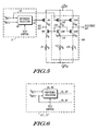
- FIG. 3 Illustrated in FIG. 3 is another memory, memory 60, having a different scheme for the sense amplifier wherein a common current is used rather than a common gate to accomplish biasing for the sense amplifier.
- a P-channel transistor 64 has a source connected to a V DD voltage terminal, and a gate connected at a node 62 to an output of a Reference Selection circuit 80 of Reference Circuit 77.
- a drain of transistor 64 provides a BIT OUT signal and is connected to a drain of an N-channel transistor 68.
- a source of transistor 68 is coupled to a first terminal of a memory cell 72 having a bit resistance of R B .
- the source of transistor 68 may be directly connected to memory cell 72 or may be coupled via column select and/or row select circuitry.
- a second terminal of memory cell 72 may be connected to a supply voltage terminal for receiving V SS or may be coupled via column select and/or row select circuitry.
- a P-channel transistor 66 has a source connected to a terminal for receiving V DD .
- a gate of transistor 66 is connected to a node 63 in Reference Circuit 77 and to a first reference voltage V REF1 , and a drain of transistor 66 provides the REFERENCE OUT signal and is connected to both a gate and a drain of diode-connected N-channel transistor 70.
- the gate of transistor 70 is connected to a gate of transistor 68 at a node 78.
- a source of transistor 70 is coupled to a first terminal of a reference memory cell 74 having a reference resistance value of R R .
- a memory reference circuit 76 is formed by transistor 66, transistor 70 and reference memory cell 74.
- a second terminal of reference memory cell 74 is coupled to the terminal for receiving the V SS supply voltage.
- the first terminal and the second terminal of reference memory cell 74 may be directly connected respectively to transistor 70 and the V SS supply voltage terminal or may be coupled via column select and/or row select circuitry (not shown).
- a first input of the Reference Selection circuit 80 is connected to the V REF1 signal, and a second input of the Reference Selection circuit 80 is connected to a V REF2 signal.
- V REF1 biases transistor 66 with a known voltage to establish a reference current I R1 through transistor 66.
- the current I R1 further biases diode connected transistor 70 establishing a voltage on node 78.
- the current I R1 continues through transistor 70 to the reference memory cell 74.
- transistors 68 and 70 are physically sized the same with large gate width/length ratios so that the gate/source voltage can be approximated by the threshold voltage of the transistors 68 and 70.
- the voltage across reference memory cell 74 and bit cell 72 is approximately the same.
- the bit cell resistance R B generates a current I B .
- the TEST CONTROL signal causes V REF1 to be placed on node 62.
- Transistor 64 is designed to match transistor 66 so that in this case current I R2 is the same as current I R1 . If the bit resistance R B is in the low state such that resistance R B is less than resistance R R , then current I B will be greater than I R1 . The voltage at BIT OUT will be less than the voltage of the REFERENCE OUT signal. If on the other hand, the bit resistance R B is in the high state such that resistance R B is greater than resistance R R , then current I B will be lower than I R1 . The voltage at BIT OUT will be greater than the voltage of the REFERENCE OUT signal.
- the bit resistance varies. Some bits in the low state may have a resistance value that is slightly less than or equal to the reference value and passes standard testing. Similarly, other bits in the high state may have a resistance near or slightly greater than the reference resistance thus marginally passing standard testing.
- the TEST CONTROL signal enables a test mode such that the Reference Selection circuit 80 supplies V REF2 to node 62. An appropriate value of V REF2 causes weak bits to fail.
- Memory cell 72 may have a low state resistance value near the reference resistance value such that I B is only slightly more than I R2 . Applying a value of V REF2 less than V REF1 will increase I R2 , thus I B for a weak bit will be less than I R2 and the weak bit fails.
- memory cell 72 may have a high state resistance value near the reference resistance value such that I B is only slightly less than I R2 . Applying a value of V REF2 greater than V REF1 will decrease I R2 , thus I B for a weak bit will be greater than I R2 and the weak bit fails.
- a memory reference circuit 81 has a P-channel transistor 82 having a source connected to a terminal for receiving supply voltage V DD .
- a gate of transistor 82 is connected to a drain thereof and is connected to a gate of transistor 20 and to a gate of a P-channel transistor 84.
- a source of transistor 84 is connected to the terminal for receiving supply voltage V DD .
- the drain of transistor 82 is connected to a drain of an N-channel transistor 88.
- the first reference voltage, V REF1 and a node 31 of Reference Circuit 13 is connected to a gate of transistor 88 and to a gate of an N-channel transistor 92 that are connected together.
- a drain of transistor 84 is connected to a reference output terminal, REFERENCE OUT, and to a drain of transistor 92.
- Each of transistors 88 and 92 has its source connected together.
- the source of transistor 88 is coupled to a first terminal of a high reference memory cell 90 having a resistance R H .
- a second terminal of reference memory cell 90 is coupled to the V SS voltage terminal.
- a source of transistor 92 is coupled to a first terminal of a low reference memory cell 94 having a resistance R L .
- a second terminal of reference memory cell 94 is coupled to the V SS supply voltage terminal.
- Memory cells 90 and 94 are coupled between the V SS supply voltage terminal and transistors 88 and 92, respectively, by column select and row select circuitry (not shown) as indicated by the dotted lines. All remaining circuitry of the memory of FIG. 4 is connected as previously described for FIG. 1 and has the same element numbering.
- memory reference circuit 81 performs a same function as the memory reference cell 12 of FIG. 1.
- the TEST CONTROL signal is set so the Vref1 voltage input is applied to node 30.
- the gates of transistors 16, 88 and 92 have the same voltage applied thereto.
- the transistors 16, 88 and 92 are physically sized the same with large gate width/length ratios so that the gate/source voltage can be approximated by the threshold voltage of the transistors 16, 88 and 92.
- the bit resistance R B and reference resistances R H and R L have approximately the same voltage across their terminals.
- the bit resistance R B has a low resistance state and a high resistance state.
- the reference resistance R L is manufactured to be similar to the low resistance state of R B and the reference resistance R H is manufactured to be similar to the high resistance state of R B .
- the voltage across the parallel combination of R L and R H generates a current, 2I R .
- Current I R passes through each of transistors 88 and 92.
- the current I R conducted by transistor 82 determines the voltage on the gate and drain of transistor 82 as a result of transistor 82 being diode connected.
- Transistors 20 and 84 are connected to mirror the current I R conducted by transistor 82.
- bit resistance R B is in the low resistance state. Then the bit current I B through memory cell 14 and transistor 16 will be larger than the reference current I R . The net result is that the voltage on BIT OUT will be lower than the voltage on REFERENCE OUT indicating a low resistance state.
- bit resistance R B is in the high resistance state. Then the bit current I B through memory cell 14 and transistor 16 will be smaller than the reference current I R through reference cell 28. The net result is that the voltage on BIT OUT will be higher than the voltage on REFERENCE OUT indicating a high resistance state.
- the bit resistance varies. Some bits in the low state may have a resistance value that is slightly less than or equal to the reference value and pass standard testing. Similarly, other bits in the high state may have a resistance near or slightly greater than the reference resistance thus marginally passing standard testing.
- the TEST CONTROL signal enables a test mode such that the Reference Selection circuit 18 supplies V REF2 to node 30. An appropriate value of V REF2 causes weak bits to fail.
- Memory cell 14 may have a low state resistance value near the reference resistance value such that I B is only slightly more than I R . Applying a value of V REF2 less than V REF1 will decrease I B , thus I B for a weak bit is less than I R and the weak bit fails.
- memory cell 14 may have a high state resistance value near the reference resistance value such that I B is only slightly greater than I R . Applying a value of V REF2 greater than V REF1 will increase I B , thus I B for a weak bit is greater than I R and the weak bit fails.
- a memory reference circuit 100 has a P-channel transistor 102 having a source connected to a power supply voltage terminal for receiving supply voltage V DD .
- a gate of transistor 102 is connected to a node 63 of a reference circuit 77 and to a first reference voltage, VREF1, and to a first input of the Reference Selection circuit 80.
- a drain of transistor 102 is connected to a drain of an N-channel transistor 106 at a node 105.
- a gate of transistor 106 is connected to the gate of transistor 68 and to the drain of transistor 106 at node 105.
- a source of transistor 106 is coupled to a first terminal of a reference memory cell 112 having a high resistive value R H .
- the connection may be either direct or coupled via one or both of column select circuitry and row select circuitry (not shown).
- a second terminal of reference memory cell 112 is coupled via one or both of column select circuitry and row select circuit (not shown) or is directly connected to a reference voltage terminal for receiving a voltage V SS .
- a source of a P-channel transistor 104 is connected to the power supply voltage terminal for receiving V DD .
- a gate of transistor 104 is connected in common to the gate of transistor 102 and to the first reference voltage, V REF1 .
- a drain of transistor 104 provides a REFERENCE OUT signal and is connected to a drain of an N-channel transistor 108.
- a gate of transistor 108 is connected to node 105, and a source of transistor 108 is connected to the source of transistor 106 at a node 110.
- the source of transistor 108 is also coupled to a first terminal of a reference memory cell 114 having a low resistive value R L .
- the connection may be either direct or coupled via one or both column select circuitry and row select circuitry (not shown).
- a second terminal of reference memory cell 114 is coupled via one or both of column select circuitry and row select circuitry (not shown) or is directly connected to the reference voltage terminal for receiving voltage V SS .
- V REF1 biases transistors 102 and 104 with a known voltage to respectively establish equal reference currents I R1 through transistors 102 and 104.
- the current I R1 further biases diode connected transistor 106 establishing a voltage on node 105.
- the current I R1 respectively continues through transistors 106 and 108 to the reference memory cells 112 and 114.
- transistors 68, 106 and 108 are physically sized the same with large gate width/length ratios so that the gate/source voltage can be approximated by the threshold voltage of the transistors 68, 106 and 108.
- the voltages across reference memory cells 112 and 114 and bit cell 72 are approximately the same.
- the bit cell resistance R B generates a current I B .
- the TEST CONTROL signal causes V REF1 to be placed on node 62.
- Transistor 64 is designed to match transistors 102 and 104 so that in this case current I R2 is the same as current I R1 . If the bit resistance R B is in the low state such that resistance R B is less than the average of resistances R H and R L , then current I B will be greater than IR 1 . The voltage at BIT OUT will be less than the voltage of the REFERENCE OUT signal. If on the other hand, the bit resistance R B is in the high state such that resistance R B is greater than the average of resistances R H and R L , then current I B will be lower than I R1 . The voltage at BIT OUT will be greater than the voltage of the REFERENCE OUT signal.
- the bit resistance varies. Some bits in the low state may have a resistance value that is slightly less than or equal to the reference value and pass standard testing. Similarly, other bits in the high state may have a resistance near or slightly greater than the reference resistance thus marginally passing standard testing.
- the TEST CONTROL signal enables a test mode such that the reference selection circuit 80 supplies V REF2 to node 62. An appropriate value of V REF2 causes weak bits to fail.
- Memory cell 72 may have a low state resistance value near the reference resistance value such that I B is only slightly more than I R . Applying a value of V REF2 less than V REF1 will increase I R2 , and thus I B for the weak bit will be less than I R2 and the weak bit will fail.
- memory cell 72 may have a high state resistance value near the reference resistance value such that I B is only slightly less than I R . Applying a value of V REF2 greater than V REF1 will decrease I R2 , and thus I B for the weak bit will be greater than I R2 and the weak bit will fail.
- FIG. 6 Illustrated in FIG. 6 is an alternative form of the Reference Circuits 13 and 77 of FIGs. 1, 3, 4 and 5 designated as Reference Circuit 13' or 77'.
- the first reference voltage, V REF1 is connected to a first input of Reference Selection circuit 18, 80.
- the second reference voltage, V REF2 is connected to a second input of Reference Selection circuit 18, 80 and to node 30, 62.
- the output of Reference Selection Circuit 18, 80 is connected to node 31, 63.
- a test control signal, TEST CONTROL is connected to a control terminal of Reference Selection Circuit 18, 80 for controlling whether input V REF1 or input V REF2 is placed on node 31, 63 by Reference Selection Circuit 18, 80.
- this alternative form places the V REF2 reference voltage on node 31, 63 and node 30, 62 in normal mode rather than placing V REF1 on both node 31, 63 and node 30, 62 as is the case in FIGS. 1, 3, 4 and 5.
- VREF1 is placed on node 31, 63 and VREF2 is placed on node 30, 62 as is the case described above in FIGS. 1, 3, 4 and 5. Therefore, operationally the function is the same in the test mode for each embodiment as explained above.
- a memory having cells with at least two distinct resistive states such as an MRAM, and circuitry used to identify weak bits that may provide inaccurate values when read.
- the indication may be accomplished without use of external factors, such as temperature and supply voltage variations, and without having to modify the timing and clock signals of the memory.
- the method provided herein causes the sense amplifier to be unbalanced under control of logic circuitry and a second reference voltage or current.
- the memory test circuitry provided herein enables improved reliability in operation and minimizes the presence of spurious weak bit errors exemplified by previously known methods.
- the detection of borderline resistance bits made possible by the present invention results in a reliable memory that will not generate errors due to the presence of weak memory cell bits.
- the memory may be repaired by using memory redundancy. Depending upon the number of weak bits identified, the memory may be repaired via redundancy, or if there is insufficient redundancy remaining, the memory may be failed.
- Reference voltage selection circuitry provided by Reference Selection circuits 18 and 80 herein may be implemented either as a multiplexor circuit or by using various logic circuits to implement the function of providing one of two reference voltages of predetermined value in response to a control signal.
- plurality is defined as two or more than two.
- another is defined as at least a second or more.
- including and/or having, as used herein, are defined as comprising (i.e., open language).
- coupled is defined as connected, although not necessarily directly, and not necessarily mechanically.
Landscapes
- Engineering & Computer Science (AREA)
- Computer Hardware Design (AREA)
- For Increasing The Reliability Of Semiconductor Memories (AREA)
- Read Only Memory (AREA)
Claims (11)
- Mémoire (10) qui présente au moins deux états de résistance, comprenant :une cellule de mémoire (14) ;une première cellule de mémoire de référence (28) ;un circuit de sélection de tension de référence (18) qui comporte une première entrée pour recevoir une première tension de référence, une seconde entrée pour recevoir une seconde tension de référence, une troisième entrée pour recevoir un signal de commande (TEST) et une sortie pour appliquer soit la première tension de référence, soit la seconde tension de référence sur la base du signal de commande ;un premier transistor (16) d'un premier type de conductivité qui comporte une première électrode de courant qui est couplée à la cellule de mémoire, une seconde électrode de courant et une électrode de commande qui est couplée à la sortie du circuit de sélection de tension de référence (18) pour recevoir soit la première tension de référence, soit la seconde tension de référence ;un second transistor (20) d'un second type de conductivité qui comporte une première électrode de courant qui est couplée à la seconde électrode de courant du premier transistor, une seconde électrode de courant qui est couplée à une première borne de tension et une électrode de commande ;un troisième transistor (26) du premier type de conductivité qui comporte une première électrode de courant qui est couplée à la première cellule de mémoire de référence, une électrode de commande qui est couplée pour recevoir la première tension de référence et une seconde électrode de courant ; etun quatrième transistor (22) du second type de conductivité qui comporte une première électrode de courant qui est couplée à la seconde électrode de courant du troisième transistor, une électrode de commande qui est couplée à la première électrode de courant du quatrième transistor et à l'électrode de commande du second transistor et une seconde électrode de courant qui est couplée à la première borne de tension, caractérisé en outre en ce que :le circuit de sélection de tension de référence (18) modifie de façon sélective la seconde tension de référence pour générer une valeur de seconde tension de référence modifiée pour un couplage sur l'électrode de commande du premier transistor (16).
- Mémoire selon la revendication 1, comprenant en outre:une seconde cellule de mémoire de référence (94) ;un cinquième transistor (92) du premier type de conductivité qui comporte une première électrode de courant qui est couplée à la seconde cellule de mémoire de référence ainsi qu'à la première électrode de courant du troisième transistor, une électrode de commande qui est couplée à l'électrode de commande du troisième transistor et une seconde électrode de courant ; etun sixième transistor (84) du second type de conductivité qui comporte une première électrode de courant qui est couplée à la seconde électrode de courant du cinquième transistor, une électrode de commande qui est couplée à l'électrode de commande du quatrième transistor et une seconde électrode de courant qui est couplée à la première borne de tension.
- Mémoire selon la revendication 2, dans laquelle la cellule de mémoire (14) est programmable selon soit un état de résistance élevée, soit un état de résistance faible, la première cellule de mémoire de référence (28, 90) est programmée dans l'état de résistance élevée et la seconde cellule de mémoire de référence (94) est programmée dans l'état de résistance faible.
- Mémoire selon la revendication 1, dans laquelle le circuit de sélection de tension de référence (18) applique la première tension de référence sur l'électrode de commande du premier transistor lorsque le signal de commande présente une première valeur et la seconde tension de référence sur l'électrode de commande du premier transistor lorsque le signal de commande présente une seconde valeur.
- Mémoire selon la revendication 1, dans laquelle la cellule de mémoire est programmable selon soit un état de résistance élevée, soit une état de résistance faible et la première cellule de mémoire de référence (28, 90) est programmée à une résistance prédéterminée.
- Mémoire selon la revendication 5, dans laquelle la résistance prédéterminée est une valeur qui est différente à la fois de l'état de résistance élevée et de l'état de résistance faible.
- Mémoire selon la revendication 1, dans laquelle la seconde tension de référence présente une valeur qui est différente de celle de la première tension de référence.
- Mémoire selon la revendication 1, dans laquelle la seconde électrode de courant du premier transistor (16) applique un signal de sortie et la seconde électrode de courant du troisième transistor (26) applique un signal de sortie de référence.
- Procédé de test d'une mémoire (10) qui présente au moins deux états de résistance, dans lequel la mémoire inclut une cellule de mémoire (14) qui est programmable selon n'importe lequel des au moins deux états de résistance, un premier transistor (16) qui comporte une première électrode de courant qui est couplée à la cellule de mémoire, une seconde électrode de courant qui est couplée à une borne de tension et une électrode de commande, une cellule de mémoire de référence (28) qui est programmée à une résistance prédéterminée et un second transistor (26) qui comporte une première électrode de courant qui est couplée à la cellule de mémoire de référence, une seconde électrode de courant qui est couplée à la borne de tension et une électrode de commande, le procédé comprenant :l'écriture d'un premier état pris parmi les au moins deux états de résistance sur la cellule de mémoire (14) ;l'application d'une valeur de première tension de référence sur l'électrode de commande du second transistor (26) et d'une valeur de seconde tension de référence qui est différente de la valeur de première tension de référence sur l'électrode de commande du premier transistor (16) ; etaprès l'application des valeurs de première et seconde tensions de référence, la détermination de si oui ou non la cellule de mémoire (14) est programmée selon le premier des au moins deux états de résistance, caractérisé en outre par les étapes de :modification de la valeur de seconde tension de référence de manière à générer une valeur de seconde tension de référence modifiée ;application de la valeur de seconde tension de référence modifiée qui est différente de la valeur de première tension de référence sur l'électrode de commande du premier transistor (16) ;après l'application de la valeur de seconde tension de référence modifiée, détermination de si oui ou non la cellule de mémoire (14) est programmée selon le premier des au moins deux états de résistance.
- Procédé selon la revendication 9, comprenant en outre:l'écriture d'un second état des au moins deux états de résistance sur la cellule de mémoire (14) ;l'application de la valeur de première tension de référence sur l'électrode de commande du second transistor (26) ;l'application d'une valeur de troisième tension de référence qui est différente des valeurs des première et seconde tensions de référence sur l'électrode de commande du premier transistor (16) ; etaprès l'application des valeurs des première et troisième tensions de référence, détermination de si oui ou non la cellule de mémoire (14) est programmée selon le second état des au moins deux états de résistance.
- Procédé selon la revendication 9, dans lequel les au moins deux états de résistance comprennent un état de résistance élevée et un état de résistance faible et dans lequel, lorsque le premier état des au moins deux états de résistance est l'état de résistance faible, la valeur de seconde tension de référence est inférieure à la valeur de première tension de référence et lorsque le premier état des au moins deux états de résistance est l'état de résistance élevée, la valeur de seconde tension de référence est supérieure à la valeur de première tension de référence.
Applications Claiming Priority (3)
| Application Number | Priority Date | Filing Date | Title |
|---|---|---|---|
| US10/255,303 US6538940B1 (en) | 2002-09-26 | 2002-09-26 | Method and circuitry for identifying weak bits in an MRAM |
| US255303 | 2002-09-26 | ||
| PCT/US2003/022851 WO2004029987A1 (fr) | 2002-09-26 | 2003-07-22 | Procede et circuit d'identification de bits faibles dans une memoire vive magnetique |
Publications (2)
| Publication Number | Publication Date |
|---|---|
| EP1547094A1 EP1547094A1 (fr) | 2005-06-29 |
| EP1547094B1 true EP1547094B1 (fr) | 2007-01-10 |
Family
ID=22967712
Family Applications (1)
| Application Number | Title | Priority Date | Filing Date |
|---|---|---|---|
| EP03798674A Expired - Lifetime EP1547094B1 (fr) | 2002-09-26 | 2003-07-22 | Procede et circuit d'identification de bits faibles dans une memoire vive magnetique |
Country Status (9)
| Country | Link |
|---|---|
| US (1) | US6538940B1 (fr) |
| EP (1) | EP1547094B1 (fr) |
| JP (1) | JP4322809B2 (fr) |
| KR (1) | KR100985400B1 (fr) |
| CN (1) | CN100416706C (fr) |
| AU (1) | AU2003252100A1 (fr) |
| DE (1) | DE60311117T2 (fr) |
| TW (1) | TWI299870B (fr) |
| WO (1) | WO2004029987A1 (fr) |
Families Citing this family (18)
| Publication number | Priority date | Publication date | Assignee | Title |
|---|---|---|---|---|
| US6600690B1 (en) * | 2002-06-28 | 2003-07-29 | Motorola, Inc. | Sense amplifier for a memory having at least two distinct resistance states |
| JP4266297B2 (ja) * | 2002-09-05 | 2009-05-20 | 株式会社ルネサステクノロジ | 不揮発性記憶装置 |
| US6707710B1 (en) * | 2002-12-12 | 2004-03-16 | Hewlett-Packard Development Company, L.P. | Magnetic memory device with larger reference cell |
| US6999887B2 (en) * | 2003-08-06 | 2006-02-14 | Infineon Technologies Ag | Memory cell signal window testing apparatus |
| KR100988087B1 (ko) * | 2003-11-24 | 2010-10-18 | 삼성전자주식회사 | Mram 특성 분석 장치 및 그 분석 방법 |
| US7038959B2 (en) * | 2004-09-17 | 2006-05-02 | Freescale Semiconductor, Inc. | MRAM sense amplifier having a precharge circuit and method for sensing |
| US7110313B2 (en) * | 2005-01-04 | 2006-09-19 | Taiwan Semiconductor Manufacturing Company, Ltd. | Multiple-time electrical fuse programming circuit |
| US7950069B2 (en) * | 2005-11-16 | 2011-05-31 | Eun Hyo Cho | Pants having body-shaping function |
| US7313043B2 (en) * | 2005-11-29 | 2007-12-25 | Altis Semiconductor Snc | Magnetic Memory Array |
| WO2009058148A1 (fr) * | 2007-11-01 | 2009-05-07 | Freescale Semiconductor Inc. | Contrôle de mémoire vive magnétique |
| US8780657B2 (en) | 2012-03-01 | 2014-07-15 | Apple Inc. | Memory with bit line current injection |
| US9165629B2 (en) * | 2013-03-12 | 2015-10-20 | Taiwan Semiconductor Manufacturing Co., Ltd. | Method and apparatus for MRAM sense reference trimming |
| KR102150469B1 (ko) * | 2014-04-04 | 2020-09-02 | 에스케이하이닉스 주식회사 | 저항성 메모리 장치 |
| US10290327B2 (en) * | 2017-10-13 | 2019-05-14 | Nantero, Inc. | Devices and methods for accessing resistive change elements in resistive change element arrays |
| US10224088B1 (en) * | 2018-02-12 | 2019-03-05 | Nxp Usa, Inc. | Memory with a global reference circuit |
| US10839879B2 (en) * | 2018-09-27 | 2020-11-17 | Taiwan Semiconductor Manufacturing Co., Ltd. | Read techniques for a magnetic tunnel junction (MTJ) memory device with a current mirror |
| CN112349321B (zh) * | 2019-08-06 | 2024-03-12 | 上海磁宇信息科技有限公司 | 一种使用公共参考电压的磁性随机存储器芯片架构 |
| US12027224B2 (en) | 2022-03-16 | 2024-07-02 | International Business Machines Corporation | Authenticity and yield by reading defective cells |
Family Cites Families (11)
| Publication number | Priority date | Publication date | Assignee | Title |
|---|---|---|---|---|
| US4468759A (en) | 1982-05-03 | 1984-08-28 | Intel Corporation | Testing method and apparatus for dram |
| US5142495A (en) * | 1989-03-10 | 1992-08-25 | Intel Corporation | Variable load for margin mode |
| US5321842A (en) * | 1990-01-13 | 1994-06-14 | At&T Bell Laboratories | Three-state driver with feedback-controlled switching |
| US6105152A (en) | 1993-04-13 | 2000-08-15 | Micron Technology, Inc. | Devices and methods for testing cell margin of memory devices |
| US5537358A (en) | 1994-12-06 | 1996-07-16 | National Semiconductor Corporation | Flash memory having adaptive sensing and method |
| US5731733A (en) * | 1995-09-29 | 1998-03-24 | Intel Corporation | Static, low current sensing circuit for sensing the state of a fuse device |
| FR2760888B1 (fr) * | 1997-03-11 | 1999-05-07 | Sgs Thomson Microelectronics | Circuit de lecture pour memoire adapte a la mesure des courants de fuite |
| US6128239A (en) * | 1999-10-29 | 2000-10-03 | Hewlett-Packard | MRAM device including analog sense amplifiers |
| US6317376B1 (en) * | 2000-06-20 | 2001-11-13 | Hewlett-Packard Company | Reference signal generation for magnetic random access memory devices |
| JP3596808B2 (ja) | 2000-08-10 | 2004-12-02 | 沖電気工業株式会社 | 不揮発性半導体記憶装置 |
| US6456524B1 (en) * | 2001-10-31 | 2002-09-24 | Hewlett-Packard Company | Hybrid resistive cross point memory cell arrays and methods of making the same |
-
2002
- 2002-09-26 US US10/255,303 patent/US6538940B1/en not_active Expired - Fee Related
-
2003
- 2003-07-22 DE DE60311117T patent/DE60311117T2/de not_active Expired - Fee Related
- 2003-07-22 KR KR1020057005218A patent/KR100985400B1/ko not_active IP Right Cessation
- 2003-07-22 EP EP03798674A patent/EP1547094B1/fr not_active Expired - Lifetime
- 2003-07-22 CN CNB038229684A patent/CN100416706C/zh not_active Expired - Fee Related
- 2003-07-22 WO PCT/US2003/022851 patent/WO2004029987A1/fr active IP Right Grant
- 2003-07-22 JP JP2004539810A patent/JP4322809B2/ja not_active Expired - Fee Related
- 2003-07-22 AU AU2003252100A patent/AU2003252100A1/en not_active Abandoned
- 2003-09-10 TW TW092125077A patent/TWI299870B/zh not_active IP Right Cessation
Also Published As
| Publication number | Publication date |
|---|---|
| JP4322809B2 (ja) | 2009-09-02 |
| KR20050057585A (ko) | 2005-06-16 |
| TWI299870B (en) | 2008-08-11 |
| US6538940B1 (en) | 2003-03-25 |
| WO2004029987A1 (fr) | 2004-04-08 |
| DE60311117D1 (de) | 2007-02-22 |
| JP2006500725A (ja) | 2006-01-05 |
| AU2003252100A1 (en) | 2004-04-19 |
| DE60311117T2 (de) | 2007-08-16 |
| KR100985400B1 (ko) | 2010-10-06 |
| TW200423140A (en) | 2004-11-01 |
| CN1685445A (zh) | 2005-10-19 |
| CN100416706C (zh) | 2008-09-03 |
| EP1547094A1 (fr) | 2005-06-29 |
Similar Documents
| Publication | Publication Date | Title |
|---|---|---|
| EP1547094B1 (fr) | Procede et circuit d'identification de bits faibles dans une memoire vive magnetique | |
| KR100591026B1 (ko) | 퓨즈 검출 회로를 갖는 집적 회로 메모리 | |
| US9747965B2 (en) | Adaptive reference scheme for magnetic memory applications | |
| EP0933785B1 (fr) | Dispositif semi-conducteur et méthode de detection de courant d'alimentation | |
| US7307911B1 (en) | Apparatus and method for improving sensing margin of electrically programmable fuses | |
| US6230292B1 (en) | Devices and method for testing cell margin of memory devices | |
| US6501692B1 (en) | Circuit and method for stress testing a static random access memory (SRAM) device | |
| US5124945A (en) | Method and apparatus for verifying the state of a plurality of electrically programmable memory cells | |
| US20070171762A1 (en) | Method and Apparatus to Control Sensing Time for Nonvolatile Memory | |
| US6983404B2 (en) | Method and apparatus for checking the resistance of programmable elements | |
| US7586788B2 (en) | Nonvolatile semiconductor memory having voltage adjusting circuit | |
| KR100426909B1 (ko) | 반도체 장치 | |
| US4586170A (en) | Semiconductor memory redundant element identification circuit | |
| US6501691B2 (en) | Word-line deficiency detection method for semiconductor memory device | |
| US6670843B1 (en) | Method and apparatus for sensing a programming state of fuses | |
| US7447057B2 (en) | Semiconductor integrated circuit device with a plurality of memory cells storing data | |
| US8614921B2 (en) | Nonvolatile semiconductor memory device | |
| US6483744B2 (en) | Multi-state non-volatile semiconductor memory device | |
| US20030223282A1 (en) | Redundancy circuit and method for semiconductor memory devices | |
| US7020035B1 (en) | Measuring and correcting sense amplifier and memory mismatches using NBTI | |
| US7177217B2 (en) | Method and circuit for verifying and eventually substituting defective reference cells of a memory | |
| JP2007026477A (ja) | 不揮発性記憶装置 | |
| JP3904642B2 (ja) | 集積回路アレイ内の欠陥を検出する方法 | |
| US6535441B2 (en) | Static semiconductor memory device capable of accurately detecting failure in standby mode | |
| US7929363B1 (en) | Memory test and setup method |
Legal Events
| Date | Code | Title | Description |
|---|---|---|---|
| PUAI | Public reference made under article 153(3) epc to a published international application that has entered the european phase |
Free format text: ORIGINAL CODE: 0009012 |
|
| 17P | Request for examination filed |
Effective date: 20050426 |
|
| AK | Designated contracting states |
Kind code of ref document: A1 Designated state(s): AT BE BG CH CY CZ DE DK EE ES FI FR GB GR HU IE IT LI LU MC NL PT RO SE SI SK TR |
|
| AX | Request for extension of the european patent |
Extension state: AL LT LV MK |
|
| DAX | Request for extension of the european patent (deleted) | ||
| GRAP | Despatch of communication of intention to grant a patent |
Free format text: ORIGINAL CODE: EPIDOSNIGR1 |
|
| GRAS | Grant fee paid |
Free format text: ORIGINAL CODE: EPIDOSNIGR3 |
|
| GRAA | (expected) grant |
Free format text: ORIGINAL CODE: 0009210 |
|
| AK | Designated contracting states |
Kind code of ref document: B1 Designated state(s): AT BE BG CH CY CZ DE DK EE ES FI FR GB GR HU IE IT LI LU MC NL PT RO SE SI SK TR |
|
| PG25 | Lapsed in a contracting state [announced via postgrant information from national office to epo] |
Ref country code: AT Free format text: LAPSE BECAUSE OF FAILURE TO SUBMIT A TRANSLATION OF THE DESCRIPTION OR TO PAY THE FEE WITHIN THE PRESCRIBED TIME-LIMIT Effective date: 20070110 Ref country code: SI Free format text: LAPSE BECAUSE OF FAILURE TO SUBMIT A TRANSLATION OF THE DESCRIPTION OR TO PAY THE FEE WITHIN THE PRESCRIBED TIME-LIMIT Effective date: 20070110 Ref country code: FI Free format text: LAPSE BECAUSE OF FAILURE TO SUBMIT A TRANSLATION OF THE DESCRIPTION OR TO PAY THE FEE WITHIN THE PRESCRIBED TIME-LIMIT Effective date: 20070110 Ref country code: CH Free format text: LAPSE BECAUSE OF FAILURE TO SUBMIT A TRANSLATION OF THE DESCRIPTION OR TO PAY THE FEE WITHIN THE PRESCRIBED TIME-LIMIT Effective date: 20070110 Ref country code: DK Free format text: LAPSE BECAUSE OF FAILURE TO SUBMIT A TRANSLATION OF THE DESCRIPTION OR TO PAY THE FEE WITHIN THE PRESCRIBED TIME-LIMIT Effective date: 20070110 Ref country code: NL Free format text: LAPSE BECAUSE OF FAILURE TO SUBMIT A TRANSLATION OF THE DESCRIPTION OR TO PAY THE FEE WITHIN THE PRESCRIBED TIME-LIMIT Effective date: 20070110 Ref country code: LI Free format text: LAPSE BECAUSE OF FAILURE TO SUBMIT A TRANSLATION OF THE DESCRIPTION OR TO PAY THE FEE WITHIN THE PRESCRIBED TIME-LIMIT Effective date: 20070110 |
|
| REG | Reference to a national code |
Ref country code: GB Ref legal event code: FG4D |
|
| REG | Reference to a national code |
Ref country code: IE Ref legal event code: FG4D |
|
| REF | Corresponds to: |
Ref document number: 60311117 Country of ref document: DE Date of ref document: 20070222 Kind code of ref document: P |
|
| PG25 | Lapsed in a contracting state [announced via postgrant information from national office to epo] |
Ref country code: SE Free format text: LAPSE BECAUSE OF FAILURE TO SUBMIT A TRANSLATION OF THE DESCRIPTION OR TO PAY THE FEE WITHIN THE PRESCRIBED TIME-LIMIT Effective date: 20070410 |
|
| PG25 | Lapsed in a contracting state [announced via postgrant information from national office to epo] |
Ref country code: BG Free format text: LAPSE BECAUSE OF EXPIRATION OF PROTECTION Effective date: 20070411 |
|
| PG25 | Lapsed in a contracting state [announced via postgrant information from national office to epo] |
Ref country code: ES Free format text: LAPSE BECAUSE OF FAILURE TO SUBMIT A TRANSLATION OF THE DESCRIPTION OR TO PAY THE FEE WITHIN THE PRESCRIBED TIME-LIMIT Effective date: 20070421 |
|
| PG25 | Lapsed in a contracting state [announced via postgrant information from national office to epo] |
Ref country code: PT Free format text: LAPSE BECAUSE OF FAILURE TO SUBMIT A TRANSLATION OF THE DESCRIPTION OR TO PAY THE FEE WITHIN THE PRESCRIBED TIME-LIMIT Effective date: 20070611 |
|
| NLV1 | Nl: lapsed or annulled due to failure to fulfill the requirements of art. 29p and 29m of the patents act | ||
| ET | Fr: translation filed | ||
| REG | Reference to a national code |
Ref country code: CH Ref legal event code: PL |
|
| PLBE | No opposition filed within time limit |
Free format text: ORIGINAL CODE: 0009261 |
|
| STAA | Information on the status of an ep patent application or granted ep patent |
Free format text: STATUS: NO OPPOSITION FILED WITHIN TIME LIMIT |
|
| PG25 | Lapsed in a contracting state [announced via postgrant information from national office to epo] |
Ref country code: SK Free format text: LAPSE BECAUSE OF FAILURE TO SUBMIT A TRANSLATION OF THE DESCRIPTION OR TO PAY THE FEE WITHIN THE PRESCRIBED TIME-LIMIT Effective date: 20070110 |
|
| 26N | No opposition filed |
Effective date: 20071011 |
|
| PG25 | Lapsed in a contracting state [announced via postgrant information from national office to epo] |
Ref country code: CZ Free format text: LAPSE BECAUSE OF FAILURE TO SUBMIT A TRANSLATION OF THE DESCRIPTION OR TO PAY THE FEE WITHIN THE PRESCRIBED TIME-LIMIT Effective date: 20070110 Ref country code: RO Free format text: LAPSE BECAUSE OF FAILURE TO SUBMIT A TRANSLATION OF THE DESCRIPTION OR TO PAY THE FEE WITHIN THE PRESCRIBED TIME-LIMIT Effective date: 20070110 Ref country code: BE Free format text: LAPSE BECAUSE OF FAILURE TO SUBMIT A TRANSLATION OF THE DESCRIPTION OR TO PAY THE FEE WITHIN THE PRESCRIBED TIME-LIMIT Effective date: 20070110 |
|
| GBPC | Gb: european patent ceased through non-payment of renewal fee |
Effective date: 20070722 |
|
| PG25 | Lapsed in a contracting state [announced via postgrant information from national office to epo] |
Ref country code: MC Free format text: LAPSE BECAUSE OF NON-PAYMENT OF DUE FEES Effective date: 20070731 Ref country code: IT Free format text: LAPSE BECAUSE OF NON-PAYMENT OF DUE FEES Effective date: 20070722 Ref country code: DE Free format text: LAPSE BECAUSE OF NON-PAYMENT OF DUE FEES Effective date: 20080201 Ref country code: GR Free format text: LAPSE BECAUSE OF FAILURE TO SUBMIT A TRANSLATION OF THE DESCRIPTION OR TO PAY THE FEE WITHIN THE PRESCRIBED TIME-LIMIT Effective date: 20070411 |
|
| PG25 | Lapsed in a contracting state [announced via postgrant information from national office to epo] |
Ref country code: GB Free format text: LAPSE BECAUSE OF NON-PAYMENT OF DUE FEES Effective date: 20070722 |
|
| REG | Reference to a national code |
Ref country code: FR Ref legal event code: ST Effective date: 20080331 |
|
| PG25 | Lapsed in a contracting state [announced via postgrant information from national office to epo] |
Ref country code: FR Free format text: LAPSE BECAUSE OF NON-PAYMENT OF DUE FEES Effective date: 20070731 |
|
| PG25 | Lapsed in a contracting state [announced via postgrant information from national office to epo] |
Ref country code: IE Free format text: LAPSE BECAUSE OF NON-PAYMENT OF DUE FEES Effective date: 20070723 |
|
| PG25 | Lapsed in a contracting state [announced via postgrant information from national office to epo] |
Ref country code: EE Free format text: LAPSE BECAUSE OF FAILURE TO SUBMIT A TRANSLATION OF THE DESCRIPTION OR TO PAY THE FEE WITHIN THE PRESCRIBED TIME-LIMIT Effective date: 20070110 |
|
| PG25 | Lapsed in a contracting state [announced via postgrant information from national office to epo] |
Ref country code: CY Free format text: LAPSE BECAUSE OF FAILURE TO SUBMIT A TRANSLATION OF THE DESCRIPTION OR TO PAY THE FEE WITHIN THE PRESCRIBED TIME-LIMIT Effective date: 20070110 |
|
| PG25 | Lapsed in a contracting state [announced via postgrant information from national office to epo] |
Ref country code: LU Free format text: LAPSE BECAUSE OF NON-PAYMENT OF DUE FEES Effective date: 20070722 |
|
| PG25 | Lapsed in a contracting state [announced via postgrant information from national office to epo] |
Ref country code: TR Free format text: LAPSE BECAUSE OF FAILURE TO SUBMIT A TRANSLATION OF THE DESCRIPTION OR TO PAY THE FEE WITHIN THE PRESCRIBED TIME-LIMIT Effective date: 20070110 Ref country code: HU Free format text: LAPSE BECAUSE OF FAILURE TO SUBMIT A TRANSLATION OF THE DESCRIPTION OR TO PAY THE FEE WITHIN THE PRESCRIBED TIME-LIMIT Effective date: 20070711 |