EP1544899A2 - Nichtflüchtige Kapazität einer Halbleiterspeicheranordnung und deren Betriebsverfahren - Google Patents
Nichtflüchtige Kapazität einer Halbleiterspeicheranordnung und deren Betriebsverfahren Download PDFInfo
- Publication number
- EP1544899A2 EP1544899A2 EP04257827A EP04257827A EP1544899A2 EP 1544899 A2 EP1544899 A2 EP 1544899A2 EP 04257827 A EP04257827 A EP 04257827A EP 04257827 A EP04257827 A EP 04257827A EP 1544899 A2 EP1544899 A2 EP 1544899A2
- Authority
- EP
- European Patent Office
- Prior art keywords
- layer
- phase
- capacitor
- transition
- memory device
- Prior art date
- Legal status (The legal status is an assumption and is not a legal conclusion. Google has not performed a legal analysis and makes no representation as to the accuracy of the status listed.)
- Ceased
Links
Images


Classifications
-
- H—ELECTRICITY
- H10—SEMICONDUCTOR DEVICES; ELECTRIC SOLID-STATE DEVICES NOT OTHERWISE PROVIDED FOR
- H10D—INORGANIC ELECTRIC SEMICONDUCTOR DEVICES
- H10D84/00—Integrated devices formed in or on semiconductor substrates that comprise only semiconducting layers, e.g. on Si wafers or on GaAs-on-Si wafers
-
- B—PERFORMING OPERATIONS; TRANSPORTING
- B82—NANOTECHNOLOGY
- B82Y—SPECIFIC USES OR APPLICATIONS OF NANOSTRUCTURES; MEASUREMENT OR ANALYSIS OF NANOSTRUCTURES; MANUFACTURE OR TREATMENT OF NANOSTRUCTURES
- B82Y10/00—Nanotechnology for information processing, storage or transmission, e.g. quantum computing or single electron logic
-
- G—PHYSICS
- G11—INFORMATION STORAGE
- G11C—STATIC STORES
- G11C13/00—Digital stores characterised by the use of storage elements not covered by groups G11C11/00, G11C23/00, or G11C25/00
- G11C13/0002—Digital stores characterised by the use of storage elements not covered by groups G11C11/00, G11C23/00, or G11C25/00 using resistive RAM [RRAM] elements
- G11C13/0004—Digital stores characterised by the use of storage elements not covered by groups G11C11/00, G11C23/00, or G11C25/00 using resistive RAM [RRAM] elements comprising amorphous/crystalline phase transition cells
-
- H—ELECTRICITY
- H10—SEMICONDUCTOR DEVICES; ELECTRIC SOLID-STATE DEVICES NOT OTHERWISE PROVIDED FOR
- H10B—ELECTRONIC MEMORY DEVICES
- H10B12/00—Dynamic random access memory [DRAM] devices
- H10B12/01—Manufacture or treatment
- H10B12/02—Manufacture or treatment for one transistor one-capacitor [1T-1C] memory cells
- H10B12/03—Making the capacitor or connections thereto
- H10B12/033—Making the capacitor or connections thereto the capacitor extending over the transistor
-
- H—ELECTRICITY
- H10—SEMICONDUCTOR DEVICES; ELECTRIC SOLID-STATE DEVICES NOT OTHERWISE PROVIDED FOR
- H10B—ELECTRONIC MEMORY DEVICES
- H10B20/00—Read-only memory [ROM] devices
-
- H—ELECTRICITY
- H10—SEMICONDUCTOR DEVICES; ELECTRIC SOLID-STATE DEVICES NOT OTHERWISE PROVIDED FOR
- H10B—ELECTRONIC MEMORY DEVICES
- H10B63/00—Resistance change memory devices, e.g. resistive RAM [ReRAM] devices
- H10B63/30—Resistance change memory devices, e.g. resistive RAM [ReRAM] devices comprising selection components having three or more electrodes, e.g. transistors
-
- H—ELECTRICITY
- H10—SEMICONDUCTOR DEVICES; ELECTRIC SOLID-STATE DEVICES NOT OTHERWISE PROVIDED FOR
- H10B—ELECTRONIC MEMORY DEVICES
- H10B69/00—Erasable-and-programmable ROM [EPROM] devices not provided for in groups H10B41/00 - H10B63/00, e.g. ultraviolet erasable-and-programmable ROM [UVEPROM] devices
-
- H—ELECTRICITY
- H10—SEMICONDUCTOR DEVICES; ELECTRIC SOLID-STATE DEVICES NOT OTHERWISE PROVIDED FOR
- H10D—INORGANIC ELECTRIC SEMICONDUCTOR DEVICES
- H10D1/00—Resistors, capacitors or inductors
- H10D1/60—Capacitors
- H10D1/68—Capacitors having no potential barriers
-
- H—ELECTRICITY
- H10—SEMICONDUCTOR DEVICES; ELECTRIC SOLID-STATE DEVICES NOT OTHERWISE PROVIDED FOR
- H10N—ELECTRIC SOLID-STATE DEVICES NOT OTHERWISE PROVIDED FOR
- H10N70/00—Solid-state devices having no potential barriers, and specially adapted for rectifying, amplifying, oscillating or switching
- H10N70/20—Multistable switching devices, e.g. memristors
-
- H—ELECTRICITY
- H10—SEMICONDUCTOR DEVICES; ELECTRIC SOLID-STATE DEVICES NOT OTHERWISE PROVIDED FOR
- H10N—ELECTRIC SOLID-STATE DEVICES NOT OTHERWISE PROVIDED FOR
- H10N70/00—Solid-state devices having no potential barriers, and specially adapted for rectifying, amplifying, oscillating or switching
- H10N70/801—Constructional details of multistable switching devices
- H10N70/821—Device geometry
- H10N70/826—Device geometry adapted for essentially vertical current flow, e.g. sandwich or pillar type devices
-
- H—ELECTRICITY
- H10—SEMICONDUCTOR DEVICES; ELECTRIC SOLID-STATE DEVICES NOT OTHERWISE PROVIDED FOR
- H10N—ELECTRIC SOLID-STATE DEVICES NOT OTHERWISE PROVIDED FOR
- H10N70/00—Solid-state devices having no potential barriers, and specially adapted for rectifying, amplifying, oscillating or switching
- H10N70/801—Constructional details of multistable switching devices
- H10N70/881—Switching materials
- H10N70/883—Oxides or nitrides
- H10N70/8833—Binary metal oxides, e.g. TaOx
Definitions
- the present invention relates to a semiconductor device and a semiconductor memory device comprising the same, and more particularly, to a nonvolatile capacitor of a semiconductor device, a semiconductor memory device comprising the capacitor, and a method of operating the memory device.
- a semiconductor memory device basically comprises a transistor and a capacitor.
- various storage media have been developed as substitutes for capacitors.
- MTJ magnetic tunneling junction
- the semiconductor memory device has high integration, high operation speed, and nonvolatility superior enough not to lose data stored therein even after power is switched off.
- a dynamic random access memory (DRAM) has advantages of high integration and high operation speed, but does not has nonvolatility. Accordingly, the DRAM loses all data after power is switched off.
- a flash memory has nonvolatility in contrast to the DRAM, but has lower integration and operation speed than the DRAM.
- a capacitor of a semiconductor device comprising: a lower electrode; a dielectric layer stacked on the lower electrode and including a phase-transition layer, which displays two remarkably different resistance characteristics after insulating property on thereof is changed; and an upper electrode stacked on the dielectric layer.
- the dielectric layer may comprise a first insulating layer stacked on the lower electrode, the phase-transition layer stacked on the first insulating layer, and a second insulating layer stacked on the phase-transition layer.
- Each of the first and second insulating layers may be a dielectric layer with a dielectric constant greater than that of the phase-transition layer.
- the dielectric layer may be one of a silicon oxide layer, a tantalum oxide layer and an aluminum oxide layer.
- the phase-transition layer may be a dielectric layer, which displays two remarkably different resistance characteristics according to a range of an applied voltage while at least one component of the phase-transition layer is separated by electrons injected into the phase-transition layer.
- the phase-transition layer may be a niobium oxide layer.
- a thickness ratio of the first insulating layer, the phase-transition layer, and the second insulating layer may be 5:6:5.
- a semiconductor memory device including a transistor and a capacitor, the capacitor comprising: a lower electrode; a dielectric layer stacked on the lower electrode and including a phase-transition layer, which displays two remarkably different resistance characteristics after insulating property thereof is changed; and an upper electrode stacked on the dielectric layer.
- the dielectric layer may be the dielectric layer provided according to the one aspect of the present invention.
- a method of operating a semiconductor memory device including a transistor and a capacitor, wherein the capacitor comprises a lower electrode, a dielectric layer including a phase-transition layer, which displays two remarkably different resistance characteristics after insulating property thereof is changed, and an upper electrode, the method comprising: changing insulating property of the phase-transition layer; and applying a write voltage to the capacitor while leaving the transistor turned on.
- the insulating property of the phase-transition layer may be changed by injecting electrons to the phase-transition layer, and the electrons may be injected to the phase-transition layer by applying a voltage to the capacitor.
- a method of operating a semiconductor memory device including a transistor and a capacitor, wherein the capacitor comprises a lower electrode, a dielectric layer including a phase-transition layer, which displays two remarkably different resistance characteristics after insulating property thereof is changed, and an upper electrode, the method comprising: measuring a current by applying a read voltage to the capacitor while leaving the transistor turned on; and comparing the measured current value with a reference value.
- the semiconductor memory device has advantages of both a DRAM and a flash memory device, that is, is fast in data processing as the DRAM and is as nonvolatile as the flash memory device such that data stored therein are not lost even after power is switched off.
- the invention thus provides a nonvolatile capacitor of a semiconductor device, a nonvolatile semiconductor memory device comprising the capacitor, which is as fast in operation as a dynamic random access memory (DRAM) and has the same nonvolatile as a flash memory device.
- DRAM dynamic random access memory
- the present invention further provides a method of operating the semiconductor memory device
- a nonvolatile capacitor C of a semiconductor device includes a lower electrode 40, a dielectric layer 42, and an upper electrode 44.
- the lower electrode 40 may be a platinum electrode.
- the upper electrode 44 may be a ruthenium electrode.
- the lower electrode 40 and the upper electrode 44 may be made of different materials from each other, and the materials of the lower and upper electrodes 40 and 44 are generally determined by the kind of the dielectric layer 42.
- the dielectric layer 42 includes a first insulating layer 42a, a phase-transition layer 42b stacked on the first insulating layer 42a, and a second insulating layer 42c stacked on the phase-transition layer 42b.
- the first insulating layer 42a is a dielectric layer having a predetermined thickness and dielectric constant.
- the first insulating layer 42a may be a silicon oxide layer, a tantalum oxide layer, or an aluminium oxide layer.
- the second insulating layer 42c is preferably identical to the first insulating layer 42a but may be a dielectric layer different from the first insulating layer 42a.
- a voltage (referred to as a third voltage hereinafter) being applied to the phase-transition layer 42b of the capacitor C shown in FIG. 1 is equal to or greater than a voltage (referred to as a first voltage hereinafter) being applied to the first insulating layer 42a or a voltage (referred to as a second voltage hereinafter) being applied to the second insulating layer 42c.
- a voltage being applied to each component of the capacitor is inversely proportional to the capacitance of the component.
- the capacitances of the first insulating layer 42a and the second insulating layer 42c must be equal to or greater than the capacitance of the phase-transition layer 42b.
- the phase-transition layer 42b is a dielectric layer having a dielectric constant less than that of the first and second insulating layers 42a and 42c.
- the phase-transition layer 42b may be a niobium oxide layer (Nb2O5) of a predetermined thickness.
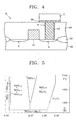
- phase-transition layer 42b is a niobium oxide layer showing various phases according to the content of oxygen as shown in FIG. 5
- electrons are injected to the phase-transition layer 42b such that at least one oxygen atom of the niobium oxide layer is separated and the insulating property of the phase-transition layer 42b is changed.
- the first and second insulating layers 42a and 42c prevent the separated oxygen atom from being discharged out of the phase-transition layer 42b.
- FIG. 2 is a graph illustrating resistance characteristics of a capacitor (referred to as a to-be-tested capacitor) comprising a platinum electrode as the lower electrode 40, a ruthenium electrode as the upper electrode 44, a tantalum oxide layer of 50 ⁇ as the first insulating layer 42a, a niobium oxide layer of 60 ⁇ as the phase-transition layer 42b, and a tantalum oxide layer of 50 ⁇ as the second insulating layer 42c.
- a capacitor referred to as a to-be-tested capacitor
- Symbols ⁇ and ⁇ in the graph of FIG. 2 represent a current change of the to-be-tested capacitor when a voltage is applied to the to-be-tested capacitor with the phase-transition layer 42 whose insulation is destroyed. That is, symbols ⁇ and ⁇ represent a resistance change of the to-be-tested capacitor.
- a current of the to-be-tested capacitor measured when the voltage is applied to the to-be-tested capacitor with the phase-transition layer 42b whose insulation is destroyed is approximately 10 -2 A.
- the voltage applied to the to-be-tested capacitor exceeds a predetermined value, for example, 2V
- the current of the to-be-tested capacitor drastically decreases to approximately 10 -11 A. This means that the resistance of the to-be-tested capacitor drastically increases.
- any high voltage is applied to the capacitor after the current of the to-be-tested capacitor decreases to approximately 10 -11 A, the current of the to-be-tested capacitor does not increase much.
- the to-be-tested capacitor with the phase-transition layer 42b whose insulation is destroyed is referred to as a first state capacitor
- a voltage when a relatively greater current is measured in the first state capacitor is referred to as a first voltage
- a voltage when a current fairly lower than the current at the first voltage is measured is referred to as a second voltage.
- Symbols ⁇ and O in the graph of FIG. 2 represent a current change of the first state capacitor when the current of the first state capacitor is drastically lowered by applying the second voltage to the first state capacitor and then the first voltage is applied to the first state capacitor.
- Data can be stored in a nonvolatile state in the capacitor C having such current characteristics, namely, resistance characteristics. For example, if the current of the first state capacitor is high, namely, if the resistance of the first state capacitor is low, it may be considered that an arbitrary data, e.g., a bit data 1, is written. If the resistance of the first state capacitor high, it may be considered that another arbitrary data, e.g., a bit data 0, is written.
- the endurance of the to-be-tested capacitor was tested.
- the endurance test was repeatedly performed by making the to-be-tested capacitor become the first state capacitor, decreasing or increasing the resistance of the first state capacitor, and measuring the current of the first state capacitor.
- FIG. 3 is a graph illustrating results of the endurance test.
- Symbol ⁇ in FIG. 3 represents a current (referred to as a first current hereinafter) measured when the resistance of the first state capacitor is low
- symbol O in FIG. 3 represents a current (referred to as a second current hereinafter) measured when the resistance of the first state capacitor is high.
- the first current and the second current vary whenever they are measured in the endurance test, but the second current is more than 10 times greater than the first current.
- a semiconductor memory device M comprising the capacitor C of FIG. 1 will now be explained with reference to FIG. 4.
- field oxide layers 52 are formed on predetermined areas of a substrate 50.
- a transistor is formed on the substrate 50 between the field oxide layers 52. That is, a gate 54 is formed on the substrate 50 between the field oxide layers 52.
- a source region S and a drain region D are respectively formed on the substrate 50 between the gate 54 and the field oxide layers 52 through implantation of conductive impurities.
- An interlayer insulating layer 56 e.g., a boron-phosphorous-silicate glass (BPSG) layer, is formed on the substrate 50 to cover the field oxide layers 52 and the transistor.
- a contact hole h is formed in the interlayer insulating layer 56.
- the drain region D is exposed by the contact hole h.
- the contact hole h is filled with a conductive plug 58.
- a diffusion barrier 60 is formed on the interlayer insulating layer 56 to cover the conductive plug 58.
- the capacitor C is formed on the diffusion barrier 60.
- the capacitor C preferably includes the lower electrode 40, the dielectric layer 42, and the upper electrode 44 as described with reference to FIG. 1.
- the diffusion barrier 60 may not be required.
- the capacitor may not be a simple stacked capacitor, but may be a more complex three-dimensional capacitor, such as a cylinder-type stacked capacitor.
- a method of manufacturing the aforesaid semiconductor memory device M may include forming the transistor on the substrate 50 in a typical way, forming the interlayer insulating layer 56 on the substrate 50 to cover the transistor, forming the contact hole h in the interlayer insulating layer 56 to expose the drain region D of the transistor, filling the contact hole h with the conductive plug 58, and forming the capacitor C on the interlayer insulating layer 56 to contact the conductive plug 58.
- the diffusion barrier 60 may be formed between the conductive plug 58 and the capacitor C. As shown in FIG.
- the capacitor C may be formed by forming the lower electrode 40, stacking the dielectric layer 42, which includes the first insulating layer 42a, the phase-transition layer 42b, and the second insulating layer 42c, on the lower electrode 40, and stacking the upper electrode 44 on the dielectric layer 42.
- the first insulating layer 42a may be a dielectric layer having a first thickness, for example, a silicon oxide layer, a tantalum oxide layer, or an aluminium oxide layer.
- the second insulating layer 42c may be a dielectric layer having a second thickness, for example, a silicon oxide layer, a tantalum layer, or a aluminium layer.
- the phase-transition layer 42b may be a dielectric layer having a third thickness and display different resistance characteristics according to a range of an applied voltage after the insulation thereof is destroyed by electrons injected thereinto.
- the phase-transition layer 42b may be an oxide layer of group-V atoms.
- a niobium layer is preferably used as the oxide layer of V-group atoms but other oxide layer can be used.
- the first, second, and third thicknesses can be the same, but it is preferable that a ratio of the first, second, and third thicknesses is 5:6:5.
- the phase-transition layer 42 may have a thickness of 60 ⁇ .
- the electrons used to cause a phase transition of the phase-transition layer 42b may be injected to the phase-transition layer 42b by applying a predetermined voltage to the capacitor C.
- the predetermined voltage applied to the capacitor C is a voltage at which the insulation of the phase-transition layer 42b is changed or destroyed.
- a voltage across the phase-transition layer 42b is equal to or greater than a voltage across the first and second insulating layers 42 and 44. Accordingly, it is preferable that the phase-transition layer 42b has a dielectric constant less than that of the dielectric layers used as the first and second insulating layers 42 and 44.
- the electrons used to destroy the insulation of the phase-transition layer 42b can be injected to the phase-transition layer 42b by externally applying electrons with energy, which is high enough to pass through the upper electrode 44 and reach the phase-transition layer 42b, to the capacitor C, instead of applying the predetermined voltage to the capacitor C.
- the insulation of the phase-transition layer 42b can also be destroyed by applying light beams, preferably, ultraviolet rays, with energy, which is high enough to separate some components, at least one oxygen, of the phase-transition layer, to the capacitor C.
- the first and second insulating layers 42a and 42c prevent the separated oxygen from being discharged out of the phase-transition layer 42b.
- a voltage capable of destroying the insulation of the dielectric layer of the capacitor C is applied to the capacitor C to destroy the insulation of the dielectric layer.
- the capacitor C becomes the first state capacitor having the resistance characteristics as described with reference to FIG. 2.
- the resistance of the first state capacitor is lowered, and if the second voltage is applied to the first state capacitor, the resistance of the first state capacitor is raised.
- the bit data 1 can be written by applying the first voltage to the first state capacitor, or the bit data 0 can be written by applying the second voltage to the first state capacitor.
- the written bit data values may be opposite.
- the resistance of the phase-transition layer 42 varies according to the written bit data. Accordingly, the transistor is turned on, and the current of the capacitor is measured by applying a predetermined read voltage to the capacitor.
- the measured current value is greater than a reference value, it is determined that the bit data 1 is read from the semiconductor memory device M. If the measured current value is less than the reference value, it is determined that the bit data 0 is read from the semiconductor memory device M.
- the bit data according to the measured current values may be opposite. That is, the bit data 1 may be the bit data 0, and the bit data 0 may be the bit data 1.
- the dielectric layer of the capacitor according to the present invention includes the phase-transition layer with two phases such that the phase-transition layer displays different resistance characteristics according to the range of the applied voltage and maintains the characteristics irrespective of the existence of the applied voltage after the insulation thereof is changed and destroyed by the injected electrons.
- the capacitor can be easily manufactured using the typical semiconductor manufacturing process, and an additional process is not needed. Consequently, when the capacitor of the present invention is applied to a general nonvolatile semiconductor memory device, such as a DRAM, the semiconductor memory device can maintain its original operation speed and have nonvolatile characteristics. That is, the semiconductor memory device comprising the capacitor according to the present invention can have advantages of both the DRAM and flash memory.
- the transistor may be a thin film transistor, and some of the layers constituting the dielectric layer 42 may be ferroelectric layers.
- a semiconductor memory device other than the semiconductor memory device shown in FIG. 4 may include the capacitor shown in FIG. 1. Accordingly, the present invention is defined by the following claims, not by the previously mentioned embodiments.
Landscapes
- Engineering & Computer Science (AREA)
- Chemical & Material Sciences (AREA)
- Nanotechnology (AREA)
- Crystallography & Structural Chemistry (AREA)
- Physics & Mathematics (AREA)
- Mathematical Physics (AREA)
- Theoretical Computer Science (AREA)
- Manufacturing & Machinery (AREA)
- Semiconductor Memories (AREA)
- Formation Of Insulating Films (AREA)
Applications Claiming Priority (2)
| Application Number | Priority Date | Filing Date | Title |
|---|---|---|---|
| KR1020030092614A KR100552704B1 (ko) | 2003-12-17 | 2003-12-17 | 반도체 장치의 불휘발성 커패시터, 이를 포함하는 반도체메모리 소자 및 그 동작방법 |
| KR2003092614 | 2003-12-17 |
Publications (2)
| Publication Number | Publication Date |
|---|---|
| EP1544899A2 true EP1544899A2 (de) | 2005-06-22 |
| EP1544899A3 EP1544899A3 (de) | 2007-01-24 |
Family
ID=34511244
Family Applications (1)
| Application Number | Title | Priority Date | Filing Date |
|---|---|---|---|
| EP04257827A Ceased EP1544899A3 (de) | 2003-12-17 | 2004-12-16 | Nichtflüchtige Kapazität einer Halbleiterspeicheranordnung und deren Betriebsverfahren |
Country Status (5)
| Country | Link |
|---|---|
| US (1) | US20050194622A1 (de) |
| EP (1) | EP1544899A3 (de) |
| JP (1) | JP5020468B2 (de) |
| KR (1) | KR100552704B1 (de) |
| CN (1) | CN1638125B (de) |
Cited By (1)
| Publication number | Priority date | Publication date | Assignee | Title |
|---|---|---|---|---|
| GB2421116A (en) * | 2004-11-10 | 2006-06-14 | Samsung Electronics Co Ltd | Cross-point nonvolatile memory devices using binary metal oxide layer as data storage material layer, and methods of fabricating the same |
Families Citing this family (15)
| Publication number | Priority date | Publication date | Assignee | Title |
|---|---|---|---|---|
| JP4575837B2 (ja) * | 2005-05-19 | 2010-11-04 | シャープ株式会社 | 不揮発性記憶素子及びその製造方法 |
| JP2006352082A (ja) * | 2005-05-19 | 2006-12-28 | Renesas Technology Corp | 半導体記憶装置及びその製造方法 |
| KR101176543B1 (ko) * | 2006-03-10 | 2012-08-28 | 삼성전자주식회사 | 저항성 메모리소자 |
| KR101239962B1 (ko) | 2006-05-04 | 2013-03-06 | 삼성전자주식회사 | 하부 전극 상에 형성된 버퍼층을 포함하는 가변 저항메모리 소자 |
| KR100766488B1 (ko) * | 2006-09-14 | 2007-10-15 | 한국표준과학연구원 | 칼코겐 화합물과 산화막의 다층박막구조의 pram 소자및 그 제조방법 |
| KR100764343B1 (ko) | 2006-09-22 | 2007-10-08 | 주식회사 하이닉스반도체 | 비휘발성 메모리 소자 및 그 제조방법 |
| US8067762B2 (en) * | 2006-11-16 | 2011-11-29 | Macronix International Co., Ltd. | Resistance random access memory structure for enhanced retention |
| KR101206036B1 (ko) | 2006-11-16 | 2012-11-28 | 삼성전자주식회사 | 전이 금속 고용체를 포함하는 저항성 메모리 소자 및 그제조 방법 |
| US20080272421A1 (en) * | 2007-05-02 | 2008-11-06 | Micron Technology, Inc. | Methods, constructions, and devices including tantalum oxide layers |
| KR101326077B1 (ko) * | 2007-08-24 | 2013-11-07 | 삼성전자주식회사 | 저항성 메모리 소자 |
| US8012532B2 (en) | 2007-12-18 | 2011-09-06 | Micron Technology, Inc. | Methods of making crystalline tantalum pentoxide |
| US8208241B2 (en) * | 2008-06-04 | 2012-06-26 | Micron Technology, Inc. | Crystallographically orientated tantalum pentoxide and methods of making same |
| JP2011124511A (ja) | 2009-12-14 | 2011-06-23 | Sony Corp | 記憶素子および記憶装置 |
| US11180612B2 (en) | 2018-08-24 | 2021-11-23 | Samsung Electronics Co., Ltd. | Triazine ring-containing polymer, and thermoplastic article and optical component including the same |
| CN113782070B (zh) * | 2021-09-02 | 2024-05-28 | 西安紫光国芯半导体有限公司 | 自供电的非易失可编程芯片及存储装置 |
Citations (2)
| Publication number | Priority date | Publication date | Assignee | Title |
|---|---|---|---|---|
| US4118727A (en) * | 1977-09-09 | 1978-10-03 | The United States Of America As Represented By The Secretary Of The Army | MOX multi-layer switching device comprising niobium oxide |
| WO2000049659A1 (en) * | 1999-02-17 | 2000-08-24 | International Business Machines Corporation | Microelectronic device for storing information and method thereof |
Family Cites Families (18)
| Publication number | Priority date | Publication date | Assignee | Title |
|---|---|---|---|---|
| US3324531A (en) * | 1965-03-29 | 1967-06-13 | Gen Electric | Solid state electronic devices, method and apparatus |
| US3796926A (en) * | 1971-03-29 | 1974-03-12 | Ibm | Bistable resistance device which does not require forming |
| JPS59171157A (ja) * | 1983-03-18 | 1984-09-27 | Hitachi Ltd | 半導体装置 |
| JP2617457B2 (ja) * | 1985-11-29 | 1997-06-04 | 株式会社日立製作所 | 半導体装置およびその製造方法 |
| JPS6338248A (ja) * | 1986-08-04 | 1988-02-18 | Hitachi Ltd | 半導体装置およびその製造方法 |
| DE4320484A1 (de) * | 1993-06-21 | 1994-12-22 | Dornier Gmbh | Steuerbares Supraleiter-Bauelement |
| JP3030333B2 (ja) * | 1997-03-14 | 2000-04-10 | 工業技術院長 | 電流及び電場誘起相転移を用いたスイッチング素子及びメモリー素子 |
| US5923970A (en) * | 1997-11-20 | 1999-07-13 | Advanced Technology Materials, Inc. | Method of fabricating a ferrolelectric capacitor with a graded barrier layer structure |
| US6780704B1 (en) * | 1999-12-03 | 2004-08-24 | Asm International Nv | Conformal thin films over textured capacitor electrodes |
| JP2001345431A (ja) * | 2000-05-31 | 2001-12-14 | Japan Science & Technology Corp | 有機強誘電体薄膜及び半導体デバイス |
| US6518610B2 (en) * | 2001-02-20 | 2003-02-11 | Micron Technology, Inc. | Rhodium-rich oxygen barriers |
| JP2002280542A (ja) * | 2001-03-21 | 2002-09-27 | Shuichi Iida | 電子群の位置移動を利用する記録素子、その製作方法、その動作方法およびそれを用いた記録装置 |
| US6518673B2 (en) * | 2001-06-15 | 2003-02-11 | Trw Inc. | Capacitor for signal propagation across ground plane boundaries in superconductor integrated circuits |
| JPWO2003008673A1 (ja) * | 2001-07-18 | 2004-11-11 | 昭和電工株式会社 | 土酸金属の合金からなる金属箔およびそれを備えたコンデンサ |
| CN100426429C (zh) * | 2001-10-19 | 2008-10-15 | 微涂技术股份有限公司 | 基于流体介电质的可变电容器 |
| US6967154B2 (en) * | 2002-08-26 | 2005-11-22 | Micron Technology, Inc. | Enhanced atomic layer deposition |
| US7132350B2 (en) * | 2003-07-21 | 2006-11-07 | Macronix International Co., Ltd. | Method for manufacturing a programmable eraseless memory |
| JP2006049760A (ja) * | 2004-08-09 | 2006-02-16 | Nec Tokin Corp | 湿式電解コンデンサ |
-
2003
- 2003-12-17 KR KR1020030092614A patent/KR100552704B1/ko not_active Expired - Lifetime
-
2004
- 2004-12-16 EP EP04257827A patent/EP1544899A3/de not_active Ceased
- 2004-12-17 US US11/013,923 patent/US20050194622A1/en not_active Abandoned
- 2004-12-17 CN CN2004100822708A patent/CN1638125B/zh not_active Expired - Lifetime
- 2004-12-17 JP JP2004365229A patent/JP5020468B2/ja not_active Expired - Lifetime
Patent Citations (2)
| Publication number | Priority date | Publication date | Assignee | Title |
|---|---|---|---|---|
| US4118727A (en) * | 1977-09-09 | 1978-10-03 | The United States Of America As Represented By The Secretary Of The Army | MOX multi-layer switching device comprising niobium oxide |
| WO2000049659A1 (en) * | 1999-02-17 | 2000-08-24 | International Business Machines Corporation | Microelectronic device for storing information and method thereof |
Cited By (3)
| Publication number | Priority date | Publication date | Assignee | Title |
|---|---|---|---|---|
| GB2421116A (en) * | 2004-11-10 | 2006-06-14 | Samsung Electronics Co Ltd | Cross-point nonvolatile memory devices using binary metal oxide layer as data storage material layer, and methods of fabricating the same |
| GB2421116B (en) * | 2004-11-10 | 2007-03-21 | Samsung Electronics Co Ltd | Cross-point nonvolatile memory devices using binary metal oxide layer as data storage material layer and methods of fabricating the same |
| US7535035B2 (en) | 2004-11-10 | 2009-05-19 | Samsung Electronics Co., Ltd. | Cross-point nonvolatile memory devices using binary metal oxide layer as data storage material layer and methods of fabricating the same |
Also Published As
| Publication number | Publication date |
|---|---|
| JP5020468B2 (ja) | 2012-09-05 |
| KR100552704B1 (ko) | 2006-02-20 |
| CN1638125A (zh) | 2005-07-13 |
| JP2005183979A (ja) | 2005-07-07 |
| CN1638125B (zh) | 2012-08-15 |
| KR20050060883A (ko) | 2005-06-22 |
| EP1544899A3 (de) | 2007-01-24 |
| US20050194622A1 (en) | 2005-09-08 |
Similar Documents
| Publication | Publication Date | Title |
|---|---|---|
| US11508756B2 (en) | Memory cell arrangement and methods thereof | |
| US20200227423A1 (en) | Ferroelectric Devices and Methods of Forming Ferroelectric Devices | |
| US5693553A (en) | Semiconductor device and manufacturing method of the same | |
| US9847123B2 (en) | Multi-bit ferroelectric memory device and methods of forming the same | |
| US5679969A (en) | Ferroelectric based capacitor for use in memory systems and method for fabricating the same | |
| US20050194622A1 (en) | Nonvolatile capacitor of a semiconductor device, semiconductor memory device including the capacitor, and method of operating the same | |
| US20050247921A1 (en) | Memory device using multi-layer with a graded resistance change | |
| KR0175988B1 (ko) | 커패시터를 가지는 반도체 장치 | |
| US5963466A (en) | Ferroelectric memory having a common plate electrode | |
| US6838727B2 (en) | Memory device using a transistor and one resistant element for storage | |
| EP0558418A1 (de) | Nicht-flüchtige Speicherzelle des Metall-Ferroelektrik-Halbleitertyps | |
| CN1171313C (zh) | 由阻性铁电存储单元组成的存储装置 | |
| US8513634B2 (en) | Nonvolatile data storage, semicoductor memory device including nonvolatile data storage and method of forming the same | |
| JP4545133B2 (ja) | 半導体記憶装置及びその製造方法 | |
| US20240188304A1 (en) | Capacitive memory structure and method for reading-out a capacitive memory structure | |
| US20250351372A1 (en) | Memory chip and memory cell arrangements | |
| EP4542549A1 (de) | Ferroelektrische 3d-speicherstruktur und verfahren zum auslesen der speicherstruktur | |
| JP3210292B2 (ja) | 強誘電体メモリ装置とその駆動方法 | |
| TW200411901A (en) | Ferroelectric memory cell | |
| CN1290038A (zh) | 堆叠电容器存储单元及其制造方法 | |
| KR20020010818A (ko) | 하나의 단위 셀에 각기 다른 특성의 다수 강유전체캐패시터를 구비하는 강유전체 메모리 소자 | |
| CN119855159A (zh) | 非易失性存储器单元、制作方法以及存储器单元阵列 | |
| KR20040097603A (ko) | 상자성체에 유도된 자기장을 이용한 반도체 소자 및 그의제조방법 |
Legal Events
| Date | Code | Title | Description |
|---|---|---|---|
| PUAI | Public reference made under article 153(3) epc to a published international application that has entered the european phase |
Free format text: ORIGINAL CODE: 0009012 |
|
| AK | Designated contracting states |
Kind code of ref document: A2 Designated state(s): AT BE BG CH CY CZ DE DK EE ES FI FR GB GR HU IE IS IT LI LT LU MC NL PL PT RO SE SI SK TR |
|
| AX | Request for extension of the european patent |
Extension state: AL BA HR LV MK YU |
|
| RIN1 | Information on inventor provided before grant (corrected) |
Inventor name: LEE, JUNG-HYUN,106-803 TAEYOUNG LEISVILL APT. Inventor name: PARK, SUNG-HO Inventor name: PARK YOUNG-SOO,204-502 DONGSUWON LG VILLAGE Inventor name: LEE, MYOUNG-JAE,813-1703 HANSIN APT. |
|
| RIN1 | Information on inventor provided before grant (corrected) |
Inventor name: LEE, MYOUNG-JAE,813-1703 HANSIN APT. Inventor name: PARK YOUNG-SOO,204-502 DONGSUWON LG VILLAGE Inventor name: PARK, SUNG-HO Inventor name: LEE, JUNG-HYUN,106-803 TAEYOUNG LEISVILL APT. |
|
| PUAL | Search report despatched |
Free format text: ORIGINAL CODE: 0009013 |
|
| AK | Designated contracting states |
Kind code of ref document: A3 Designated state(s): AT BE BG CH CY CZ DE DK EE ES FI FR GB GR HU IE IS IT LI LT LU MC NL PL PT RO SE SI SK TR |
|
| AX | Request for extension of the european patent |
Extension state: AL BA HR LV MK YU |
|
| 17P | Request for examination filed |
Effective date: 20070523 |
|
| 17Q | First examination report despatched |
Effective date: 20070629 |
|
| AKX | Designation fees paid |
Designated state(s): DE FR GB |
|
| RAP1 | Party data changed (applicant data changed or rights of an application transferred) |
Owner name: SAMSUNG ELECTRONICS CO., LTD. |
|
| STAA | Information on the status of an ep patent application or granted ep patent |
Free format text: STATUS: THE APPLICATION HAS BEEN REFUSED |
|
| 18R | Application refused |
Effective date: 20161213 |