EP1543407B1 - Abtastschaltkreis zur zufallszahlengenerierung - Google Patents
Abtastschaltkreis zur zufallszahlengenerierung Download PDFInfo
- Publication number
- EP1543407B1 EP1543407B1 EP03771230A EP03771230A EP1543407B1 EP 1543407 B1 EP1543407 B1 EP 1543407B1 EP 03771230 A EP03771230 A EP 03771230A EP 03771230 A EP03771230 A EP 03771230A EP 1543407 B1 EP1543407 B1 EP 1543407B1
- Authority
- EP
- European Patent Office
- Prior art keywords
- random number
- operable
- oscillator
- operating state
- inverter
- Prior art date
- Legal status (The legal status is an assumption and is not a legal conclusion. Google has not performed a legal analysis and makes no representation as to the accuracy of the status listed.)
- Expired - Lifetime
Links
- 230000004044 response Effects 0.000 claims abstract description 10
- 230000007704 transition Effects 0.000 claims description 5
- 230000010355 oscillation Effects 0.000 abstract description 7
- 230000004913 activation Effects 0.000 abstract description 3
- 238000013459 approach Methods 0.000 description 7
- 238000010586 diagram Methods 0.000 description 7
- 230000008901 benefit Effects 0.000 description 4
- 230000006641 stabilisation Effects 0.000 description 4
- 238000011105 stabilization Methods 0.000 description 4
- 230000008859 change Effects 0.000 description 3
- 238000013461 design Methods 0.000 description 3
- 230000008878 coupling Effects 0.000 description 2
- 238000010168 coupling process Methods 0.000 description 2
- 238000005859 coupling reaction Methods 0.000 description 2
- 238000000034 method Methods 0.000 description 2
- 239000004065 semiconductor Substances 0.000 description 2
- 238000006467 substitution reaction Methods 0.000 description 2
- 101150028119 SPD1 gene Proteins 0.000 description 1
- 238000004891 communication Methods 0.000 description 1
- 238000010348 incorporation Methods 0.000 description 1
- 230000010354 integration Effects 0.000 description 1
- 230000001788 irregular Effects 0.000 description 1
- 238000004519 manufacturing process Methods 0.000 description 1
- 238000012986 modification Methods 0.000 description 1
- 230000004048 modification Effects 0.000 description 1
- 238000004088 simulation Methods 0.000 description 1
Images



Classifications
-
- H—ELECTRICITY
- H03—ELECTRONIC CIRCUITRY
- H03K—PULSE TECHNIQUE
- H03K3/00—Circuits for generating electric pulses; Monostable, bistable or multistable circuits
- H03K3/84—Generating pulses having a predetermined statistical distribution of a parameter, e.g. random pulse generators
-
- H—ELECTRICITY
- H03—ELECTRONIC CIRCUITRY
- H03K—PULSE TECHNIQUE
- H03K3/00—Circuits for generating electric pulses; Monostable, bistable or multistable circuits
- H03K3/02—Generators characterised by the type of circuit or by the means used for producing pulses
- H03K3/027—Generators characterised by the type of circuit or by the means used for producing pulses by the use of logic circuits, with internal or external positive feedback
- H03K3/03—Astable circuits
Definitions
- the present invention generally relates to physical random number generators (i.e., a device that generates a bit or bits representative of a number by operating one or more components of the device in an undeterminable manner).
- the present invention specifically relates to an operational efficiency of a physical random number generator that facilitates an incorporation of the physical random number generator within various types of electronic devices.
- Random bits generated using any of these approaches can be collected to give a random number of a desired length, for example 64-bit, 128-bit, etc.
- Some approaches are based on the idea that if a flip-flop is incorrectly operated, a 'race condition' can arise in a latch of the flip-flop. Such 'incorrect operation' can be provoked, for example, by violating certain conditions which would otherwise be respected in correct operation. For example, a signal placed at the data input of the flip-flop might toggle (i.e., change its value) shortly before or after the active edge of the clock signal. This results in an unpredictable value on the flip-flop data output. In another approach, an irregular signal is clocked by a flip-flop using a regular clock signal. In such approaches, it is desirable to have as varying an input as possible, so that the value actually clocked by the flip-flop cannot be predicted.
- EP 0 365 930 A2 describes a random number generator in which an unreliable ring oscillator acts as the input to a linear feedback shift register, whose output is latched at intervals to give a random bit.
- US 5,961,577 describes a full-custom design approach in which a series of inverting differential amplifiers connected as a ring oscillator which is subject to thermal noise jitter, and whose output is latched as a random bit.
- the document US 6,324, 558 describes a different method, in which discrete circuitry is used to generate a noise signal, which is then converted using digital circuitry into a binary random number for use by other hardware or software applications.
- FIG. 1 illustrates one possible way to provoke a metastable state of a bi-stable latch via one or more inputs to the bi-stable latch.
- a voltage level of each input of the bi-stable latch equals or exceeds a high logic voltage level V HL
- each output of the bi-stable latch can be pre-determined with a high degree of certainty (i.e., a stable state).
- a voltage level of each input of the bi-stable latch equals or is lower than a low logic voltage level V IL
- each output of the bi-stable latch can again be pre-determined with a high degree of certainty.
- each output of the bi-stable latch can't be pre-determined with any degree of certainty (i.e., the metastable state).
- the present invention use a metastable state of a bi-stable latch as a basis of a physical random number generator.
- Various aspects of the present invention are novel, non-obvious, and provide various advantages. While the actual nature of the present invention covered herein can only be determined with reference to the claims appended hereto, certain features, which are characteristic of the embodiments disclosed herein, are described briefly as follows.
- One form of the present invention is a physical random number generator comprising an oscillator and a bi-stable latch, and a switch.
- the bi-stable latch When the bi-stable latch is deactivated, the oscillator is activated to provide a voltage oscillating signal, which voltage oscillating signal has an unpredictable logic voltage level.
- the bi-stable latch When the oscillator is deactivated, the bi-stable latch is activated to receive the voltage oscillation signal and to latch a random number bit as a function of the unpredictable logic voltage level of the voltage oscillating signal at a time of reception of the voltage oscillating signal by the bi-stable latch.
- FIG. 2 illustrates a physical random number generator 10 (hereinafter "PRNG 10") comprising a conventional switching device 20, a conventional oscillator 30, and a conventional bi-stable latch 40.
- PRNG 10 physical random number generator
- a first operating state of the switching device 20 deactivates the bi-stable latch 40 and activates the oscillator 30 to provide a voltage oscillation signal V OS having an unpredictable logic voltage level as will be further described herein.
- a second operating state of the switching device 20 deactivates the oscillator 30 and activates the bi-stable latch 40 to receive voltage oscillation signal V OS and to the latch a random number bit (RNB) as a function of the unpredictable logic voltage level of the voltage oscillation signal V OS at a time of reception of the voltage oscillation signal V OS by the bi-stable latch 40.
- RNB random number bit
- the bi-stable latch 40 can receive a plurality of voltage oscillating signals V OS generated by the oscillator 30 to thereby latch the random number bit RNB as a function of the unpredictable logic voltage level of each voltage oscillating signal V OS .
- the randomness of a logic voltage level of the random number bit RNB as a zero (e.g., a low logic voltage level V LL as shown in FIG. 1 ) or a one (e.g., a high logic voltage level V HL as shown in FIG. 1 ) is influenced by internal noise of the oscillator 30 (e.g., phase noise, frequency drift or other types of noise as well known in the art) and/or by internal noise of the bi-stable latch 40 (e.g., thermal-junction-, shot- or other types of noise as well known in the art). Specifically, the internal noise of the oscillator 30 yields the unpredictable logic voltage level of the voltage oscillating signal V OS .
- internal noise of the oscillator 30 e.g., phase noise, frequency drift or other types of noise as well known in the art
- internal noise of the bi-stable latch 40 e.g., thermal-junction-, shot- or other types of noise as well known in the art
- the unpredictable logic voltage level of the voltage oscillating signal V OS is between the low logic voltage level V LL and the high logic voltage level V HL (i.e., an indeterminate range), such as, for example, between an indeterminate logic voltage level V IL1 and an indeterminate logic voltage level V IL2 as shown in FIG. 1 .
- a metastable state of the bi-stable latch 40 would be provoked by voltage oscillating signal V OS , which results in a latching of the random number bit RNB with a logic voltage level reflective of a stabilization of the unpredictable logic voltage level of the voltage oscillating signal V OS , after a delay, to the low logic voltage level V LL or to the high logic voltage level V HL .
- the random number bit RNB will follow the unpredictable logic voltage level of the voltage oscillating signal V OS at the time of reception of the voltage oscillating signal by the bi-stable latch 40.
- the number of configurations of the switching device 20, the oscillator 30 and the bi-stable latch 40 in accordance with the present invention is without limit.
- the oscillator 30 and the bi-stable latch 40 may be separate devices, or partially or completely integrated devices.
- the switching device may be partially or completely integrated within the oscillator 30, the bi-stable latch 40, or a partial/complete integration of the oscillator 30 and the bi-stable latch 40.
- a communication of the voltage oscillating signal V OS by the oscillator 30 to the bi-stable latch 40 can be achieved in numerous ways (e.g., electrically, optically, acoustically, and/or magnetically).
- the number of embodiments of the PRNG 10 in accordance with the present invention is therefore essentially limitless.
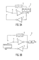
- FIGS. 3A and 3B illustrate a physical random number generator 11 (hereinafter "PRNG 11") as one embodiment of PRNG 10 ( FIG. 1 ).
- the PRNG 11 comprises a switching device in the form of an electronic switch 21 of a single pole/double throw switch variety (hereinafter "SPDT 21"), an oscillator in the form of a delay element 31 and an inverter 32, and a bi-stable latch in the form of the inverter 32 and an inverter 41.
- SPD1 21 is in a first operating state as shown in FIG.
- an output of the inverter 41 is disconnected from the input of the inverter 32 (i.e., the bi-stable latch is deactivated), and the delay element 31 and the inverter 32 are activated to generate the voltage oscillating signal V OS for conditionally provoking the inverters 32 and 41 into a metastable state upon a connection of the output of the inverter 41 to the input of the inverter 32.
- the SPDT 21 is in a second operating state as shown in FIG. 3B
- an output of the delay element 31 is disconnected from the input of the inverter 32 (i.e., the oscillator is deactivated), and the inverters 32 and 41 are activated to receive the voltage oscillating signal V OS and to latch the random number bit RNB.
- a logic voltage level V RNB of the random number bit RNB will reflect, after a delay, a stabilization of the unpredictable logic voltage level of the voltage oscillating signal V OS to a zero or an one. Otherwise, the logic voltage level V RNB of the random number bit RNB will follow the unpredictable logic voltage level of the voltage oscillating signal V OS , which will either be a zero or a one.
- the transition of the SPDT 21 between the first operating state and the second operating state occurs at a frequency (fixed or variable) and a duty cycle (fixed or variable) in accordance with an operational specification for the frequency and the duty cycle of a generation of the random number bit RNB.
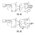
- FIGS. 4A and 4B illustrate a physical random number generator 12 (hereinafter "PRNG 12") as another embodiment of PRNG 10 ( FIG. 1 ).
- the PRNG 12 comprises a switching device in the form of a clock 22, a D-type flip-flop 23 (hereinafter “flip-flop 23”), and a pair of electronic switches 24 and 25 of a single pole/single throw switches variety (hereinafter "SPST 24" and “SPST 25”)(e.g. bi-directional analog CMOS switches in the form of anti-parallel FETs).
- SPST 24 single pole/single throw switches variety
- Other types of flip-flops can be substituted for flip-flop 23, and such substitutions can incorporate logic circuitry to create opposing outputs.
- the PRNG 12 further comprises the delay element 31, the inverter 32, and the inverter 41.
- Clock 22 and flip-flop 23 operate to cyclically transition SPST 24 and SPST 25 between an open position and a closed position in an opposing manner.
- the SPST 24 is in a closed position and SPST 25 is in an open position (i.e., the first operating state) in response to the clock signal CS being at a high logic voltage level (e.g., V HL of FIG. 1 ).
- the output of the inverter 41 is disconnected from the input of the inverter 32 (i.e., the bi-stable latch is deactivated), and the delay element 31 and the inverter 32 are activated to generate the voltage oscillating signal V OS for conditionally provoking the inverters 32 and 41 into a metastable state upon an activation ofbi-stable latch.
- the SPST 24 is in an open position and SPST 25 is in a closed position (i.e., the second operating state) in response to the clock signal CS being at a low logic voltage level (e.g., V LL of FIG. 1 ).
- the output of the delay element 31 is disconnected from the input of the inverter 32 (i.e., the oscillator is deactivated), and the inverters 32 and 41 are activated to receive the voltage oscillating signal V OS and to latch the random number bit RNB.
- a logic voltage level V RNB of the random number bit RNB will reflect, after a delay, a stabilization of the unpredictable logic voltage level of the voltage oscillating signal V OS to a zero or an one. Otherwise, the logic voltage level V RNB of the random number bit RNB will follow the unpredictable logic voltage level of the voltage oscillating signal V OS , which will either be a zero or a one.
- the respective opening and closing of SPST 24 and SPST 25 occurs at a frequency (fixed or variable) and a duty cycle (fixed or variable) of the clock signal CS, which is in accordance with an operational specification for the frequency and the duty cycle of a generation of the random number bit RNB.
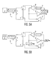
- FIGS. 5A and 5B illustrate a physical random number generator 13 (hereinafter "PRNG 13") as another embodiment of PRNG 10 ( FIG. 1 ).
- PRNG 13 comprises a switching device in the form of the clock 22 and the flip-flop 23. Again, other types of flip-flops can be substituted for flip-flop 23, and such substitutions can incorporate logic circuitry to create opposing outputs.
- the PRNG 13 further comprises an oscillator in the form of the delay element 31, the inverter 32, and a tri-state buffer 33, and a bi-stable latch in the form of the inverter 32 and an inverter 42.
- Clock 22 and flip-flop 23 operate to cyclically transition buffer 33 and inverter 42 between an ON state and an OFF state, when their output is of high impedance, in an opposing manner.
- the buffer 33 is in an ON state and the inverter 42 is in an OFF state in response to the clock signal CS being at a high logic voltage level (e.g., V HL of FIG. 1 ).
- V HL a high logic voltage level
- the output of the inverter 42 is disconnected from the input of the inverter 32 (i.e., the bi-stable latch is deactivated), and the delay element 31, the inverter 32 and the buffer 33 are activated to generate the voltage oscillating signal V OS for conditionally provoking the inverters 32 and 42 into a metastable state upon an activation of the inverters 32 and 42.
- the buffer 33 is in an OFF state and the inverter 42 is in an ON state in response to the clock signal CS being at a low logic voltage level (e.g., V LL of FIG. 1 ).
- V LL logic voltage level
- the buffer 33 is in the OFF state and inverter 42 is the ON state as shown in FIG. 5B , the output of the buffer 33 is disconnected from the input of the inverter 32 (i.e., the oscillator is deactivated), and the inverters 32 and 42 are activated to receive the voltage oscillating signal V OS and to latch the random number bit RNB.
- a logic voltage level V RNB of the random number bit RNB will reflect, after a delay, a stabilization of the unpredictable logic voltage level of the voltage oscillating signal V OS to a zero or an one. Otherwise, the logic voltage level V RNB of the random number bit RNB will follow the unpredictable logic voltage level of the voltage oscillating signal V OS , which will either be a zero or a one.
- the respective transition of the buffer 33 and the inverter 42 between the ON and OFF states occurs at a frequency (fixed or variable) and a duty cycle (fixed or variable) of the clock signal CS, which is in accordance with an operational specification for the frequency and the duty cycle of a generation of the random number bit RNB.
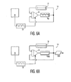
- FIGS. 6A and 6B illustrate a physical random number generator 14 (hereinafter "PRNG 14") as another embodiment of PRNG 10 ( FIG. 1 ).
- the PRNG 14 comprises the switching device 20, the delay element 31 and a multiplexer 34.
- the switching device 20 provides a switching signal SS to the multiplexer 34 for selecting either an illustrated inverting input of the multiplexer 34 to operate the delay element 31 and the multiplexer 34 as the oscillator (i.e., the first operating state) or an illustrated non-inverting input of the multiplexer 34 to operate the multiplexer 34 as the bi-stable latch (i.e., the second operating state).
- a frequency (fixed or variable) and a duty cycle (fixed or variable) of the switching signal SS is in accordance with an operational specification for the frequency and the duty cycle of a generation of the random number bit RNB.
- the negative feedback of the output of the multiplexer 34 through the delay element 31 to the inverting input of the multiplexer 34 forms a ring oscillator whereby the voltage oscillating signal V OS is generated as illustrated in FIG. 6A .
- the feedback from the output of the multiplexer 34 to the non-inverting input of the multiplexer 34 forms a bi-stable latch whereby the random number bit RNB having a logic voltage level V RNB is latched as illustrated in FIG. 6B .
- the logic voltage level of the oscillator is unpredictable due to the phase noise and frequency drift resulted from the internal noise of the oscillator.
- the bi-stable latch When the unpredictable logic voltage level of voltage oscillating signal V OS is within the indeterminate range of the bi-stable latch, the bi-stable latch is provoked into a metastable state whereby the logic voltage level V RNB of the random number bit will stabilize after a delay to either a zero or a one. Otherwise, the logic voltage level V RNB will follow the unpredictable logic voltage level of the voltage oscillating signal V OS as a zero or a one.
- the resulting random number bit RNB is preferably read at the next switch change, when the bi-stable latch is deactivated and the ring oscillator is formed again with the delay element 31.
- FIGS. 7A and 7B illustrate a physical random number generator 15 (hereinafter "PRNG 15") as another embodiment of PRNG 10 ( FIG. 1 ).
- the PRNG 15 comprises the switching device 20, the delay element 31 and an XOR gate 35.
- the switching device 20 provides a switching signal SS to a first input of the XOR gate 35 at the high logic voltage level V HL ( FIG. 1 ) to operate the delay element 31 and the XOR gate 35 as the oscillator (i.e., the first operating state) or at the low logic voltage level V LL ( FIG. 1 ) to operate XOR gate 35 as the bi-stable latch (i.e., the second operating state).
- a frequency (fixed or variable) and a duty cycle (fixed or variable) of the switching signal SS is in accordance with an operational specification for the frequency and the duty cycle of a generation of the random number bit RNB.
- the switching signal is at the high logic voltage level V HL , (i.e., the oscillator is activated and the bi-stable latch is deactivated)
- the feedback of the output of the XOR gate 35 through the delay element 31 to a second input of the XOR gate 35 forms a ring oscillator whereby the voltage oscillating signal V OS is generated as illustrated in FIG. 7A .
- the feedback of the output of the XOR gate 35 through the delay element 31 to the second input of the XOR gate 35 forms a bi-stable latch whereby the random number bit RNB having a logic voltage level V RNB is latched as illustrated in FIG. 6B .
- the logic voltage level of the oscillator is unpredictable due to the phase noise and frequency drift resulted from the internal noise of the oscillator.
- the bi-stable latch When the unpredictable logic voltage level of voltage oscillating signal V OS is within the indeterminate range of the bi-stable latch, the bi-stable latch is provoked into a metastable state whereby the logic voltage level V RNB of the random number bit will stabilize after a delay to either a zero or a one. Otherwise, the logic voltage level V RNB will follow the unpredictable logic voltage level of the voltage oscillating signal V OS as a zero or a one.
- the resulting random number bit RNB is preferably read at the next switch change, when the bi-stable latch is deactivated and the ring oscillator is formed again with the delay element 31.
- FIG. 8 illustrates a physical random number generating system 50 employing a plurality of PRNG 10 1 -10 X electrically coupled to logic circuit 51 (e.g., a multi-input XOR gate) to thereby provide a plurality of random number bits RNB 1 -RNB X to the logic circuit 51.
- logic circuit 51 e.g., a multi-input XOR gate
- the logic circuit 51 will provide a system random number bit SRNB that is sufficiently insensitive to any of the plurality of PRNG 10 1 -10 X producing corresponding random number bits RNB 1 -RNB X as a constant bit stream. As long as any one of the PRNG 10 1 -10 X produces random bits, the resulting system random number bit SRNB will also be random. On a VLSI chip, integrating several hundreds of slightly different PRNG 10 X is feasible and the resulting bit stream will be highly unpredictable.
- One benefit of the present invention is the facilitation of an easy implementation of a low power and relatively inexpensive physical random noise generator.
Landscapes
- Stabilization Of Oscillater, Synchronisation, Frequency Synthesizers (AREA)
- Semiconductor Integrated Circuits (AREA)
- Control Of Charge By Means Of Generators (AREA)
- Control Of Eletrric Generators (AREA)
- Oscillators With Electromechanical Resonators (AREA)
- Inductance-Capacitance Distribution Constants And Capacitance-Resistance Oscillators (AREA)
- Memory System Of A Hierarchy Structure (AREA)
Claims (14)
- Physischer Zufallszahlengenerator (10), umfassend:einen Oszillator (30), der betriebsfähig ist, um selektiv aktiviert und deaktiviert zu werden; undeinen bistabilen Latch (40), der betriebsfähig ist, um selektiv aktiviert und deaktiviert zu werden,wobei der Oszillator (30) aktiviert ist, um ein Spannungsoszillationssignal (VOS) zu erzeugen, wobei das Spannungsoszillationssignal (VOS) einen nicht vorhersagbaren logischen Spannungspegel aufweist, und wobei, wenn der Oszillator (30) deaktiviert ist, der bistabile Latch (40) aktiviert ist, um das Spannungsoszillationssignal (VOS) zu empfangen und in Abhängigkeit von dem nicht vorhersagbaren logischen Spannungspegel des Spannungsoszillationssignals (VOS) eine Zufallsbitzahl (RNB) zu einer Zeit des Empfangs des Spannungsoszillationssignals (VOS) durch den bistabilen Latch (40) zu speichern.
- Physischer Zufallszahlengenerator (10) nach Anspruch 1, ferner umfassend eine Schaltvorrichtung (20), die betriebsfähig ist, um zwischen einem ersten Betriebszustand und einem zweiten Betriebszustand überzugehen, wobei der bistabile Latch (40) deaktiviert ist und der Oszillator (30) aktiviert ist, wenn die Schaltvorrichtung (20) in dem ersten Betriebszustand betrieben wird, und wobei der Oszillator (30) deaktiviert ist und der bistabile Latch (40) aktiviert ist, wenn die Schaltvorrichtung (20) in dem zweiten Betriebszustand betrieben wird.
- Physischer Zufallszahlengenerator (10) nach Anspruch 2, wobei die Schaltvorrichtung (20) ein elektronischer Latch (21) ist, der betriebsfähig ist, um zwischen dem ersten Betriebszustand und dem zweiten Betriebszustand überzugehen, und wobei der Oszillator (30) ein Verzögerungselement (31) und einen Inverter (32) enthält, die betriebsfähig sind, um gleichzeitig aktiviert zu werden, wenn der elektronische Schalter (21) in dem ersten Betriebszustand betrieben wird.
- Physischer Zufallszahlengenerator (10) nach Anspruch 2, wobei die Schaltvorrichtung (20) einen Schalter (21) enthält, der betriebsfähig ist, um zwischen dem ersten Betriebszustand und dem zweiten Betriebszustand überzugehen, und wobei der bistabile Latch einen ersten Inverter (32) und einen zweiten Inverter (41) enthält, die betriebsfähig sind, um gleichzeitig aktiviert zu werden, wenn der elektronische Schalter (21) in dem ersten Betriebszustand betrieben wird.
- Physischer Zufallszahlengenerator (10) nach Anspruch 2, wobei die Schaltvorrichtung (20) einen ersten elektronischen Schalter (24), der betriebsfähig ist, um in dem ersten Betriebszustand geschlossen zu werden und in dem zweiten Betriebszustand geöffnet zu werden, und einen zweiten elektronischen Schalter (25), der betriebsfähig ist, um in dem ersten Betriebszustand geöffnet zu werden und in dem zweiten Betriebszustand geschlossen zu werden, einen Taktgeber (22), der betriebsfähig ist, um ein Taktsignal (CS) bereitzustellen, und einen Flip-Flop (23) enthält, der betriebsfähig ist, um den ersten elektronischen Schalter (24) und den zweiten elektronischen Schalter (25) in Reaktion auf das Taktsignal (CS) abwechselnd zu schließen und zu öffnen.
- Physischer Zufallszahlengenerator (10) nach Anspruch 5, wobei der Oszillator (30) ein Verzögerungselement (31) und einen Inverter (32) enthält, die betriebsfähig sind, um gleichzeitig aktiviert zu werden, wenn der erste elektronische Schalter (24) geschlossen ist.
- Physischer Zufallszahlengenerator (10) nach Anspruch 5, wobei der bistabile Latch einen ersten Inverter (32) und einen zweiten Inverter (41) enthält, die betriebsfähig sind, um gleichzeitig aktiviert zu werden, wenn der zweite elektronische Schalter (25) geschlossen ist.
- Physischer Zufallszahlengenerator (10) nach Anspruch 2, wobei der Oszillator (30) ein Verzögerungselement (31), einen Inverter (32) und einen Puffer (33) enthält, und wobei die Schaltvorrichtung (20) einen Taktgeber (22), der betriebsfähig ist, um ein Taktsignal (CS) bereitzustellen, und einen Flip-Flop (23) enthält, der betriebsfähig ist, um gemeinsam das Verzögerungselement (31), den Inverter (32) und den Puffer (33) in Reaktion darauf zu aktivieren, dass das Taktsignal (CS) einen den ersten Betriebszustand repräsentierenden Spannungspegel aufweist.
- Physischer Zufallszahlengenerator (10) nach Anspruch 2, wobei der Oszillator (30) einen ersten Inverter (32) und einen zweiten Inverter (42) enthält, und wobei die Schaltvorrichtung (20) einen Taktgeber (22), der betriebsfähig ist, um ein Taktsignal (CS) bereitzustellen, und einen Flip-Flop (23) enthält, der betriebsfähig ist, um gemeinsam den ersten Inverter (32) und den zweiten Inverter (42) in Reaktion darauf zu aktivieren, dass das Taktsignal (CS) einen den zweiten Betriebszustand repräsentierenden Spannungspegel aufweist.
- Physischer Zufallszahlengenerator (10) nach Anspruch 1, wobei der Oszillator (30) einen Multiplexer (34) und ein Verzögerungselement (31) enthält, das betriebsfähig ist, um Feedback von einem Ausgang des Multiplexers (34) an einen invertierenden Eingang des Multiplexers (34) bereitzustellen.
- Physischer Zufallszahlengenerator (10) nach Anspruch 1, wobei der bistabile Latch (40) einen Multiplexer (34) enthält, der betriebsfähig ist, um Feedback von einem Ausgang des Multiplexers (34) an einen nicht-invertierenden Eingang des Multiplexers (34) bereitzustellen.
- Physischer Zufallszahlengenerator (10) nach Anspruch 1, wobei der Oszillator (30) ein XOR-Gatter (35) und ein Verzögerungselement (31) enthält, das betriebsfähig ist, um Feedback von einem Ausgang des Multiplexers (34) an einen Eingang des Multiplexers (34) bereitzustellen.
- Physischer Zufallszahlengenerator (10) nach Anspruch 1, wobei der bistabile Latch (30) ein XOR-Gatter (35) und ein Verzögerungselement (31) enthält, das betriebsfähig ist, um Feedback von einem Ausgang des Multiplexers (34) an einen Eingang des Multiplexers (34) bereitzustellen.
- Physisches Zufallszahlengenerierungssystem (50), umfassend:eine Vielzahl von Zufallszahlengeneratoren (101, ..., 10X), die betriebsfähig sind, um eine Vielzahl von Zufallszahlenbits (RNB1,... , RNBX) bereitzustellen, eine logische Schaltung (51), die betriebsfähig ist, um ein Systemzufallszahlenbit (SRNB) in Reaktion auf den Empfang der Vielzahl von Zufallszahlenbit (RNB1, ..., RNBX) bereitzustellen, und wobei ein erster Zufallszahlengenerator (101, ..., 10X) ein Zufallszahlengenerator (101, ..., 10X) nach einem der Ansprüche 1 bis 13 ist.
Applications Claiming Priority (3)
| Application Number | Priority Date | Filing Date | Title |
|---|---|---|---|
| US10/205,273 US6771104B2 (en) | 2002-07-25 | 2002-07-25 | Switching electronic circuit for random number generation |
| US205273 | 2002-07-25 | ||
| PCT/IB2003/003235 WO2004012334A2 (en) | 2002-07-25 | 2003-07-14 | Switching electronic circuit for random number generation |
Publications (2)
| Publication Number | Publication Date |
|---|---|
| EP1543407A2 EP1543407A2 (de) | 2005-06-22 |
| EP1543407B1 true EP1543407B1 (de) | 2008-02-13 |
Family
ID=30770037
Family Applications (1)
| Application Number | Title | Priority Date | Filing Date |
|---|---|---|---|
| EP03771230A Expired - Lifetime EP1543407B1 (de) | 2002-07-25 | 2003-07-14 | Abtastschaltkreis zur zufallszahlengenerierung |
Country Status (8)
| Country | Link |
|---|---|
| US (1) | US6771104B2 (de) |
| EP (1) | EP1543407B1 (de) |
| JP (1) | JP2005534249A (de) |
| CN (1) | CN1672127B (de) |
| AT (1) | ATE386292T1 (de) |
| AU (1) | AU2003247074A1 (de) |
| DE (1) | DE60319104T2 (de) |
| WO (1) | WO2004012334A2 (de) |
Families Citing this family (22)
| Publication number | Priority date | Publication date | Assignee | Title |
|---|---|---|---|---|
| US7047262B2 (en) * | 2002-08-21 | 2006-05-16 | Koninklijke Philips Electronics N.V. | Entropy estimation and decimation for improving the randomness of true random number generation |
| US7325021B2 (en) * | 2003-03-14 | 2008-01-29 | Nxp B.V. | VLSI implementation of metastability-based random number generator using delay ladders |
| KR20060095942A (ko) * | 2004-11-18 | 2006-09-05 | 가부시키가이샤 니이가타 티엘오 | 난수 생성 방법 및 난수 생성 장치 |
| US7634522B1 (en) | 2004-11-30 | 2009-12-15 | Novell, Inc. | Random number generation |
| WO2007019244A2 (en) * | 2005-08-03 | 2007-02-15 | Nano-Proprietary, Inc. | Continuous range hydrogen sensor |
| US8346832B2 (en) * | 2006-10-12 | 2013-01-01 | The Regents Of The University Of Michigan | Random number generator |
| US8583712B2 (en) * | 2007-09-18 | 2013-11-12 | Seagate Technology Llc | Multi-bit sampling of oscillator jitter for random number generation |
| KR101579837B1 (ko) * | 2009-02-09 | 2015-12-24 | 삼성전자주식회사 | 난수 발생 장치 및 난수 발생 방법 |
| US8886692B2 (en) * | 2009-02-09 | 2014-11-11 | Samsung Electronics Co., Ltd. | Apparatus for generating random number |
| US20100281088A1 (en) * | 2009-04-29 | 2010-11-04 | Psigenics Corporation | Integrated true random number generator |
| KR20110060033A (ko) * | 2009-11-30 | 2011-06-08 | 박옥희 | 해상 구조물용 커플링 |
| US20110191129A1 (en) * | 2010-02-04 | 2011-08-04 | Netzer Moriya | Random Number Generator Generating Random Numbers According to an Arbitrary Probability Density Function |
| US8285767B2 (en) | 2011-03-07 | 2012-10-09 | Arm Limited | Apparatus and method for generating a random number |
| US8788551B2 (en) | 2011-11-15 | 2014-07-22 | Seagate Technology Llc | Random number generation using switching regulators |
| US9201630B2 (en) | 2012-02-10 | 2015-12-01 | Seagate Technology Llc | Random number generation using startup variances |
| US10141930B2 (en) * | 2013-06-04 | 2018-11-27 | Nvidia Corporation | Three state latch |
| JP6167876B2 (ja) * | 2013-11-28 | 2017-07-26 | 富士通株式会社 | 電子回路、電子機器及び認証システム |
| US9189202B2 (en) * | 2013-12-23 | 2015-11-17 | The University Of Massachusetts | Generate random numbers using metastability resolution time |
| US9774317B1 (en) | 2016-08-29 | 2017-09-26 | Amazon Technologies, Inc. | Bistable-element for random number generation |
| WO2019030667A1 (en) * | 2017-08-08 | 2019-02-14 | Politechnika Warszawska | RANDOM NUMBER GENERATOR |
| CN109656514B (zh) | 2017-10-11 | 2023-08-15 | 华邦电子股份有限公司 | 随机数产生系统及其随机数产生方法 |
| TWI634479B (zh) * | 2017-10-11 | 2018-09-01 | 華邦電子股份有限公司 | 隨機數產生系統及其隨機數產生方法 |
Citations (2)
| Publication number | Priority date | Publication date | Assignee | Title |
|---|---|---|---|---|
| EP0365930A2 (de) * | 1988-10-28 | 1990-05-02 | International Business Machines Corporation | Zufallszahlenerzeugungsschaltung |
| US5963104A (en) * | 1996-04-15 | 1999-10-05 | Vlsi Technology, Inc. | Standard cell ring oscillator of a non-deterministic randomizer circuit |
Family Cites Families (20)
| Publication number | Priority date | Publication date | Assignee | Title |
|---|---|---|---|---|
| US3866128A (en) * | 1973-06-25 | 1975-02-11 | Nasa | Random pulse generator |
| US4395703A (en) * | 1981-06-29 | 1983-07-26 | Motorola Inc. | Precision digital random data generator |
| US4571556A (en) | 1983-07-28 | 1986-02-18 | Mi Medical & Scientific Instruments, Inc. | Randomized-clock circuit |
| US4810975A (en) * | 1987-08-10 | 1989-03-07 | Dallas Semiconductor Corp. | Random number generator using sampled output of variable frequency oscillator |
| US5153532A (en) | 1989-05-24 | 1992-10-06 | Honeywell Inc. | Noise generator using combined outputs of two pseudo-random sequence generators |
| DE4302830C1 (de) | 1993-01-27 | 1994-03-03 | Siemens Ag | Rückgekoppeltes Schieberegister zum Erzeugen von Pseudozufallszahlenfolgen darstellenden digitalen Signalen |
| US5606322A (en) | 1994-10-24 | 1997-02-25 | Motorola, Inc. | Divergent code generator and method |
| US5570307A (en) | 1995-01-06 | 1996-10-29 | Vlsi Technology, Inc. | Digital randomizer for on-chip generation and storage of random self-programming data block |
| US6324558B1 (en) | 1995-02-14 | 2001-11-27 | Scott A. Wilber | Random number generator and generation method |
| JP3410269B2 (ja) | 1995-12-21 | 2003-05-26 | 株式会社アドバンテスト | 遅延時間測定方法 |
| US5706218A (en) * | 1996-05-15 | 1998-01-06 | Intel Corporation | Random number generator |
| US5961577A (en) * | 1996-12-05 | 1999-10-05 | Texas Instruments Incorporated | Random binary number generator |
| GB2333652A (en) | 1998-01-24 | 1999-07-28 | Motorola Ltd | Random number generator with improved equiprobability |
| US6065029A (en) * | 1998-05-26 | 2000-05-16 | N*Able Technologies, Inc. | Method and system for providing a random number generator |
| US6046616A (en) | 1998-08-07 | 2000-04-04 | Tritech Microelectronics, Ltd. | Two dimensional random pulse generator |
| JP2000066592A (ja) | 1998-08-19 | 2000-03-03 | Syst Kogaku Kk | 乱数生成装置 |
| GB2353155A (en) | 1999-08-05 | 2001-02-14 | Mitsubishi Electric Inf Tech | A random binary signal generator with a narrowed autocorrelation function |
| EP1111784B1 (de) | 1999-12-22 | 2008-07-30 | Telefonaktiebolaget LM Ericsson (publ) | Verfahren und elektrische Vorrichtung für die leistungsfähige Generierung von Mehrfachraten-Pseudozufallsfolgen |
| US6522210B1 (en) | 2000-02-16 | 2003-02-18 | Honeywell International Inc. | Random pulse generator |
| US6480072B1 (en) * | 2000-04-18 | 2002-11-12 | Advanced Micro Devices, Inc. | Method and apparatus for generating random numbers |
-
2002
- 2002-07-25 US US10/205,273 patent/US6771104B2/en not_active Expired - Fee Related
-
2003
- 2003-07-14 AU AU2003247074A patent/AU2003247074A1/en not_active Abandoned
- 2003-07-14 CN CN03817550.9A patent/CN1672127B/zh not_active Expired - Fee Related
- 2003-07-14 EP EP03771230A patent/EP1543407B1/de not_active Expired - Lifetime
- 2003-07-14 WO PCT/IB2003/003235 patent/WO2004012334A2/en not_active Ceased
- 2003-07-14 JP JP2004524020A patent/JP2005534249A/ja active Pending
- 2003-07-14 AT AT03771230T patent/ATE386292T1/de not_active IP Right Cessation
- 2003-07-14 DE DE60319104T patent/DE60319104T2/de not_active Expired - Lifetime
Patent Citations (2)
| Publication number | Priority date | Publication date | Assignee | Title |
|---|---|---|---|---|
| EP0365930A2 (de) * | 1988-10-28 | 1990-05-02 | International Business Machines Corporation | Zufallszahlenerzeugungsschaltung |
| US5963104A (en) * | 1996-04-15 | 1999-10-05 | Vlsi Technology, Inc. | Standard cell ring oscillator of a non-deterministic randomizer circuit |
Non-Patent Citations (1)
| Title |
|---|
| PETRIE C.S.; CONNELLY J.A.: "Modeling and Simulation of Oscillator-Based Random Number Generators", IEEE, vol. 4, 12 May 1996 (1996-05-12), NEW YORK, IEEE, US, pages 324 - 327, XP000618584 * |
Also Published As
| Publication number | Publication date |
|---|---|
| JP2005534249A (ja) | 2005-11-10 |
| WO2004012334A3 (en) | 2004-05-21 |
| ATE386292T1 (de) | 2008-03-15 |
| DE60319104D1 (de) | 2008-03-27 |
| CN1672127A (zh) | 2005-09-21 |
| EP1543407A2 (de) | 2005-06-22 |
| US20040017235A1 (en) | 2004-01-29 |
| CN1672127B (zh) | 2010-08-18 |
| US6771104B2 (en) | 2004-08-03 |
| DE60319104T2 (de) | 2009-02-05 |
| AU2003247074A8 (en) | 2004-02-16 |
| WO2004012334A2 (en) | 2004-02-05 |
| AU2003247074A1 (en) | 2004-02-16 |
Similar Documents
| Publication | Publication Date | Title |
|---|---|---|
| US6771104B2 (en) | Switching electronic circuit for random number generation | |
| US7868677B2 (en) | Low power flip-flop circuit | |
| US8341201B2 (en) | Random number generator | |
| CN109314506B (zh) | 低时钟功率数据门控触发器 | |
| EP1527384B1 (de) | Speicherschaltkreis zur zufallszahlengenerierung | |
| KR100394841B1 (ko) | 데이터 래치 회로와 그 구동 방법 | |
| KR100612417B1 (ko) | 펄스-기반 고속 저전력 게이티드 플롭플롭 회로 | |
| US7315874B2 (en) | Electronic circuit for random number generation | |
| US6864735B2 (en) | Circuit and method for regenerating reset and clock signals and high-speed digital system incorporating the same | |
| EP1776757A1 (de) | Zufallszahlengenerator auf der basis von logikschaltungen mit rückkopplung | |
| US20080074151A1 (en) | Dual-edge-triggered, clock-gated logic circuit and method | |
| US7710208B2 (en) | Multi-speed ring oscillator | |
| KR960018901A (ko) | 피이드백 래치 및 피이드백 래치의 피이드백 동작 형성 방법 | |
| US7873896B2 (en) | High performance pulsed storage circuit | |
| WO1993023804A1 (en) | Apparatus and method for random number generation | |
| US7132870B2 (en) | Differential register slave structure | |
| US6597211B2 (en) | Clock divider circuit producing 0° and 90° outputs with a 50% duty cycle | |
| US9602085B2 (en) | Data storage element and signal processing method | |
| CN222690378U (zh) | 数据存储结构、芯片及电子设备 | |
| US11652485B2 (en) | Analog hashing engines using physical dynamical systems | |
| KR100294972B1 (ko) | 수정발진회로 | |
| CN121879719A (zh) | 真随机数发生器、真随机数产生方法、芯片及电子设备 | |
| Turaga et al. | Power reduction technique using adiabatic logic | |
| KR20010055156A (ko) | 마이크로 컨트롤러의 동작 모드 선택 회로 | |
| JP2000216668A (ja) | 波形整形回路 |
Legal Events
| Date | Code | Title | Description |
|---|---|---|---|
| PUAI | Public reference made under article 153(3) epc to a published international application that has entered the european phase |
Free format text: ORIGINAL CODE: 0009012 |
|
| 17P | Request for examination filed |
Effective date: 20050225 |
|
| AK | Designated contracting states |
Kind code of ref document: A2 Designated state(s): AT BE BG CH CY CZ DE DK EE ES FI FR GB GR HU IE IT LI LU MC NL PT RO SE SI SK TR |
|
| AX | Request for extension of the european patent |
Extension state: AL LT LV MK |
|
| RIN1 | Information on inventor provided before grant (corrected) |
Inventor name: HARS, LASZLO |
|
| DAX | Request for extension of the european patent (deleted) | ||
| GRAP | Despatch of communication of intention to grant a patent |
Free format text: ORIGINAL CODE: EPIDOSNIGR1 |
|
| RAP1 | Party data changed (applicant data changed or rights of an application transferred) |
Owner name: NXP B.V. |
|
| GRAS | Grant fee paid |
Free format text: ORIGINAL CODE: EPIDOSNIGR3 |
|
| GRAA | (expected) grant |
Free format text: ORIGINAL CODE: 0009210 |
|
| AK | Designated contracting states |
Kind code of ref document: B1 Designated state(s): AT BE BG CH CY CZ DE DK EE ES FI FR GB GR HU IE IT LI LU MC NL PT RO SE SI SK TR |
|
| REG | Reference to a national code |
Ref country code: GB Ref legal event code: FG4D |
|
| REG | Reference to a national code |
Ref country code: CH Ref legal event code: EP |
|
| REG | Reference to a national code |
Ref country code: IE Ref legal event code: FG4D |
|
| REF | Corresponds to: |
Ref document number: 60319104 Country of ref document: DE Date of ref document: 20080327 Kind code of ref document: P |
|
| PG25 | Lapsed in a contracting state [announced via postgrant information from national office to epo] |
Ref country code: FI Free format text: LAPSE BECAUSE OF FAILURE TO SUBMIT A TRANSLATION OF THE DESCRIPTION OR TO PAY THE FEE WITHIN THE PRESCRIBED TIME-LIMIT Effective date: 20080213 Ref country code: ES Free format text: LAPSE BECAUSE OF FAILURE TO SUBMIT A TRANSLATION OF THE DESCRIPTION OR TO PAY THE FEE WITHIN THE PRESCRIBED TIME-LIMIT Effective date: 20080524 |
|
| NLV1 | Nl: lapsed or annulled due to failure to fulfill the requirements of art. 29p and 29m of the patents act | ||
| PG25 | Lapsed in a contracting state [announced via postgrant information from national office to epo] |
Ref country code: AT Free format text: LAPSE BECAUSE OF FAILURE TO SUBMIT A TRANSLATION OF THE DESCRIPTION OR TO PAY THE FEE WITHIN THE PRESCRIBED TIME-LIMIT Effective date: 20080213 |
|
| ET | Fr: translation filed | ||
| PG25 | Lapsed in a contracting state [announced via postgrant information from national office to epo] |
Ref country code: SI Free format text: LAPSE BECAUSE OF FAILURE TO SUBMIT A TRANSLATION OF THE DESCRIPTION OR TO PAY THE FEE WITHIN THE PRESCRIBED TIME-LIMIT Effective date: 20080213 Ref country code: BE Free format text: LAPSE BECAUSE OF FAILURE TO SUBMIT A TRANSLATION OF THE DESCRIPTION OR TO PAY THE FEE WITHIN THE PRESCRIBED TIME-LIMIT Effective date: 20080213 |
|
| PG25 | Lapsed in a contracting state [announced via postgrant information from national office to epo] |
Ref country code: CZ Free format text: LAPSE BECAUSE OF FAILURE TO SUBMIT A TRANSLATION OF THE DESCRIPTION OR TO PAY THE FEE WITHIN THE PRESCRIBED TIME-LIMIT Effective date: 20080213 Ref country code: DK Free format text: LAPSE BECAUSE OF FAILURE TO SUBMIT A TRANSLATION OF THE DESCRIPTION OR TO PAY THE FEE WITHIN THE PRESCRIBED TIME-LIMIT Effective date: 20080213 Ref country code: SE Free format text: LAPSE BECAUSE OF FAILURE TO SUBMIT A TRANSLATION OF THE DESCRIPTION OR TO PAY THE FEE WITHIN THE PRESCRIBED TIME-LIMIT Effective date: 20080513 Ref country code: NL Free format text: LAPSE BECAUSE OF FAILURE TO SUBMIT A TRANSLATION OF THE DESCRIPTION OR TO PAY THE FEE WITHIN THE PRESCRIBED TIME-LIMIT Effective date: 20080213 Ref country code: PT Free format text: LAPSE BECAUSE OF FAILURE TO SUBMIT A TRANSLATION OF THE DESCRIPTION OR TO PAY THE FEE WITHIN THE PRESCRIBED TIME-LIMIT Effective date: 20080714 Ref country code: SK Free format text: LAPSE BECAUSE OF FAILURE TO SUBMIT A TRANSLATION OF THE DESCRIPTION OR TO PAY THE FEE WITHIN THE PRESCRIBED TIME-LIMIT Effective date: 20080213 |
|
| PG25 | Lapsed in a contracting state [announced via postgrant information from national office to epo] |
Ref country code: RO Free format text: LAPSE BECAUSE OF FAILURE TO SUBMIT A TRANSLATION OF THE DESCRIPTION OR TO PAY THE FEE WITHIN THE PRESCRIBED TIME-LIMIT Effective date: 20080213 |
|
| PLBE | No opposition filed within time limit |
Free format text: ORIGINAL CODE: 0009261 |
|
| STAA | Information on the status of an ep patent application or granted ep patent |
Free format text: STATUS: NO OPPOSITION FILED WITHIN TIME LIMIT |
|
| 26N | No opposition filed |
Effective date: 20081114 |
|
| REG | Reference to a national code |
Ref country code: CH Ref legal event code: PL |
|
| PG25 | Lapsed in a contracting state [announced via postgrant information from national office to epo] |
Ref country code: MC Free format text: LAPSE BECAUSE OF NON-PAYMENT OF DUE FEES Effective date: 20080731 |
|
| PG25 | Lapsed in a contracting state [announced via postgrant information from national office to epo] |
Ref country code: BG Free format text: LAPSE BECAUSE OF FAILURE TO SUBMIT A TRANSLATION OF THE DESCRIPTION OR TO PAY THE FEE WITHIN THE PRESCRIBED TIME-LIMIT Effective date: 20080513 Ref country code: EE Free format text: LAPSE BECAUSE OF FAILURE TO SUBMIT A TRANSLATION OF THE DESCRIPTION OR TO PAY THE FEE WITHIN THE PRESCRIBED TIME-LIMIT Effective date: 20080213 |
|
| PG25 | Lapsed in a contracting state [announced via postgrant information from national office to epo] |
Ref country code: LI Free format text: LAPSE BECAUSE OF NON-PAYMENT OF DUE FEES Effective date: 20080731 Ref country code: CH Free format text: LAPSE BECAUSE OF NON-PAYMENT OF DUE FEES Effective date: 20080731 |
|
| PG25 | Lapsed in a contracting state [announced via postgrant information from national office to epo] |
Ref country code: IE Free format text: LAPSE BECAUSE OF NON-PAYMENT OF DUE FEES Effective date: 20080714 Ref country code: CY Free format text: LAPSE BECAUSE OF FAILURE TO SUBMIT A TRANSLATION OF THE DESCRIPTION OR TO PAY THE FEE WITHIN THE PRESCRIBED TIME-LIMIT Effective date: 20080213 |
|
| PG25 | Lapsed in a contracting state [announced via postgrant information from national office to epo] |
Ref country code: IT Free format text: LAPSE BECAUSE OF FAILURE TO SUBMIT A TRANSLATION OF THE DESCRIPTION OR TO PAY THE FEE WITHIN THE PRESCRIBED TIME-LIMIT Effective date: 20080213 |
|
| PG25 | Lapsed in a contracting state [announced via postgrant information from national office to epo] |
Ref country code: HU Free format text: LAPSE BECAUSE OF FAILURE TO SUBMIT A TRANSLATION OF THE DESCRIPTION OR TO PAY THE FEE WITHIN THE PRESCRIBED TIME-LIMIT Effective date: 20080814 Ref country code: LU Free format text: LAPSE BECAUSE OF NON-PAYMENT OF DUE FEES Effective date: 20080714 |
|
| PG25 | Lapsed in a contracting state [announced via postgrant information from national office to epo] |
Ref country code: TR Free format text: LAPSE BECAUSE OF FAILURE TO SUBMIT A TRANSLATION OF THE DESCRIPTION OR TO PAY THE FEE WITHIN THE PRESCRIBED TIME-LIMIT Effective date: 20080213 |
|
| PG25 | Lapsed in a contracting state [announced via postgrant information from national office to epo] |
Ref country code: GR Free format text: LAPSE BECAUSE OF FAILURE TO SUBMIT A TRANSLATION OF THE DESCRIPTION OR TO PAY THE FEE WITHIN THE PRESCRIBED TIME-LIMIT Effective date: 20080514 |
|
| PGFP | Annual fee paid to national office [announced via postgrant information from national office to epo] |
Ref country code: GB Payment date: 20120629 Year of fee payment: 10 |
|
| PGFP | Annual fee paid to national office [announced via postgrant information from national office to epo] |
Ref country code: FR Payment date: 20120806 Year of fee payment: 10 Ref country code: DE Payment date: 20120625 Year of fee payment: 10 |
|
| GBPC | Gb: european patent ceased through non-payment of renewal fee |
Effective date: 20130714 |
|
| REG | Reference to a national code |
Ref country code: DE Ref legal event code: R119 Ref document number: 60319104 Country of ref document: DE Effective date: 20140201 |
|
| REG | Reference to a national code |
Ref country code: FR Ref legal event code: ST Effective date: 20140331 |
|
| PG25 | Lapsed in a contracting state [announced via postgrant information from national office to epo] |
Ref country code: DE Free format text: LAPSE BECAUSE OF NON-PAYMENT OF DUE FEES Effective date: 20140201 Ref country code: GB Free format text: LAPSE BECAUSE OF NON-PAYMENT OF DUE FEES Effective date: 20130714 |
|
| PG25 | Lapsed in a contracting state [announced via postgrant information from national office to epo] |
Ref country code: FR Free format text: LAPSE BECAUSE OF NON-PAYMENT OF DUE FEES Effective date: 20130731 |