EP1540821B1 - Schaltungsanordnung zur mittelwertbildung - Google Patents
Schaltungsanordnung zur mittelwertbildung Download PDFInfo
- Publication number
- EP1540821B1 EP1540821B1 EP03798049A EP03798049A EP1540821B1 EP 1540821 B1 EP1540821 B1 EP 1540821B1 EP 03798049 A EP03798049 A EP 03798049A EP 03798049 A EP03798049 A EP 03798049A EP 1540821 B1 EP1540821 B1 EP 1540821B1
- Authority
- EP
- European Patent Office
- Prior art keywords
- signal
- input
- output
- circuit arrangement
- counter
- Prior art date
- Legal status (The legal status is an assumption and is not a legal conclusion. Google has not performed a legal analysis and makes no representation as to the accuracy of the status listed.)
- Expired - Lifetime
Links
- 238000012935 Averaging Methods 0.000 title claims description 14
- 230000000737 periodic effect Effects 0.000 description 5
- 238000005070 sampling Methods 0.000 description 4
- 230000005540 biological transmission Effects 0.000 description 3
- 238000010586 diagram Methods 0.000 description 3
- 235000009508 confectionery Nutrition 0.000 description 1
- 230000001419 dependent effect Effects 0.000 description 1
- 238000011161 development Methods 0.000 description 1
- 230000018109 developmental process Effects 0.000 description 1
- 238000000034 method Methods 0.000 description 1
- 238000004088 simulation Methods 0.000 description 1
- 230000002123 temporal effect Effects 0.000 description 1
Images
Classifications
-
- G—PHYSICS
- G01—MEASURING; TESTING
- G01D—MEASURING NOT SPECIALLY ADAPTED FOR A SPECIFIC VARIABLE; ARRANGEMENTS FOR MEASURING TWO OR MORE VARIABLES NOT COVERED IN A SINGLE OTHER SUBCLASS; TARIFF METERING APPARATUS; MEASURING OR TESTING NOT OTHERWISE PROVIDED FOR
- G01D1/00—Measuring arrangements giving results other than momentary value of variable, of general application
- G01D1/02—Measuring arrangements giving results other than momentary value of variable, of general application giving mean values, e.g. root means square values
-
- H—ELECTRICITY
- H03—ELECTRONIC CIRCUITRY
- H03K—PULSE TECHNIQUE
- H03K5/00—Manipulating of pulses not covered by one of the other main groups of this subclass
- H03K5/19—Monitoring patterns of pulse trains
-
- H—ELECTRICITY
- H03—ELECTRONIC CIRCUITRY
- H03K—PULSE TECHNIQUE
- H03K5/00—Manipulating of pulses not covered by one of the other main groups of this subclass
- H03K5/01—Shaping pulses
- H03K5/08—Shaping pulses by limiting; by thresholding; by slicing, i.e. combined limiting and thresholding
-
- H—ELECTRICITY
- H03—ELECTRONIC CIRCUITRY
- H03K—PULSE TECHNIQUE
- H03K5/00—Manipulating of pulses not covered by one of the other main groups of this subclass
- H03K5/01—Shaping pulses
- H03K5/08—Shaping pulses by limiting; by thresholding; by slicing, i.e. combined limiting and thresholding
- H03K5/082—Shaping pulses by limiting; by thresholding; by slicing, i.e. combined limiting and thresholding with an adaptive threshold
- H03K5/084—Shaping pulses by limiting; by thresholding; by slicing, i.e. combined limiting and thresholding with an adaptive threshold modified by switching, e.g. by a periodic signal or by a signal in synchronism with the transitions of the output signal
Definitions
- the invention relates to a circuit arrangement for averaging according to the preamble of claim 1.
- solenoid valves are known to be used to control an automatic transmission, which are controlled by a pulse width modulated current signal.
- the time average of the current is detected in order to optimize the control behavior of the solenoid valve within a controlled system can.
- a disadvantage of the known averaging by analog filters is, on the one hand, the settling time of such filters, so that the mean value is generally available only after a few periods of the pulse width modulation.
- the invention is therefore an object of the invention to provide a circuit arrangement that allows the fastest possible and accurate averaging.
- the object is achieved on the basis of a known circuit arrangement according to the preamble of claim 1 by the characterizing features of claim 1.
- the invention encompasses the general technical teaching between the signal input and the signal output of the circuit arrangement to provide a summer or averaging counter.
- the input signal to be evaluated is therefore preferably first digitized so that the averaging can take place without the dynamic problems of analog filters in the digital domain.
- the totalizer or counter is connected on the input side to a sigma-delta modulator, which subjects the input signal to be evaluated to sigma-delta modulation and supplies the signal modulated in this way to the summer or counter.
- sigma-delta modulators are, for example, NORSWORTHY / SCHREIER / TEMES: “Delta-Sigma Data Converters” (IEEE Press), from CANDY / TEMES: “Oversampling Delta-Sigma Data Converters: Theory, Design and Simulation” (IEEE Press) and from ENGELEN / PLASSCHE: “Bandpass Sigma Delta Modulators” (Kluwer Academic Publishers).
- the sigma-delta modulator should in this case operate at a clock rate or sampling rate that is greater than the Nyquist rate of the input signal, so that an oversampling takes place and no signal information of the input signal is lost.
- the counter preferably has a reset input to which a control signal is supplied, which is generated for example by a microcontroller.
- the control signal and the input signal to be evaluated are in a time constant Phase relationship to each other, so that the same time window of the input signal is always evaluated.
- the input signal and the clock signal of the sigma-delta modulator are in a temporally constant phase relationship with each other, so that the same time window of the input signal is always evaluated.
- the input signal for the sigma-delta modulator is therefore preferably derived from the clock signal to be evaluated, for which purpose a conventional microcontroller, for example, can be used.
- the sigma-delta modulator can be designed to be either analog or digital.
- the sigma-delta modulator preferably has on the input side an adder or a subtractor, an integrator and a comparator on the output side, wherein the output of the comparator is fed back in a feedback loop to an input of the adder or subtractor.
- the integrator of the sigma-delta modulator may be implemented as a first-order integrator, but higher-order integrators may also be used in the sigma-delta modulator, thereby advantageously achieving higher resolution.
- the comparator arranged on the output side in the sigma-delta modulator has a predetermined decision threshold, which preferably corresponds to a zero level of the input signal.
- the comparator When the decision threshold is exceeded, the comparator preferably outputs a positive level, whereas the comparator preferably outputs a negative level when the decision threshold is undershot.
- the output of the comparator in the feedback loop does not become fed back directly to the input of the adder or subtractor, but used to drive a switching element selectively switches a first reference signal or a second reference signal to the input of the adder or subtractor.
- the output signal of the comparator can have inaccuracies which are not fed back in this way and thus suppressed.
- the reference signals can be generated by reference signal sources with high accuracy and constancy, so that the accuracy of the averaging is increased by this indirect feedback.
- an analog / digital converter is provided which scans the analog input signal to be evaluated, converted into a digital signal and then directly or indirectly the summer or the counter fed. From the number of previous samples and the output of the summer or counter can then be determined in a simple manner, the time average of the input signal by the output of the summer is divided by the number of added samples.
- the analog-to-digital converter should also operate at a sample rate greater than the Nyquist rate of the input signal to over-sample and lose any signal information from the input signal.
- the clock frequency of the analog / digital converter is therefore preferably an integer multiple of the cutoff frequency of the input signal to be evaluated, with an oversampling factor of 16, 32 or 64 being advantageous in order to achieve a sufficient signal-to-noise ratio ,
- the summer preferably has a reset input to which a control signal is supplied, which is generated for example by a microcontroller.
- the control signal and the input signal to be evaluated are in a temporally constant phase relationship with one another, so that the same time window of the input signal is always evaluated.
- an output register is preferably provided on the output side, that temporarily stores the mean value until the next mean value has been calculated.
- the circuit arrangement according to the invention is preferably suitable for averaging in the case of current and voltage signals in motor vehicle technology.
- the input signal to be evaluated-as already indicated at the beginning- can be a current signal with which a solenoid valve is actuated.
- circuit arrangement according to the invention does not necessarily have to be designed as a separate circuit. Rather, it is also possible that the circuit arrangement according to the invention is part of a complex electronic circuit which, in addition to averaging, also fulfills other functions.
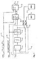
- the circuit arrangement shown in FIG. 1 can be used for example in an electronic transmission control of a motor vehicle in order to determine the time average of a current signal s.
- the circuit arrangement according to the invention has a signal input 1 to which the current signal s to be evaluated is applied.
- the signal input 1 is followed by a sigma-delta modulator 2, which is constructed analogously and consists of an adder 3, an integrator 4 and a comparator 5.
- the adder 3 has a non-inverting input, which is connected to the signal input 1 of the circuit arrangement according to the invention and receives the input signal s.
- the adder 3 has an inverting input, which can be selectively connected via a switching element 6 to one of two reference signal sources 7, 8.
- the reference signal source 7 generates a reference signal Neg_Ref with a negative polarity
- the reference signal source 8 generates a reference signal Pos_Ref with a positive polarity.
- the control of the switching element 6 takes place in dependence on the signal appearing at the output of the comparator 5.
- the switching element 6 has a control input which is connected to the output of the comparator 5.
- the switching element 6 connects the inverting input of the adder 3 to the reference signal source 8.
- the switching element 6 connects the inverting input of the adder 3 to the reference signal source 7.
- the adder 3 On the output side, the adder 3 is connected to the input of the integrator 4, wherein the integrator 4 is a first-order integrator in order to enable a simple circuit implementation.
- the integrator 4 is again connected on the output side to the comparator 5, which compares the output signal of the integrator 4 with a decision threshold which corresponds to a zero level of the input signal s.
- the comparator 5 When the decision threshold is exceeded, the comparator 5 outputs an output signal having a positive polarity, so that the switch 6 connects the inverting input of the adder 3 to the reference signal source 8.
- the comparator 6 when the decision threshold is undershot, the comparator 6 outputs an output signal having a negative polarity, so that the switch 6 connects the inverting input of the adder 3 to the reference signal source 7.
- the control of the switch 6 and a counter 10 by the comparator 5 is clock-controlled by a clock signal CLK, which is generated by a microcontroller and applied to a clock input 9.
- the clock frequency f CLK of the clock signal CLK is in this case 2 n times as large as the limit frequency f s of the band-limited input signal s, where n is an integer and greater than or equal to 1. This makes sense, so that an oversampling is given and no signal information is lost.
- the sigma-delta modulator 2 is connected to a release input ENABLE of the counter 10.
- a high level at the enable input ENABLE thus enables a counting process in which the counter reading in the counter 10 is incremented.
- the counter 10 has a clock input CLOCK, which is connected to the clock input 9 and thus also driven by the clock signal CLK.
- the counter has a reset input RESET, which is acted upon by a control signal CTRL, wherein the control signal CTRL is applied to a control input 11 and generated by a microcontroller.
- RESET reset input
- CTRL control signal
- the control signal CTRL is generated by the microcontroller, which always has a constant phase relationship between the input signal s and the control signal CTRL. In this way it is achieved that in each case the same time window of the periodic input signal s is evaluated, since the counter 10 is reset by the control signal CTRL.
- the count of the counter 10 thus reflects the time average of the input signal s during the current period of the pulse width modulation.
- the counter 10 On the output side, the counter 10 is connected to an output register 12, which is the count during the next period caches. At the end of the next period, the new meter reading is transferred to the output register.
- the acquisition of the meter reading into the output register 12 is controlled by a control input LATCH, to which the control signal CTRL is applied.
- the circuit arrangement according to the invention finally outputs an output signal g, which reproduces the time average of the input signal s during the last periods.
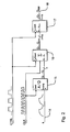
- circuit diagram shown in Figure 2 showed an unclaimed circuit arrangement for averaging, which can be dispensed with a sigma-delta modulator.
- This circuit arrangement has a signal input 14 for receiving an evaluated input signal s, wherein the input signal s may be, for example, a current signal of an electronic transmission control in a passenger car.
- the input signal s is supplied to a sampling input ANALOG IN of an analog-to-digital converter 15, which generates from the input signal s a digital signal Q 1 ... Q n with a width of n bits.
- the analog / digital converter 15 is in this case clocked by a clock signal CLK, which is applied to a clock input CLOCK of the analog / digital converter 15 and determines the sampling rate.
- the clock signal CLK is generated by a microcontroller, which is not shown for simplicity, wherein the clock frequency of the clock signal CLK is much greater than the cut-off frequency of the band-limited input signal s, so that an oversampling is given and no signal information is lost.
- the clock frequency of the clock signal 32 times as large as the cutoff frequency of the input signal s, resulting in a good signal / noise ratio.
- the analog / digital converter 15 is connected to a summer 16, which summed up the input digital signals Q 1 ... Q n and the output side a corresponding digital signal Q 1 ... Q n + m with a word length of n + m bits outputs.
- the summer 16 is also clocked by the clock signal CLK, so that all the digital signals Q 1 ... Q n are summed, which are sampled by the analog / digital converter 15.
- the summer 16 has a reset input RESET, to which a control signal CTRL is supplied, which is generated by the microcontroller, not shown.
- the control signal CTRL is generated by the microcontroller in such a way that there is always a constant phase relationship between the input signal s and the control signal CTRL. In this way it is achieved that in each case the same time window of the periodic input signal s is evaluated, since the summer 16 is reset by the control signal CTRL.
- the sum Q 1 ... Q n + m of all the digital signals Q 1 ... Q n appears during the respective current period.
- the summer 16 On the output side, the summer 16 is connected to an output register 17, which temporarily stores the determined sum during the next period. At the end of the next period, the new summation value is then transferred to the output register 17.
- the acquisition of the new sum value from the summer 16 in the output register 17 is controlled by a control input LATCH, at which the control signal CTRL is present.
- the output register 17 then outputs at a signal output 18 an output signal Q 1 ... Q n + m which represents the sum of the sampled values during the last period. From this, the temporal mean value during the last period can then be calculated in conjunction with the number of samples or the sampling rate.
Landscapes
- Physics & Mathematics (AREA)
- Nonlinear Science (AREA)
- General Physics & Mathematics (AREA)
- Compression, Expansion, Code Conversion, And Decoders (AREA)
Description
- Die Erfindung betrifft eine Schaltungsanordnung zur Mittelwertbildung gemäß dem Oberbegriff des Anspruchs 1.
- Gattungsgemäße Schattungsanordnunggen sind aus den Dokumenten EP-A-0 804 038, US-A-5 329 281 und EP-A-0 367 522 bekannt.
- In der Kraftfahrzeugtechnik werden zur Steuerung eines automatischen Getriebes bekanntermaßen Magnetventile eingesetzt, die mit einem pulsweitenmodulierten Stromsignal angesteuert werden. Hierbei wird der zeitliche Mittelwert des Stroms erfasst, um das Regelverhalten des Magnetventils innerhalb einer Regelstrecke optimieren zu können.
- Hierzu werden bislang herkömmliche analoge Tiefpassfilter verwendet, die Wechselspannungsanteile aus dem Stromsignal weitgehend ausfiltern und den Gleichanteil als Mittelwert ausgeben.
- Nachteilig an der bekannten Mittelwertbildung durch analoge Filter ist zum einen die Einschwingzeit derartiger Filter, so dass der Mittelwert in der Regel erst nach einigen Perioden der Pulsweitenmodulation zur Verfügung steht.
- Zum anderen ist die Mittelwertbildung durch analoge Filter auch relativ ungenau, was ebenfalls unerwünscht ist.
- Der Erfindung liegt also die Aufgabe zugrunde, eine Schaltungsanordnung zu schaffen, die eine möglichst schnelle und genaue Mittelwertbildung ermöglicht.
- Die Aufgabe wird, ausgehend von einer bekannten Schaltungsanordnung gemäß dem Oberbegriff des Anspruchs 1, durch die kennzeichnenden Merkmale des Anspruchs 1 gelöst.
- Die Erfindung umfasst die allgemeine technische Lehre, zwischen dem Signaleingang und dem Signalausgang der Schaltungsanordnung einen Summierer oder einen Zähler für die Mittelwertbildung vorzusehen.
- Vor der eigentlichen Mittelwertbildung wird das auszuwertende Eingangssignal also vorzugsweise zunächst digitalisiert, so dass die Mittelwertbildung ohne die dynamischen Probleme analoger Filter im Digitalbereich erfolgen kann.
- In einer bevorzugten Ausführungsform der Erfindung ist der Summierer bzw. Zähler eingangsseitig mit einem Sigma-Delta-Modulator verbunden, der das auszuwertende Eingangssignal einer Sigma-Delta-Modulation unterzieht und das auf diese Weise modulierte Signal dem Summierer bzw. Zähler zuführt. Derartige Sigma-Delta-Modulatoren sind beispielsweise aus NORSWORTHY/SCHREIER/TEMES: "Delta-Sigma Data Converters" (IEEE Press), aus CANDY/TEMES: "Oversampling Delta-Sigma Data Converters : Theory, Design and Simulation" (IEEE Press) sowie aus ENGELEN/PLASSCHE: "Bandpass Sigma Delta Modulators" (Kluwer Academic Publishers) bekannt.
- Der Sigma-Delta-Modulator sollte hierbei mit einer Taktfrequenz bzw. Abtastrate arbeiten, die größer als die Nyquist-Rate des Eingangssignals ist, damit eine Überabtastung erfolgt und keine Signalinformationen des Eingangssignals verloren gehen.
- Bei einem periodischen Eingangssignal ist es weiterhin vorteilhaft, wenn stets dasselbe Zeitfenster des Eingangssignals ausgewertet wird. Dies ist sinnvollerweise die einfache oder vielfache Periodendauer des Eingangssignals. Der Zähler weist deshalb vorzugsweise einen Rücksetzeingang auf, dem ein Steuersignal zugeführt wird, das beispielsweise von einem Mikrocontroller erzeugt wird. Vorzugsweise stehen das Steuersignal und das auszuwertende Eingangssignal in einer zeitlich konstanten Phasenbeziehung zueinander, damit stets dasselbe Zeitfenster des Eingangssignals ausgewertet wird.
- Bei einem periodischen Eingangssignal ist es weiterhin vorteilhaft, wenn das Eingangssignal und das Taktsignal des Sigma-Delta-Modulators in einer zeitlich konstanten Phasenbeziehung zueinander stehen, damit stets dasselbe Zeitfenster des Eingangssignals ausgewertet wird. Vorzugsweise wird das Eingangssignal für den Sigma-Delta-Modulator deshalb aus dem auszuwertenden Taktsignal abgeleitet, wozu beispielsweise ein herkömmlicher Mikrocontroller verwendet werden kann.
- Weiterhin ist zu erwähnen, dass der Sigma-Delta-Modulator wahlweise analog oder digital ausgeführt sein kann.
- Vorzugsweise weist der Sigma-Delta-Modulator eingangsseitig einen Addierer bzw. einen Subtrahierer, einen Integrator sowie ausgangsseitig einen Komparator auf, wobei der Ausgang des Komparators in einer Rückkopplungsschleife auf einen Eingang des Addierers bzw. Subtrahierers zurückgeführt ist.
- Der Integrator des Sigma-Delta-Modulators kann beispielsweise als Integrator erster Ordnung ausgeführt sein, jedoch können auch Integratoren höherer Ordnung in dem Sigma-Delta-Modulator verwendet werden, wodurch sich vorteilhaft eine höhere Auflösung erreichen lässt.
- Der ausgangsseitig in dem Sigma-Delta-Modulator angeordnete Komparator weist eine vorgegebene Entscheidungsschwelle auf, die vorzugsweise einem Nullpegel des Eingangssignals entspricht. Beim Überschreiten der Entscheidungsschwelle gibt der Komparator vorzugsweise einen positiven Pegel aus, wohingegen der Komparator beim Unterschreiten der Entscheidungsschwelle vorzugsweise einen negativen Pegel ausgibt.
- In einer bevorzugten Ausführungsform der Erfindung wird der Ausgang des Komparators in der Rückkopplungsschleife nicht direkt auf den Eingang des Addierers bzw. Subtrahierers zurückgeführt, sondern zur Ansteuerung eines Schaltelements verwendet, das wahlweise ein erstes Referenzsignal oder ein zweites Referenzsignal auf den Eingang des Addierers bzw. Subtrahierers schaltet. Dies ist vorteilhaft, da das Ausgangssignal des Komparators Ungenauigkeiten aufweisen kann, die auf diese Weise nicht zurückgekoppelt und somit unterdrückt werden. Die Referenzsignale können dagegen durch Referenzsignalquellen mit hoher Genauigkeit und Konstanz erzeugt werden, so dass die Genauigkeit der Mittelwertbildung durch diese indirekte Rückkopplung erhöht wird.
- In einer anderen, nicht beanspruchten Variante ist dagegen kein Sigma-Delta-Modulator erforderlich, wobei eingangsseitig ein Analog/Digital-Wandler vorgesehen ist, der das auszuwertende analoge Eingangssignal abtastet, in ein Digitalsignal umgewandelt und anschließend direkt oder indirekt dem Summierer bzw. dem Zähler zugeführt. Aus der Anzahl der vorangegangenen Abtastungen und dem Ausgangssignal des Summierers bzw. Zählers kann dann in einfacher Weise der zeitliche Mittelwert des Eingangssignals bestimmt werden, indem das Ausgangssignal des Summierers durch die Anzahl der aufaddierten Abtastwerte geteilt wird.
- Der Analog/Digital-Wandler sollte hierbei ebenfalls mit einer Abtastrate arbeiten, die größer als die Nyquist-Rate des Eingangssignals ist, damit eine Überabtastung erfolgt und keine Signalinformationen des Eingangssignals verloren gehen.
- Bei einem bandbegrenzten Eingangssignal mit einer vorgegebenen oberen Grenzfrequenz ist die Taktfrequenz des Analog/Digitalwandlers deshalb vorzugsweise ein ganzzahliges Vielfaches der Grenzfrequenz des auszuwertenden Eingangssignals, wobei eine Überabtastung mit einem Faktor von 16, 32 oder 64 vorteilhaft ist, um einen ausreichenden Signal/Rauschabstand zu erzielen.
- Bei einem periodischen Eingangssignal ist es weiterhin vorteilhaft, wenn stets dasselbe Zeitfenster des Eingangssignals abgetastet wird. Der Summierer weist deshalb vorzugsweise einen Rücksetzeingang auf, dem ein Steuersignal zugeführt wird, das beispielsweise von einem Mikrocontroller erzeugt wird. Vorzugsweise stehen das Steuersignal und das auszuwertende Eingangssignal in einer zeitlich konstanten Phasenbeziehung zueinander, damit stets dasselbe Zeitfenster des Eingangssignals ausgewertet wird.
- In den beiden vorstehend beschriebenen Varianten mit einem Sigma-Delta-Modulator einerseits und mit einem schneller Analog/Digital-Wandler andererseits ist ausgangsseitig vorzugsweise ein Ausgangsregister vorgesehen, dass den Mittelwert zwischenspeichert, bis der nächste Mittelwert berechnet wurde.
- Die erfindungsgemäße Schaltungsanordnung eignet sich vorzugsweise zur Mittelwertbildung bei Strom- und Spannungssignalen in der Kraftfahrzeugtechnik. Beispielsweise kann das auszuwertende Eingangssignal - wie schon eingangs angedeutet wurde - ein Stromsignal sein, mit dem ein Magnetventil angesteuert wird.
- Weiterhin ist zu erwähnen, dass die erfindungsgemäße Schaltungsanordnung nicht notwendigerweise als separate Schaltung ausgeführt sein muss. Es ist vielmehr auch möglich, dass die erfindungsgemäße Schaltungsanordnung Bestandteil einer komplexen elektronischen Schaltung ist, die neben der Mittelwertbildung auch andere Funktionen erfüllt.
- Andere vorteilhafte Weiterbildungen der Erfindung sind in den abhängigen Ansprüchen enthalten oder werden nachstehend zusammen mit der Beschreibung der bevorzugten Ausführungsbeispiele der Erfindung anhand der Zeichnungen erläutert. Es zeigen:
- Figur 1
- ein Schaltbild einer erfindungsgemäßen Schaltungsanordnung mit einem Sigma-Delta-Modulator zur Mittelwertbildung sowie
- Figur 2
- ein Schaltbild einer alternativen Schaltungsanordnung mit einem schnellen Analog/Digital-Wandler anstelle eines Sigma-Delta-Modulators.
- Die in Figur 1 dargestellte Schaltungsanordnung kann beispielsweise in einer elektronischen Getriebesteuerung eines Kraftfahrzeugs eingesetzt werden, um den zeitlichen Mittelwert eines Stromsignals s zu ermitteln.
- Hierzu weist die erfindungsgemäße Schaltungsanordnung einen Signaleingang 1 auf, an dem das auszuwertende Stromsignal s anliegt.
- Dem Signaleingang 1 ist ein Sigma-Delta-Modulator 2 nachgeschaltet, der analog aufgebaut ist und aus einem Addierer 3, einem Integrator 4 und einem Komparator 5 besteht.
- Der Addierer 3 weist einen nicht-invertierenden Eingang auf, der mit dem Signaleingang 1 der erfindungsgemäße Schaltungsanordnung verbunden ist und das Eingangssignal s aufnimmt.
- Weiterhin weist der Addierer 3 einen invertierenden Eingang auf, der über ein Schaltelement 6 wahlweise mit einer von zwei Referenzsignalquellen 7, 8 verbunden werden kann. Die Referenzsignalquelle 7 erzeugt hierbei ein Referenzsignal Neg_Ref mit einer negativen Polarität, wohingegen die Referenzsignalquelle 8 ein Referenzsignal Pos_Ref mit einer positiven Polarität erzeugt.
- Die Ansteuerung des Schaltelements 6 erfolgt in Abhängigkeit von dem Signal, das am Ausgang des Komparators 5 erscheint. Hierzu weist das Schaltelement 6 einen Steuereingang auf, der mit dem Ausgang des Komparators 5 verbunden ist.
- Falls das Ausgangssignal des Komparators 5 eine positive Polarität aufweist, so verbindet das Schaltelement 6 den invertierenden Eingang des Addierers 3 mit der Referenzsignalquelle 8.
- Falls das Ausgangssignal des Komparators 5 dagegen eine negative Polarität aufweist, so verbindet das Schaltelement 6 den invertierenden Eingang des Addierers 3 mit der Referenzsignalquelle 7.
- Diese indirekte Rückkopplung des Komparatorausgangs auf den invertierenden Eingang des Addierers bietet gegenüber einer direkten Rückkopplung den Vorteil, dass die Referenzsignalquellen 7, 8 ein wesentlich genaueres und zeitliches konstanteres Signal erzeugen können, wohingegen das Ausgangssignal des Komparators 5 Ungenauigkeiten aufweist.
- Ausgangsseitig ist der Addierer 3 mit dem Eingang des Integrators 4 verbunden, wobei der Integrator 4 ein Integrator erster Ordnung ist, um eine einfache schaltungstechnische Realisierung zu ermöglichen.
- Der Integrator 4 ist ausgangsseitig wiederum mit dem Komparator 5 verbunden, der das Ausgangssignal des Integrators 4 mit einer Entscheidungsschwelle vergleicht, die einem Null-Pegel des Eingangssignals s entspricht.
- Beim Überschreiten der Entscheidungsschwelle gibt der Komparator 5 ein Ausgangssignal mit einer positiven Polarität aus, so dass der Schalter 6 den invertierenden Eingang des Addierers 3 mit der Referenzsignalquelle 8 verbindet.
- Beim Unterschreiten der Entscheidungsschwelle gibt der Komparator 6 dagegen ein Ausgangssignal mit einer negativen Polarität aus, so dass der Schalter 6 den invertierenden Eingang des Addierers 3 mit der Referenzsignalquelle 7 verbindet.
- Die Ansteuerung des Schalters 6 und eines Zählers 10 durch den Komparator 5 erfolgt hierbei taktgesteuert durch ein Taktsignal CLK, das von einem Mikrocontroller erzeugt wird und an einem Takteingang 9 anliegt. Die Taktfrequenz fCLK des Taktsignals CLK ist hierbei 2n mal so groß wie die Grenzfrequenz fs des bandbegrenzten Eingangssignals s, wobei n ganzzahlig und größer oder gleich 1 ist. Dies ist sinnvoll, damit eine Überabtastung gegeben ist und keine Signalinformationen verloren gehen.
- Ausgangsseitig ist der Sigma-Delta-Modulator 2 mit einem Freigabe-Eingang ENABLE des Zählers 10 verbunden. Ein High-Pegel an dem Freigabe-Eingang ENABLE ermöglicht also einen Zählvorgang, bei dem der Zählerstand in dem Zähler 10 inkrementiert wird.
- Weiterhin weist der Zähler 10 einen Takteingang CLOCK auf, der mit dem Takteingang 9 verbunden ist und somit ebenfalls durch das Taktsignal CLK angesteuert wird.
- Darüber hinaus hat der Zähler einen Rücksetzeingang RESET, der mit einem Steuersignal CTRL beaufschlagt wird, wobei das Steuersignal CTRL an einem Steuereingang 11 anliegt und von einem Mikrocontroller erzeugt. Hierbei ist zu erwähnen, dass das Steuersignal CTRL von dem Mikrocontroller so erzeugt wird, das stets eine konstante Phasenbeziehung zwischen dem Eingangssignal s und dem Steuersignal CTRL besteht. Auf diese Weise wird erreicht, dass jeweils dasselbe Zeitfenster des periodischen Eingangssignals s ausgewertet wird, da der Zähler 10 von dem Steuersignal CTRL zurückgesetzt wird.
- Der Zählerstand des Zählers 10 gibt also den zeitlichen Mittelwert des Eingangssignals s während der laufenden Periode der Pulsweitenmodulation wieder.
- Ausgangsseitig ist der Zähler 10 mit einem Ausgangsregister 12 verbunden, das den Zählerstand während der nächsten Periode zwischenspeichert. Am Ende der nächsten Periode wird dann der neue Zählerstand in das Ausgangsregister übernommen. Die Übernahme des Zählerstands in das Ausgangsregister 12 wird hierbei durch einen Steuereingang LATCH gesteuert, an dem das Steuersignal CTRL anliegt.
- An einem Signalausgang 13 gibt die erfindungsgemäße Schaltungsanordnung schließlich ein Ausgangssignal g aus, das den zeitliche Mittelwert des Eingangssignals s während der letzten Perioden wiedergibt.
- Das in Figur 2 dargestellte Schaltbild zeigte eine nicht beanspruchte Schaltungsanordnung zur Mittelwertbildung, bei der auf einen Sigma-Delta-Modulator verzichtet werden kann.
- Diese Schaltungsanordnung weist zur Aufnahme eines auszuwertenden Eingangssignals s einen Signaleingang 14 auf, wobei es sich bei dem Eingangssignal s beispielsweise um ein Stromsignal einer elektronischen Getriebesteuerung in einem PKW handeln kann.
- Das Eingangssignal s wird einem Abtasteingang ANALOG IN eines Analog/Digital-Wandlers 15 zugeführt, der aus dem Eingangssignal s ein Digitalsignal Q1...Qn mit einer Breite von n Bit erzeugt.
- Der Analog/Digital-Wandler 15 wird hierbei durch ein Taktsignal CLK getaktet, das an einem Takteingang CLOCK des Analog/Digital-Wandlers 15 anliegt und die Abtastrate festlegt.
- Das Taktsignal CLK wird von einem Mikrocontroller erzeugt, der zur Vereinfachung nicht dargestellt ist, wobei die Taktfrequenz des Taktsignals CLK wesentlich größer ist als die Grenzfrequenz des bandbegrenzten Eingangssignals s, damit eine Überabtastung gegeben ist und keine Signalinformationen verloren gehen. In diesem Ausführungsbeispiel ist die Taktfrequenz des Taktsignals 32 mal so groß wie die Grenzfrequenz des Eingangssignals s, woraus sich auch ein guter Signal/Rausch-Abstand ergibt.
- Ausgangsseitig ist der Analog/Digital-Wandler 15 mit einem Summierer 16 verbunden, der die eingangsseitig aufgenommenen Digitalsignale Q1...Qn aufsummiert und ausgangsseitig ein entsprechendes Digitalsignal Q1...Qn+m mit einer Wortlänge von n+m Bit ausgibt.
- Der Summierer 16 wird hierbei ebenfalls von dem Taktsignal CLK getaktet, so dass sämtliche Digitalsignale Q1...Qn aufsummiert werden, die von dem Analog/Digital-Wandler 15 abgetastet werden.
- Weiterhin weist der Summierer 16 einen Rücksetzeingang RESET auf, dem ein Steuersignal CTRL zugeführt wird, das von dem nicht dargestellten Mikrocontroller erzeugt wird. Hierbei ist wiederum zu erwähnen, dass das Steuersignal CTRL von dem Mikrocontroller so erzeugt wird, das stets eine konstante Phasenbeziehung zwischen dem Eingangssignal s und dem Steuersignal CTRL besteht. Auf diese Weise wird erreicht, dass jeweils dasselbe Zeitfenster des periodischen Eingangssignals s ausgewertet wird, da der Summierer 16 von dem Steuersignal CTRL zurückgesetzt wird. Am Ausgang des Summierers 16 erscheint also die Summe Q1...Qn+m sämtlicher Digitalsignale Q1...Qn während der jeweils laufenden Periode.
- Ausgangsseitig ist der Summierer 16 mit einem Ausgangsregister 17 verbunden, das die ermittelte Summe während der nächsten Periode zwischenspeichert. Am Ende der nächsten Periode wird dann der neue Summenwert in das Ausgangsregister 17 übernommen. Die Übernahme des neuen Summenwerts von dem Summierer 16 in das Ausgangsregister 17 wird hierbei durch einen Steuereingang LATCH gesteuert, an dem das Steuersignal CTRL anliegt.
- Ausgangsseitig gibt das Ausgangsregister 17 dann an einem Signalausgang 18 ein Ausgangssignal Q1...Qn+m aus, das die Summe der Abtastwerte während der letzten Periode wiedergibt. Daraus kann dann in Verbindung mit der Anzahl der Abtastungen bzw. der Abtastrate der zeitliche Mittelwert während der letzten Periode berechnet werden.
Claims (8)
- Schaltungsanordnung zur Bestimmung des Mittelwerts eines Eingangssignals (s), mit
einem Signaleingang (1) zur Aufnahme des Eingangssignals (s) und
einem Signalausgang (13) zur Ausgabe eines den Mittelwert des Eingangssignals (s) wiedergebenden Ausgangssignals (g),
wobei zwischen dem Signaleingang (1) und dem Signalausgang (13) zur Mittelwertbildung ein Zähler (10) oder ein Summierer angeordnet ist, der eingangsseitig mit einem Komparator (5) verbunden ist,
wobei in einer Rückkopplungsschleife ein Schaltelement (6) angeordnet ist, das von dem Ausgang des Komparators (5) angesteuert wird und in Abhängigkeit von dem Ausgang des Komparators (5) ein erstes Referenzsignal (Pos_Ref) oder ein zweites Referenzsignal (Neg_Ref) aufschaltet;
dadurch gekennzeichnet,
dass der Summierer oder der Zähler (10) einen Rücksetzeingang (RESET) aufweist, an dem ein Steuersignal (CTRL) anliegt, wobei das Steuersignal (CTRL) und das Eingangssignal (s) die gleiche Grundfrequenz und/oder die gleiche Phasenlage und/oder eine konstante Phasenbeziehungen zueinander aufweisen. - Schaltungsanordnung nach Anspruch 1,
dadurch gekennzeichnet,
dass der Summierer oder der Zähler (10) eingangsseitig mit einem Sigma-Delta-Modulator (2) verbunden ist. - Schaltungsanordnung nach Anspruch 2,
dadurch gekennzeichnet,
dass der Sigma-Delta-Modulator (2) einen Addierer (3) oder einen Subtrahierer, einen Integrator (4) und einen Komparator (5) sowie eine Rückkopplungsschleife von dem Ausgang des Komparators (5) auf den Eingang des Addierers (3) oder Subtrahierers aufweist. - Schaltungsanordnung nach mindestens einem der vorhergehenden Ansprüche,
dadurch gekennzeichnet,
dass der Summierer oder der Zähler (10) einen Takteingang (CLOCK) aufweist, an dem ein Taktsignal (CLK) mit einer vorgegebenen Taktfrequenz anliegt. - Schaltungsanordnung nach Anspruch 4,
dadurch gekennzeichnet,
dass das Eingangssignal (s) bandbegrenzt ist und eine vorgegebene Grenzfrequenz aufweist, wobei die Taktfrequenz ein ganzzahliges Vielfaches der Grenzfrequenz ist. - Schaltungsanordnung nach einem der vorhergehenden Ansprüche,
dadurch gekennzeichnet,
dass das Taktsignal (CLK) und das Steuersignal (CTRL) eine zeitlich konstante Phasenbeziehung zueinander aufweisen. - Schaltungsanordnung nach mindestens einem der vorhergehenden Ansprüche,
dadurch gekennzeichnet,
dass der Summierer oder Addierer oder der Zähler (10) ausgangsseitig mit einem Ausgangsregister (12) verbunden ist. - Schaltungsanordnung nach Anspruch 7,
dadurch gekennzeichnet,
dass das Ausgangsregister (12) einen Steuereingang (LATCH) zur Steuerung der Datenaufnahme aufweist, wobei an dem Steuereingang (LATCH) das Steuersignal (CTRL) anliegt.
Applications Claiming Priority (3)
| Application Number | Priority Date | Filing Date | Title |
|---|---|---|---|
| DE10243564 | 2002-09-19 | ||
| DE10243564A DE10243564B4 (de) | 2002-09-19 | 2002-09-19 | Schaltungsanordnung zur Mittelwertbildung |
| PCT/DE2003/002580 WO2004030211A2 (de) | 2002-09-19 | 2003-07-31 | Schaltungsanordnung zur mittelwertbildung |
Publications (2)
| Publication Number | Publication Date |
|---|---|
| EP1540821A2 EP1540821A2 (de) | 2005-06-15 |
| EP1540821B1 true EP1540821B1 (de) | 2006-02-15 |
Family
ID=31983952
Family Applications (1)
| Application Number | Title | Priority Date | Filing Date |
|---|---|---|---|
| EP03798049A Expired - Lifetime EP1540821B1 (de) | 2002-09-19 | 2003-07-31 | Schaltungsanordnung zur mittelwertbildung |
Country Status (6)
| Country | Link |
|---|---|
| US (1) | US7493355B2 (de) |
| EP (1) | EP1540821B1 (de) |
| JP (1) | JP4041493B2 (de) |
| KR (1) | KR101024418B1 (de) |
| DE (2) | DE10243564B4 (de) |
| WO (1) | WO2004030211A2 (de) |
Families Citing this family (6)
| Publication number | Priority date | Publication date | Assignee | Title |
|---|---|---|---|---|
| BRPI0611954A2 (pt) * | 2005-06-10 | 2009-04-28 | Univ Florida State Res Found | processos para a produÇço de compostos de anel fundido policÍclico |
| DE102008015841A1 (de) | 2008-03-27 | 2009-10-01 | Continental Teves Ag & Co. Ohg | Elektronisches Kraftfahrzeugregelungssystem mit Strommessschaltung |
| RU2444125C2 (ru) * | 2009-08-03 | 2012-02-27 | Государственное Образовательное Учреждение Высшего Профессионального Образования "Омский Государственный Технический Университет" | Способ аналого-цифрового преобразования измерительных сигналов |
| KR101634359B1 (ko) * | 2009-09-23 | 2016-06-28 | 삼성전자주식회사 | 클럭 신호의 변화를 통하여 이득을 제어하는 아날로그-디지털 컨버터 및 이를 포함하는 이미지 센서 |
| JP5297408B2 (ja) * | 2010-03-26 | 2013-09-25 | アイシン・エィ・ダブリュ株式会社 | 電磁弁の制御装置 |
| US11890923B2 (en) | 2020-06-24 | 2024-02-06 | Honda Motor Co., Ltd. | Upper body heat exchanger for vehicles |
Family Cites Families (17)
| Publication number | Priority date | Publication date | Assignee | Title |
|---|---|---|---|---|
| DE2541421C3 (de) * | 1975-09-17 | 1980-07-03 | Fernsteuergeraete Kurt Oelsch Kg, 1000 Berlin | Meßanordnung zur Mittelwertbildung |
| FR2448722A1 (fr) * | 1979-02-09 | 1980-09-05 | Enertec | Procedes et appareils pour l'analyse de formes d'ondes periodiques |
| FR2478320A1 (fr) * | 1980-03-17 | 1981-09-18 | Telediffusion Fse | Dispositif d'acquisition et de moyennage des echantillons d'un signal periodique bruite |
| DE3045033A1 (de) * | 1980-11-26 | 1982-07-08 | Licentia Patent-Verwaltungs-Gmbh, 6000 Frankfurt | Anordnung zur bestimmung der zeitlichen mittelwerte von analogen messwerten |
| JPH0614610B2 (ja) * | 1984-12-17 | 1994-02-23 | 沖電気工業株式会社 | パルス幅制御回路 |
| DE3509762A1 (de) * | 1985-03-19 | 1986-09-25 | Battelle-Institut E.V., 6000 Frankfurt | Schaltungsanordnung zur mittelwertbildung |
| EP0367522A3 (de) * | 1988-11-02 | 1992-08-05 | Hewlett-Packard Company | Impulsbreiten-Analog/Digitalwandler mit geschlossener Schleife |
| DD300460A5 (de) * | 1990-02-12 | 1992-06-11 | Rostock Baurationalisierung | Vorrichtung zur ständigen Mittelwertbildung einer analogen Meßgröße |
| US5142286A (en) | 1990-10-01 | 1992-08-25 | General Electric Company | Read-out photodiodes using sigma-delta oversampled analog-to-digital converters |
| JPH04144423A (ja) * | 1990-10-05 | 1992-05-18 | Jeol Ltd | Adコンバータ |
| DE69329837T2 (de) * | 1992-04-30 | 2001-04-19 | Hewlett Packard Co | Differenztieller integrierender Verstärker mit geschalteten Kapazitäten zur Bildung von Prezisionswiderständen |
| EP0577902B1 (de) * | 1992-07-10 | 1997-12-10 | International Business Machines Corporation | Dezimationsfilter für einen Sigma-Delta-Wandler und A/D-Wandler mit einem solchen Filter |
| CH689071A5 (de) * | 1994-03-24 | 1998-08-31 | Cerberus Ag | Signalauswertungsschaltung fuer einen Bewegungsmelder. |
| DE69729767T2 (de) * | 1996-04-26 | 2005-07-14 | Hamamatsu Photonics K.K., Hamamatsu | Festkörperbildaufnahmegerät |
| DE10042587B4 (de) * | 2000-08-30 | 2007-04-12 | Infineon Technologies Ag | Filteranordnung und Verfahren zur Filterung eines Analogsignals |
| DE10052152C1 (de) * | 2000-08-31 | 2001-09-06 | Fraunhofer Ges Forschung | Verfahren und Vorrichtung zum Umwandeln eines analogen Eingangssignals in eine Sequenz von digitalen Ausgangswerten |
| US6593870B2 (en) * | 2001-10-18 | 2003-07-15 | Rockwell Automation Technologies, Inc. | MEMS-based electrically isolated analog-to-digital converter |
-
2002
- 2002-09-19 DE DE10243564A patent/DE10243564B4/de not_active Expired - Lifetime
-
2003
- 2003-07-31 EP EP03798049A patent/EP1540821B1/de not_active Expired - Lifetime
- 2003-07-31 WO PCT/DE2003/002580 patent/WO2004030211A2/de not_active Ceased
- 2003-07-31 KR KR1020057004450A patent/KR101024418B1/ko not_active Expired - Lifetime
- 2003-07-31 DE DE50302445T patent/DE50302445D1/de not_active Expired - Lifetime
- 2003-07-31 US US10/528,588 patent/US7493355B2/en not_active Expired - Fee Related
- 2003-07-31 JP JP2004538687A patent/JP4041493B2/ja not_active Expired - Lifetime
Also Published As
| Publication number | Publication date |
|---|---|
| WO2004030211A2 (de) | 2004-04-08 |
| US20060004898A1 (en) | 2006-01-05 |
| JP4041493B2 (ja) | 2008-01-30 |
| KR20050043966A (ko) | 2005-05-11 |
| JP2005538658A (ja) | 2005-12-15 |
| EP1540821A2 (de) | 2005-06-15 |
| DE50302445D1 (de) | 2006-04-20 |
| DE10243564B4 (de) | 2006-11-30 |
| US7493355B2 (en) | 2009-02-17 |
| DE10243564A1 (de) | 2004-04-08 |
| KR101024418B1 (ko) | 2011-03-23 |
| WO2004030211A3 (de) | 2004-07-29 |
Similar Documents
| Publication | Publication Date | Title |
|---|---|---|
| DE69417978T2 (de) | Analog Digitalwandler mit Zittersignal | |
| DE69809870T2 (de) | Delta-Sigma Pulsbreitenmodulator | |
| DE68915700T2 (de) | Verfahren zur Kaskadierung von mehreren Sigma-Delta-Modulatoren und ein Sigma-Delta-Modulatorsystem. | |
| EP0457749B1 (de) | Hochgenauer Analog-Digital-Umsetzer nach dem Ladungsausgleichverfahren | |
| DE69116324T2 (de) | A/D(Analog/Digital)-Wandler | |
| DE3883081T2 (de) | Analog-Digitalumsetzer mit Delta-Sigmamodulation. | |
| DE69620285T2 (de) | Delta-Sigma-Analog-Digitalwandler | |
| DE112012000529T5 (de) | Direkte Rückkopplung für zeitkontinuierliche überabgetastete Wandler | |
| DE112018006099T5 (de) | Techniken zur leistungsreduzierung und leistungsfähigkeitsverbesserung für einen delta-sigma-modulator | |
| EP1001538A2 (de) | Sigma-Delta-Modulator und Verfahren zur Unterdrückung eines Quantisierungsfehlers in einem Sigma-Delta-Modulator | |
| DE102005042710A1 (de) | Vorrichtung und Verfahren zur spektralen Formung eines Referenztaktsignals | |
| DE69223508T2 (de) | Dezimationsfilter für einen Sigma-Delta-Wandler und A/D-Wandler mit einem solchen Filter | |
| DE102018119390B4 (de) | Techniken zur Verringerung von Jitter bei Verwendung digitaler PLL mit ADC und DAC | |
| DE19521610B4 (de) | Dezimationsfilter unter Verwendung einer Nullfüllschaltung zur Lieferung eines wählbaren Dezimationsverhältnisses sowie Verfahren zur Dezimationsfilterung | |
| DE10243564B4 (de) | Schaltungsanordnung zur Mittelwertbildung | |
| DE102006023697B4 (de) | Verfahren zum Decodieren, Decodierer, Codierer-Decodierer-System und Wandler | |
| DE19510655B4 (de) | Schaltungsanordnung zum Filtern eines Stroms quantisierter elektrischer Signale und Verfahren zum Filtern eines Stoms quantisierter elektrischer Signale | |
| DE102004031153B4 (de) | Hochauflösender Sigma-Delta-Wandler | |
| DE10233391C1 (de) | Analog/Digital-Wandlerschaltung sowie entsprechendes Verfahren zur Analog/Digital-Wandlung und Verwendung einer selbstoszillierenden Schaltung zur Analog/Digital-Wandlung | |
| WO1995026079A1 (de) | Schaltungsanordnung zur aufbereitung und a/d-wandlung eines analogen signals | |
| EP1048112B1 (de) | Sigma-delta-d/a-wandler | |
| DE19714142C1 (de) | Phasendetektor | |
| EP2471181A1 (de) | Verfahren zur verarbeitung eines einen analog bestimmten wert für ausgangsstrom eines umrichters darstellenden messwertsignals und vorrichtung zur durchführung des verfahrens | |
| DE102005015390B4 (de) | Quantisierer in einem Multilevel-Sigma-Delta-Analog-Digital-Umsetzer | |
| DE102006054776B4 (de) | Vorrichtung und Verfahren für die Sigma-Delta-Modulation |
Legal Events
| Date | Code | Title | Description |
|---|---|---|---|
| PUAI | Public reference made under article 153(3) epc to a published international application that has entered the european phase |
Free format text: ORIGINAL CODE: 0009012 |
|
| 17P | Request for examination filed |
Effective date: 20050126 |
|
| AK | Designated contracting states |
Kind code of ref document: A2 Designated state(s): AT BE BG CH CY CZ DE DK EE ES FI FR GB GR HU IE IT LI LU MC NL PT RO SE SI SK TR |
|
| GRAP | Despatch of communication of intention to grant a patent |
Free format text: ORIGINAL CODE: EPIDOSNIGR1 |
|
| RBV | Designated contracting states (corrected) |
Designated state(s): DE FR GB IT |
|
| GRAS | Grant fee paid |
Free format text: ORIGINAL CODE: EPIDOSNIGR3 |
|
| GRAA | (expected) grant |
Free format text: ORIGINAL CODE: 0009210 |
|
| AK | Designated contracting states |
Kind code of ref document: B1 Designated state(s): DE FR GB IT |
|
| REG | Reference to a national code |
Ref country code: GB Ref legal event code: FG4D Free format text: NOT ENGLISH |
|
| GBT | Gb: translation of ep patent filed (gb section 77(6)(a)/1977) |
Effective date: 20060227 |
|
| REF | Corresponds to: |
Ref document number: 50302445 Country of ref document: DE Date of ref document: 20060420 Kind code of ref document: P |
|
| ET | Fr: translation filed | ||
| PLBE | No opposition filed within time limit |
Free format text: ORIGINAL CODE: 0009261 |
|
| STAA | Information on the status of an ep patent application or granted ep patent |
Free format text: STATUS: NO OPPOSITION FILED WITHIN TIME LIMIT |
|
| 26N | No opposition filed |
Effective date: 20061116 |
|
| PGFP | Annual fee paid to national office [announced via postgrant information from national office to epo] |
Ref country code: IT Payment date: 20100723 Year of fee payment: 8 |
|
| PGFP | Annual fee paid to national office [announced via postgrant information from national office to epo] |
Ref country code: GB Payment date: 20100722 Year of fee payment: 8 |
|
| REG | Reference to a national code |
Ref country code: FR Ref legal event code: TP |
|
| REG | Reference to a national code |
Ref country code: GB Ref legal event code: 732E Free format text: REGISTERED BETWEEN 20110825 AND 20110831 |
|
| GBPC | Gb: european patent ceased through non-payment of renewal fee |
Effective date: 20110731 |
|
| PG25 | Lapsed in a contracting state [announced via postgrant information from national office to epo] |
Ref country code: IT Free format text: LAPSE BECAUSE OF NON-PAYMENT OF DUE FEES Effective date: 20110731 |
|
| PG25 | Lapsed in a contracting state [announced via postgrant information from national office to epo] |
Ref country code: GB Free format text: LAPSE BECAUSE OF NON-PAYMENT OF DUE FEES Effective date: 20110731 |
|
| REG | Reference to a national code |
Ref country code: FR Ref legal event code: PLFP Year of fee payment: 14 |
|
| REG | Reference to a national code |
Ref country code: FR Ref legal event code: PLFP Year of fee payment: 15 |
|
| REG | Reference to a national code |
Ref country code: FR Ref legal event code: PLFP Year of fee payment: 16 |
|
| PGFP | Annual fee paid to national office [announced via postgrant information from national office to epo] |
Ref country code: FR Payment date: 20190719 Year of fee payment: 17 Ref country code: DE Payment date: 20190731 Year of fee payment: 17 |
|
| REG | Reference to a national code |
Ref country code: DE Ref legal event code: R084 Ref document number: 50302445 Country of ref document: DE |
|
| REG | Reference to a national code |
Ref country code: DE Ref legal event code: R081 Ref document number: 50302445 Country of ref document: DE Owner name: VITESCO TECHNOLOGIES GMBH, DE Free format text: FORMER OWNER: CONTINENTAL AUTOMOTIVE GMBH, 30165 HANNOVER, DE |
|
| REG | Reference to a national code |
Ref country code: DE Ref legal event code: R119 Ref document number: 50302445 Country of ref document: DE |
|
| PG25 | Lapsed in a contracting state [announced via postgrant information from national office to epo] |
Ref country code: FR Free format text: LAPSE BECAUSE OF NON-PAYMENT OF DUE FEES Effective date: 20200731 |
|
| PG25 | Lapsed in a contracting state [announced via postgrant information from national office to epo] |
Ref country code: DE Free format text: LAPSE BECAUSE OF NON-PAYMENT OF DUE FEES Effective date: 20210202 |
|
| REG | Reference to a national code |
Ref country code: DE Ref legal event code: R081 Ref document number: 50302445 Country of ref document: DE Owner name: VITESCO TECHNOLOGIES GMBH, DE Free format text: FORMER OWNER: VITESCO TECHNOLOGIES GMBH, 30165 HANNOVER, DE |