EP1533848A2 - Elktrolumineszente Anzeigevorrichtung - Google Patents
Elktrolumineszente Anzeigevorrichtung Download PDFInfo
- Publication number
- EP1533848A2 EP1533848A2 EP04090447A EP04090447A EP1533848A2 EP 1533848 A2 EP1533848 A2 EP 1533848A2 EP 04090447 A EP04090447 A EP 04090447A EP 04090447 A EP04090447 A EP 04090447A EP 1533848 A2 EP1533848 A2 EP 1533848A2
- Authority
- EP
- European Patent Office
- Prior art keywords
- power supply
- supply voltage
- line
- electro luminescence
- luminescence display
- Prior art date
- Legal status (The legal status is an assumption and is not a legal conclusion. Google has not performed a legal analysis and makes no representation as to the accuracy of the status listed.)
- Granted
Links
Images


Classifications
-
- H—ELECTRICITY
- H10—SEMICONDUCTOR DEVICES; ELECTRIC SOLID-STATE DEVICES NOT OTHERWISE PROVIDED FOR
- H10K—ORGANIC ELECTRIC SOLID-STATE DEVICES
- H10K59/00—Integrated devices, or assemblies of multiple devices, comprising at least one organic light-emitting element covered by group H10K50/00
- H10K59/10—OLED displays
- H10K59/12—Active-matrix OLED [AMOLED] displays
- H10K59/131—Interconnections, e.g. wiring lines or terminals
-
- G—PHYSICS
- G09—EDUCATION; CRYPTOGRAPHY; DISPLAY; ADVERTISING; SEALS
- G09G—ARRANGEMENTS OR CIRCUITS FOR CONTROL OF INDICATING DEVICES USING STATIC MEANS TO PRESENT VARIABLE INFORMATION
- G09G3/00—Control arrangements or circuits, of interest only in connection with visual indicators other than cathode-ray tubes
- G09G3/20—Control arrangements or circuits, of interest only in connection with visual indicators other than cathode-ray tubes for presentation of an assembly of a number of characters, e.g. a page, by composing the assembly by combination of individual elements arranged in a matrix no fixed position being assigned to or needed to be assigned to the individual characters or partial characters
-
- H—ELECTRICITY
- H10—SEMICONDUCTOR DEVICES; ELECTRIC SOLID-STATE DEVICES NOT OTHERWISE PROVIDED FOR
- H10D—INORGANIC ELECTRIC SEMICONDUCTOR DEVICES
- H10D89/00—Aspects of integrated devices not covered by groups H10D84/00 - H10D88/00
- H10D89/10—Integrated device layouts
Definitions
- the present invention relates to an electro luminescence display and, more particularly, to an electro luminescence display in which an electromagnetic interference (EMI) shielding means capable of shielding the EMI by having a shielding means in a first power supply voltage line is contained to prevent noise or the like of the power supply voltage due to an internal or external EMI from occurring.
- EMI electromagnetic interference
- Such a flat panel display includes a liquid crystal display, a field emission display, a plasma display panel, an electro luminescence display, and the like.
- the electro luminescence display uses carriers such as electrons and holes to excite a fluorescent material to display image or video so that it may be driven by a low direct voltage and has a faster response speed.
- the electro luminescence display has been in the spotlight as the next generation display and researches on new products have accelerated in recent years.
- This electro luminescence display may be mainly classified into a passive matrix type and an active matrix type, and the active matrix electro luminescence display has an active switching device arranged in each pixel and has a voltage or current in response to the image data of the pixel applied to drive each emitting device.
- Such an active matrix type electro luminescence display is shown in FIG. 1.
- FIG. 1 is a plan view of a conventional active matrix type electro luminescence display.
- Numerical reference 100 indicates an electro luminescence display
- 110 indicates a first upper power supply voltage line
- 120 indicates a first lower power supply voltage line
- 130 indicates a second power supply voltage line
- 140 indicates a scan driver
- 150 indicates a data driver
- 160 indicates a first active power supply voltage line
- 170 indicates a pixel region.
- the conventional electro luminescence display 100 includes the scan driver 140 applying a selection signal, the data driver 150 applying a data signal, the pixel region 170 emitting light in response to the selection signal and the data signal applied from the scan driver 140 and the data driver 150, the first upper and lower power supply voltage lines 110 and 120 delivering first power supply voltages, the second power supply line 130 delivering a second power supply voltage, and the first active power supply voltage line 160 applying, the power supply voltages delivered from the first power supply voltage lines 110 and 120 and the second power supply voltage delivered to the second power supply voltage line 130, to the pixel region 170.
- each of the first power supply voltages is opposite to that of the second power supply voltage.
- the conventional electro luminescence display as described above has a problem that the waveform of the power supply voltage is distorted due to an internally or externally applied electromagnetic wave. That is, the power supply voltages delivered through the first upper and lower power supply voltage lines have noises which are resulted from the electromagnetic wave externally or internally delivered to thereby have non-uniformity in brightness.
- the present invention therefore, solves aforementioned problems associated with conventional devices by providing an electro luminescence display having an EMI shielding means parallel to first power supply voltage lines wherein a specific voltage is applied to the EMI shielding means to pull the electromagnetic wave so that the electromagnetic wave otherwise affecting the power supply voltage may be shielded.
- an electro luminescence display including: a pixel region in which devices are arranged in a stripe line structure or in a delta line structure to emit light in response to a data signal; a scan driver applying a switching signal to a gate electrode of a first switching device; a data driver applying data information to a source electrode of the first switching device; and a power supply line having a conductive characteristic of applying a first power supply voltage to the pixel region
- the electro luminescence display includes a means for shielding an electromagnetic wave having electronic field or magnetic field characteristics.
- the electro luminescence display may further include a shielding voltage generating means for applying a voltage to the means for shielding the electronic field or magnetic field.
- the means for shielding the electronic field or magnetic field may generate a second power supply voltage.
- the second power supply voltage may have a polarity opposite to that of the first power supply voltage.
- the means for shielding the electronic field or magnetic field may be a conductive interconnection line arranged parallel to the first power supply voltage line.
- an electro luminescence display including: a pixel region in which devices are arranged in a stripe line structure or in a delta line structure to emit light in response to a data signal; a scan driver applying a switching signal to a gate electrode of a first switching device; a data driver applying data information to a source electrode of the first switching device; and a power supply line having a conductive characteristic of applying a first power supply voltage to the pixel region, the electro luminescence display includes a metal line arranged parallel to the first power supply voltage line.
- the metal line may be arranged inside the first power supply voltage line.
- the metal line may be arranged outside the first power supply voltage line.
- the metal lines may be arranged inside and outside the power supply voltage line, respectively.
- the electro luminescence display may further include a shielding voltage generating means for applying a voltage to the metal line.
- the shielding voltage generating means may apply a second power supply voltage having a polarity opposite to that of the first power supply voltage to the metal line.
- an electro luminescence display including: a pixel region in which devices are arranged in a row or in a delta line structure to emit light in response to a data signal; a scan driver applying a switching signal to a gate electrode of a first switching device; a data driver applying data information to a source electrode of the first switching device; and a power supply line having a conductive characteristic of applying a first power supply voltage to the pixel region, the electro luminescence display includes a metal line arranged parallel to the first power supply voltage line to be connected to a ground terminal.
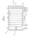
- FIG. 2 is a plan view of a first embodiment of the present invention.
- Numerical reference 200 indicates an electro luminescence display
- 210 indicates a first upper power supply line
- 220 indicates a first lower power supply voltage line
- 230 indicates a second power supply voltage line
- 240 indicates a scan driver
- 250 indicates a data driver
- 260 indicates a first active power supply voltage line
- 270 indicates a pixel region
- 280 indicates a metal line
- 290 indicates a shielding voltage generation means.
- the electro luminescence display 200 includes the scan driver 240, the data driver 250, the pixel region 270 emitting light in response to a selection signal and a data signal applied from the scan driver 240 and the data driver 250, the first upper and lower power supply voltage lines 210 and 220 delivering first power supply voltages, the first active power supply voltage line 260 applying the power supply voltages delivered from the first power supply voltage lines 210 and 220 to the pixel region 270, the second power supply voltage line 230 applying a second power supply voltage to the pixel region 270, the metal line 280 arranged parallel to the first power supply voltage lines 210 and 220 to shield an electromagnetic wave, and the shielding voltage generation means 290 for applying a shielding voltage to the metal line 280.
- switching and drive transistors (not shown) of the pixel region 270 are turned on.
- the drive transistor of the pixel region 270 is turned on, the power supply voltages applied to the first upper and lower power supply voltage lines 210 and 220 are applied to the pixel region 270 through the first active power supply voltage line 260, so that the pixel region 270 emits light.
- the shielding voltage generation means 290 applies a specific voltage to the metal line 280 so that the specific current flows through the metal line 280 arranged parallel to each of the first upper and lower power supply voltage lines 210 and 220.
- the specific voltage applied to the metal line 280 preferably has a polarity opposite to that of each first power supply voltage.
- the metal line 280 and the first power supply voltage line 210 are spaced apart from each other by a constant interval to be parallel to each other as shown in FIGs. 2 and 3, however, the metal line 280 and the first power supply voltage line 210 may be isolated from each other by a separate insulating means interposed therebetween to achieve the purpose of the present invention in cases.
- the electromagnetic wave having magnetic field or electric field characteristics applied from an external source is applied to the first power supply voltage lines 210 and 220
- the electromagnetic wave is shielded by the metal line 280 arranged parallel to the first power supply voltage lines 210 and 220. That is, the voltage applied to the metal line 280 has a polarity opposite to that of the first power supply voltage so that the electromagnetic wave is pulled by the metal line 280 by means of electrical characteristics which flow from positive to negative or from negative to positive.
- the power supply voltage is not affected by the electromagnetic wave.
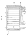
- FIG. 3 is a plan view of a second embodiment of the present invention.
- another embodiment of the present invention has ground terminals 291 each connected to the metal line 280. Accordingly, the electromagnetic wave applied to the first power supply voltage lines 210 and 220 is pulled by the metal line 280 to be grounded so that the power supply voltages are shielded from the electromagnetic wave.
- FIG. 4 is a plan view of a third embodiment of the present invention.
- the metal line 280 is arranged in the first upper power supply voltage line 210 in the first embodiment, however, it may be arranged outside the first upper power supply voltage line 210 in the third embodiment, which also describes the main point of the present invention.
- the metal line 280 is arranged outside the first upper power supply voltage line 210 so as to be spaced apart or insulated from the first upper power supply voltage line 210 by a constant interval or by an insulating means (not shown) respectively, so that the electromagnetic wave applied from an external source may be shielded.
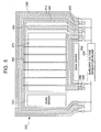
- FIG. 5 is a plan view of a fourth embodiment of the present invention.
- the metal lines 280 are arranged inside and outside the first upper power supply voltage line 210 to shield the electromagnetic wave applied from an external source. That is, a specific voltage is applied to the metal lines 280 arranged inside and outside the first upper power supply voltage line 210 so that the electromagnetic wave applied from the external source may be shielded.
- the electromagnetic wave may be shielded by the metal line arranged parallel to the first power supply voltage lines so that noises of the power supply voltage do not occur, which allows non-uniformity in brightness due to the electromagnetic wave to be improved.
Landscapes
- Engineering & Computer Science (AREA)
- Microelectronics & Electronic Packaging (AREA)
- Physics & Mathematics (AREA)
- Computer Hardware Design (AREA)
- General Physics & Mathematics (AREA)
- Theoretical Computer Science (AREA)
- Control Of Indicators Other Than Cathode Ray Tubes (AREA)
- Electroluminescent Light Sources (AREA)
- Shielding Devices Or Components To Electric Or Magnetic Fields (AREA)
- Devices For Indicating Variable Information By Combining Individual Elements (AREA)
- Control Of El Displays (AREA)
Applications Claiming Priority (2)
| Application Number | Priority Date | Filing Date | Title |
|---|---|---|---|
| KR1020030082391A KR100600865B1 (ko) | 2003-11-19 | 2003-11-19 | 전자파차폐수단을 포함하는 능동소자표시장치 |
| KR2003082391 | 2003-11-19 |
Publications (3)
| Publication Number | Publication Date |
|---|---|
| EP1533848A2 true EP1533848A2 (de) | 2005-05-25 |
| EP1533848A3 EP1533848A3 (de) | 2005-10-19 |
| EP1533848B1 EP1533848B1 (de) | 2014-06-04 |
Family
ID=34431797
Family Applications (1)
| Application Number | Title | Priority Date | Filing Date |
|---|---|---|---|
| EP04090447.6A Expired - Lifetime EP1533848B1 (de) | 2003-11-19 | 2004-11-18 | Elktrolumineszente Anzeigevorrichtung |
Country Status (5)
| Country | Link |
|---|---|
| US (1) | US7372438B2 (de) |
| EP (1) | EP1533848B1 (de) |
| JP (1) | JP2005148757A (de) |
| KR (1) | KR100600865B1 (de) |
| CN (1) | CN1652649A (de) |
Cited By (3)
| Publication number | Priority date | Publication date | Assignee | Title |
|---|---|---|---|---|
| EP1898389A1 (de) * | 2006-09-11 | 2008-03-12 | Samsung SDI Co., Ltd. | Flachbildschirmanzeigevorrichtung |
| CN100452157C (zh) * | 2005-04-26 | 2009-01-14 | 乐金显示有限公司 | 电致发光显示装置 |
| EP4024464A4 (de) * | 2019-08-27 | 2022-09-14 | BOE Technology Group Co., Ltd. | Anzeigesubstrat mit organischen leuchtdioden und herstellungsverfahren dafür sowie anzeigevorrichtung |
Families Citing this family (20)
| Publication number | Priority date | Publication date | Assignee | Title |
|---|---|---|---|---|
| KR100839754B1 (ko) * | 2007-08-14 | 2008-06-19 | 삼성에스디아이 주식회사 | 유기 전계 발광 표시 장치 및 이의 제조 방법 |
| KR101432826B1 (ko) * | 2008-04-29 | 2014-08-27 | 엘지디스플레이 주식회사 | 액정표시장치 및 그 제조방법 |
| TWI424222B (zh) * | 2008-08-28 | 2014-01-21 | Chunghwa Picture Tubes Ltd | 顯示面板 |
| JP5258517B2 (ja) * | 2008-11-10 | 2013-08-07 | 株式会社ジャパンディスプレイウェスト | 電気光学装置及びこれを備えた電子機器 |
| KR101074816B1 (ko) | 2010-05-03 | 2011-10-19 | 삼성모바일디스플레이주식회사 | 표시 장치 |
| KR101701245B1 (ko) * | 2010-10-22 | 2017-02-02 | 삼성디스플레이 주식회사 | 표시 장치 |
| US9029880B2 (en) | 2012-12-10 | 2015-05-12 | LuxVue Technology Corporation | Active matrix display panel with ground tie lines |
| US9159700B2 (en) | 2012-12-10 | 2015-10-13 | LuxVue Technology Corporation | Active matrix emissive micro LED display |
| US9178123B2 (en) | 2012-12-10 | 2015-11-03 | LuxVue Technology Corporation | Light emitting device reflective bank structure |
| US9252375B2 (en) | 2013-03-15 | 2016-02-02 | LuxVue Technology Corporation | Method of fabricating a light emitting diode display with integrated defect detection test |
| US8791474B1 (en) | 2013-03-15 | 2014-07-29 | LuxVue Technology Corporation | Light emitting diode display with redundancy scheme |
| ES2952036T3 (es) | 2013-06-12 | 2023-10-26 | Rohinni Inc | Teclado de retroiluminación con fuentes generadoras de luz depositadas |
| US9111464B2 (en) | 2013-06-18 | 2015-08-18 | LuxVue Technology Corporation | LED display with wavelength conversion layer |
| KR102298484B1 (ko) | 2016-01-15 | 2021-09-03 | 로히니, 엘엘씨. | 장치 상의 커버를 통해 후면 발광하는 장치 및 방법 |
| KR102447435B1 (ko) * | 2016-03-11 | 2022-09-23 | 삼성전자주식회사 | Emi 감소를 위한 전력 전송 네트워크를 포함하는 기판과 이를 포함하는 장치들 |
| CN106601782B (zh) * | 2017-02-22 | 2020-02-28 | 武汉华星光电技术有限公司 | 一种阵列基板及amoled显示装置 |
| KR102377416B1 (ko) * | 2017-06-30 | 2022-03-21 | 엘지디스플레이 주식회사 | 표시장치 |
| US10339869B1 (en) | 2018-02-01 | 2019-07-02 | Wuhan China Star Optoelectronics Semiconductor Display Technology Co., Ltd. | OLED display device |
| CN108364982B (zh) * | 2018-02-01 | 2020-12-22 | 武汉华星光电半导体显示技术有限公司 | Oled显示装置 |
| WO2023225813A1 (zh) * | 2022-05-23 | 2023-11-30 | 京东方科技集团股份有限公司 | 布线基板及电子装置 |
Citations (5)
| Publication number | Priority date | Publication date | Assignee | Title |
|---|---|---|---|---|
| JPS62252964A (ja) | 1986-04-25 | 1987-11-04 | Seiko Epson Corp | ドライバ−内蔵アクティブマトリックス基板 |
| JP2001100233A (ja) | 1999-09-27 | 2001-04-13 | Sharp Corp | 液晶表示装置 |
| US20010022572A1 (en) | 1997-10-31 | 2001-09-20 | Seiko Epson Corporation | Electro-optical apparatus and electronic device |
| US20010055085A1 (en) | 1997-09-26 | 2001-12-27 | Yushi Jinno | Display apparatus and method for manufacturing the same |
| JP2002049330A (ja) | 2000-07-31 | 2002-02-15 | Seiko Epson Corp | 電気光学装置及びそれを有する電子機器並びに投射型表示装置 |
Family Cites Families (25)
| Publication number | Priority date | Publication date | Assignee | Title |
|---|---|---|---|---|
| US5256960A (en) * | 1991-04-09 | 1993-10-26 | Novini Amir R | Portable dual band electromagnetic field radiation measurement apparatus |
| US6771249B1 (en) * | 1995-01-13 | 2004-08-03 | Micron Technology, Inc. | Producing walking one pattern in shift register |
| JP3035188B2 (ja) * | 1995-05-10 | 2000-04-17 | 日本ファウンドリー株式会社 | 半導体装置 |
| JP2778576B2 (ja) | 1996-04-02 | 1998-07-23 | 日本電気株式会社 | Emi対策回路 |
| JP3589005B2 (ja) | 1998-01-09 | 2004-11-17 | セイコーエプソン株式会社 | 電気光学装置及び電子機器 |
| JPH11251779A (ja) | 1998-03-02 | 1999-09-17 | Toshiba Corp | 半導体装置 |
| JP2000048952A (ja) | 1998-07-30 | 2000-02-18 | Tdk Corp | 有機el素子モジュール |
| JP2000086992A (ja) | 1998-09-09 | 2000-03-28 | Unitika Chem Co Ltd | セラミックス用バインダー |
| US7379039B2 (en) * | 1999-07-14 | 2008-05-27 | Sony Corporation | Current drive circuit and display device using same pixel circuit, and drive method |
| JP2001109395A (ja) | 1999-10-01 | 2001-04-20 | Sanyo Electric Co Ltd | El表示装置 |
| JP2001147659A (ja) * | 1999-11-18 | 2001-05-29 | Sony Corp | 表示装置 |
| JP3734664B2 (ja) * | 2000-02-24 | 2006-01-11 | 株式会社日立製作所 | 表示デバイス |
| TW546480B (en) * | 2000-03-07 | 2003-08-11 | Sumitomo Metal Ind | Circuit, apparatus and method for inspecting impedance |
| JP4593740B2 (ja) | 2000-07-28 | 2010-12-08 | ルネサスエレクトロニクス株式会社 | 表示装置 |
| JP2002134744A (ja) * | 2000-10-25 | 2002-05-10 | Nec Corp | 横型絶縁ゲート型電界効果トランジスタ及びその駆動方法 |
| US7015882B2 (en) * | 2000-11-07 | 2006-03-21 | Sony Corporation | Active matrix display and active matrix organic electroluminescence display |
| JP4982014B2 (ja) * | 2001-06-21 | 2012-07-25 | 株式会社日立製作所 | 画像表示装置 |
| KR100470207B1 (ko) * | 2001-08-13 | 2005-02-04 | 엘지전자 주식회사 | 평면 전계방출 표시소자의 구동장치 및 방법 |
| TW563088B (en) * | 2001-09-17 | 2003-11-21 | Semiconductor Energy Lab | Light emitting device, method of driving a light emitting device, and electronic equipment |
| US6762738B2 (en) * | 2001-09-28 | 2004-07-13 | Brillian Corporation | Pixel circuit with shared active regions |
| US7019719B2 (en) * | 2001-10-19 | 2006-03-28 | Clare Micronix Integrated Systems, Inc. | Method and clamping apparatus for securing a minimum reference voltage in a video display boost regulator |
| US7038377B2 (en) | 2002-01-16 | 2006-05-02 | Seiko Epson Corporation | Display device with a narrow frame |
| JP2003271075A (ja) | 2002-03-13 | 2003-09-25 | Toshiba Corp | 表示装置 |
| WO2003092165A1 (fr) * | 2002-04-26 | 2003-11-06 | Toshiba Matsushita Display Technology Co., Ltd. | Circuits a semi-conducteur destines a commander par courant un affichage et affichage correspondant |
| JP4119198B2 (ja) * | 2002-08-09 | 2008-07-16 | 株式会社日立製作所 | 画像表示装置および画像表示モジュール |
-
2003
- 2003-11-19 KR KR1020030082391A patent/KR100600865B1/ko not_active Expired - Lifetime
-
2004
- 2004-11-18 EP EP04090447.6A patent/EP1533848B1/de not_active Expired - Lifetime
- 2004-11-18 JP JP2004335159A patent/JP2005148757A/ja active Pending
- 2004-11-19 CN CNA2004100755968A patent/CN1652649A/zh active Pending
- 2004-11-19 US US10/992,358 patent/US7372438B2/en active Active
Patent Citations (5)
| Publication number | Priority date | Publication date | Assignee | Title |
|---|---|---|---|---|
| JPS62252964A (ja) | 1986-04-25 | 1987-11-04 | Seiko Epson Corp | ドライバ−内蔵アクティブマトリックス基板 |
| US20010055085A1 (en) | 1997-09-26 | 2001-12-27 | Yushi Jinno | Display apparatus and method for manufacturing the same |
| US20010022572A1 (en) | 1997-10-31 | 2001-09-20 | Seiko Epson Corporation | Electro-optical apparatus and electronic device |
| JP2001100233A (ja) | 1999-09-27 | 2001-04-13 | Sharp Corp | 液晶表示装置 |
| JP2002049330A (ja) | 2000-07-31 | 2002-02-15 | Seiko Epson Corp | 電気光学装置及びそれを有する電子機器並びに投射型表示装置 |
Cited By (4)
| Publication number | Priority date | Publication date | Assignee | Title |
|---|---|---|---|---|
| CN100452157C (zh) * | 2005-04-26 | 2009-01-14 | 乐金显示有限公司 | 电致发光显示装置 |
| EP1898389A1 (de) * | 2006-09-11 | 2008-03-12 | Samsung SDI Co., Ltd. | Flachbildschirmanzeigevorrichtung |
| EP4024464A4 (de) * | 2019-08-27 | 2022-09-14 | BOE Technology Group Co., Ltd. | Anzeigesubstrat mit organischen leuchtdioden und herstellungsverfahren dafür sowie anzeigevorrichtung |
| US11737303B2 (en) | 2019-08-27 | 2023-08-22 | Boe Technology Group Co., Ltd. | Organic light-emitting diode display substrate and manufacturing method thereof, display device |
Also Published As
| Publication number | Publication date |
|---|---|
| US20050104530A1 (en) | 2005-05-19 |
| EP1533848B1 (de) | 2014-06-04 |
| KR100600865B1 (ko) | 2006-07-14 |
| EP1533848A3 (de) | 2005-10-19 |
| US7372438B2 (en) | 2008-05-13 |
| CN1652649A (zh) | 2005-08-10 |
| JP2005148757A (ja) | 2005-06-09 |
| KR20050048711A (ko) | 2005-05-25 |
Similar Documents
| Publication | Publication Date | Title |
|---|---|---|
| EP1533848A2 (de) | Elktrolumineszente Anzeigevorrichtung | |
| US6781321B2 (en) | Organic electroluminescent display having power line parallel to gate line and fabricating method thereof | |
| JP2003092183A (ja) | エレクトロルミネセンス表示ユニット | |
| JP4260586B2 (ja) | 表示装置の駆動回路及び駆動方法 | |
| JP4424622B2 (ja) | 発光装置及び表示装置 | |
| US7663297B2 (en) | Light emission device and display device | |
| KR20060124485A (ko) | 전자방출표시장치 및 그의 구동방법 | |
| US6882112B2 (en) | Carbon nanotube field emission display | |
| KR100470207B1 (ko) | 평면 전계방출 표시소자의 구동장치 및 방법 | |
| KR100293509B1 (ko) | 전계방출표시장치의구동방법 | |
| KR20070074415A (ko) | 아킹을 방지하는 전자방출표시소자 | |
| KR20050051504A (ko) | 유기전계발광표시장치의 전자파차폐구조 | |
| JP4424966B2 (ja) | 能動素子およびそれを備えた発光素子ならびに表示装置 | |
| US8223101B1 (en) | Active matrix phosphor cold cathode display | |
| JP2005091443A (ja) | 表示装置の駆動回路及び駆動方法 | |
| KR100469975B1 (ko) | 정전류 회로를 사용하는 평면형 전계방출 표시장치의구동장치 | |
| KR100766926B1 (ko) | 발광 장치 및 이 발광 장치를 백 라이트 유닛으로 사용하는액정 표시 장치 | |
| KR100444503B1 (ko) | 전계방출 표시소자 | |
| KR100415602B1 (ko) | 액티브 형 평면 전계방출 표시소자 및 그 구동방법 | |
| KR100415601B1 (ko) | 액티브 형 평면 전계방출 표시소자 및 그 구동방법 | |
| KR20060124028A (ko) | 전자 방출 표시장치 및 그 구동 방법 | |
| KR20060135384A (ko) | 전자 방출 표시장치의 구동 방법 | |
| US20080001520A1 (en) | Field emission device having on chip anode discharge shunt elements | |
| KR20020075629A (ko) | 전계 방출 표시장치의 구동방법 | |
| KR20080020132A (ko) | 전자 방출 표시장치 및 그 구동방법 |
Legal Events
| Date | Code | Title | Description |
|---|---|---|---|
| PUAI | Public reference made under article 153(3) epc to a published international application that has entered the european phase |
Free format text: ORIGINAL CODE: 0009012 |
|
| 17P | Request for examination filed |
Effective date: 20041118 |
|
| AK | Designated contracting states |
Kind code of ref document: A2 Designated state(s): AT BE BG CH CY CZ DE DK EE ES FI FR GB GR HU IE IS IT LI LU MC NL PL PT RO SE SI SK TR |
|
| AX | Request for extension of the european patent |
Extension state: AL HR LT LV MK YU |
|
| PUAL | Search report despatched |
Free format text: ORIGINAL CODE: 0009013 |
|
| AK | Designated contracting states |
Kind code of ref document: A3 Designated state(s): AT BE BG CH CY CZ DE DK EE ES FI FR GB GR HU IE IS IT LI LU MC NL PL PT RO SE SI SK TR |
|
| AX | Request for extension of the european patent |
Extension state: AL HR LT LV MK YU |
|
| AKX | Designation fees paid |
Designated state(s): DE FR GB |
|
| 17Q | First examination report despatched |
Effective date: 20070913 |
|
| RAP1 | Party data changed (applicant data changed or rights of an application transferred) |
Owner name: SAMSUNG MOBILE DISPLAY CO., LTD. |
|
| RAP1 | Party data changed (applicant data changed or rights of an application transferred) |
Owner name: SAMSUNG DISPLAY CO., LTD. |
|
| REG | Reference to a national code |
Ref country code: DE Ref legal event code: R079 Ref document number: 602004045201 Country of ref document: DE Free format text: PREVIOUS MAIN CLASS: H01L0027150000 Ipc: H01L0027320000 |
|
| RIC1 | Information provided on ipc code assigned before grant |
Ipc: H01L 27/32 20060101AFI20131202BHEP Ipc: H01L 27/02 20060101ALI20131202BHEP |
|
| GRAP | Despatch of communication of intention to grant a patent |
Free format text: ORIGINAL CODE: EPIDOSNIGR1 |
|
| INTG | Intention to grant announced |
Effective date: 20140116 |
|
| GRAS | Grant fee paid |
Free format text: ORIGINAL CODE: EPIDOSNIGR3 |
|
| GRAA | (expected) grant |
Free format text: ORIGINAL CODE: 0009210 |
|
| AK | Designated contracting states |
Kind code of ref document: B1 Designated state(s): DE FR GB |
|
| REG | Reference to a national code |
Ref country code: GB Ref legal event code: FG4D |
|
| REG | Reference to a national code |
Ref country code: DE Ref legal event code: R096 Ref document number: 602004045201 Country of ref document: DE Effective date: 20140717 |
|
| REG | Reference to a national code |
Ref country code: DE Ref legal event code: R082 Ref document number: 602004045201 Country of ref document: DE |
|
| REG | Reference to a national code |
Ref country code: DE Ref legal event code: R097 Ref document number: 602004045201 Country of ref document: DE |
|
| PLBE | No opposition filed within time limit |
Free format text: ORIGINAL CODE: 0009261 |
|
| STAA | Information on the status of an ep patent application or granted ep patent |
Free format text: STATUS: NO OPPOSITION FILED WITHIN TIME LIMIT |
|
| 26N | No opposition filed |
Effective date: 20150305 |
|
| REG | Reference to a national code |
Ref country code: DE Ref legal event code: R097 Ref document number: 602004045201 Country of ref document: DE Effective date: 20150305 |
|
| REG | Reference to a national code |
Ref country code: FR Ref legal event code: PLFP Year of fee payment: 12 |
|
| REG | Reference to a national code |
Ref country code: FR Ref legal event code: PLFP Year of fee payment: 13 |
|
| REG | Reference to a national code |
Ref country code: FR Ref legal event code: PLFP Year of fee payment: 14 |
|
| REG | Reference to a national code |
Ref country code: FR Ref legal event code: PLFP Year of fee payment: 15 |
|
| REG | Reference to a national code |
Ref country code: DE Ref legal event code: R079 Ref document number: 602004045201 Country of ref document: DE Free format text: PREVIOUS MAIN CLASS: H01L0027320000 Ipc: H10K0059000000 |
|
| P01 | Opt-out of the competence of the unified patent court (upc) registered |
Effective date: 20230515 |
|
| PGFP | Annual fee paid to national office [announced via postgrant information from national office to epo] |
Ref country code: GB Payment date: 20231023 Year of fee payment: 20 |
|
| PGFP | Annual fee paid to national office [announced via postgrant information from national office to epo] |
Ref country code: FR Payment date: 20231024 Year of fee payment: 20 Ref country code: DE Payment date: 20231023 Year of fee payment: 20 |
|
| REG | Reference to a national code |
Ref country code: DE Ref legal event code: R071 Ref document number: 602004045201 Country of ref document: DE |
|
| REG | Reference to a national code |
Ref country code: GB Ref legal event code: PE20 Expiry date: 20241117 |
|
| PG25 | Lapsed in a contracting state [announced via postgrant information from national office to epo] |
Ref country code: GB Free format text: LAPSE BECAUSE OF EXPIRATION OF PROTECTION Effective date: 20241117 |
|
| PG25 | Lapsed in a contracting state [announced via postgrant information from national office to epo] |
Ref country code: GB Free format text: LAPSE BECAUSE OF EXPIRATION OF PROTECTION Effective date: 20241117 |