EP1530795B1 - Hold-up power supply for flash memory - Google Patents
Hold-up power supply for flash memory Download PDFInfo
- Publication number
- EP1530795B1 EP1530795B1 EP03762302A EP03762302A EP1530795B1 EP 1530795 B1 EP1530795 B1 EP 1530795B1 EP 03762302 A EP03762302 A EP 03762302A EP 03762302 A EP03762302 A EP 03762302A EP 1530795 B1 EP1530795 B1 EP 1530795B1
- Authority
- EP
- European Patent Office
- Prior art keywords
- power supply
- hold
- voltage
- power
- bus
- Prior art date
- Legal status (The legal status is an assumption and is not a legal conclusion. Google has not performed a legal analysis and makes no representation as to the accuracy of the status listed.)
- Expired - Lifetime
Links
- 239000003990 capacitor Substances 0.000 claims description 52
- 238000000034 method Methods 0.000 claims description 6
- 230000005669 field effect Effects 0.000 claims 2
- 230000004044 response Effects 0.000 claims 1
- 230000001105 regulatory effect Effects 0.000 description 5
- 230000001419 dependent effect Effects 0.000 description 1
- 239000003989 dielectric material Substances 0.000 description 1
- 238000012986 modification Methods 0.000 description 1
- 230000004048 modification Effects 0.000 description 1
- 229920001690 polydopamine Polymers 0.000 description 1
- 230000000153 supplemental effect Effects 0.000 description 1
- 230000005641 tunneling Effects 0.000 description 1
Images

Classifications
-
- G—PHYSICS
- G11—INFORMATION STORAGE
- G11C—STATIC STORES
- G11C5/00—Details of stores covered by group G11C11/00
- G11C5/14—Power supply arrangements, e.g. power down, chip selection or deselection, layout of wirings or power grids, or multiple supply levels
- G11C5/143—Detection of memory cassette insertion or removal; Continuity checks of supply or ground lines; Detection of supply variations, interruptions or levels ; Switching between alternative supplies
-
- G—PHYSICS
- G11—INFORMATION STORAGE
- G11C—STATIC STORES
- G11C16/00—Erasable programmable read-only memories
- G11C16/02—Erasable programmable read-only memories electrically programmable
- G11C16/06—Auxiliary circuits, e.g. for writing into memory
- G11C16/30—Power supply circuits
Definitions
- This invention generally relates to electronic systems, and more specifically relates to power supplies for computer systems.
- memory One of the main components in modem computer systems is memory. Many different types of memory products are commonly used in computer systems. Most memory used in computer is volatile, meaning that it requires power to store information. If the power is turned off, the information stored in volatile memory is lost. In certain applications, some memory in the computer system must be able to retain the information even when power is off. For these applications, a non-volatile memory is used to store the information that cannot be lost when the power is turned off.
- Flash memory is used in a wide variety of applications, such as storing control code in computer systems.
- an electric charge is stored on a floating gate in each cell, with the level of the electric charge determining the value for that cell.
- flash memory the memory is organized so that a section of memory cells is erased in a single action or "flash". This erase uses tunneling in which electrons pierce through a thin dielectric material to remove the electronic charge from the floating gate associated with each memory cell.
- Flash memory used in critical systems must be maintained to insure that data is valid and that the status of flash memory components is known. This can be problematic in the case of power loss.
- the state of the resulting data can be unknown or corrupted. This is because flash memory requires a set time period to complete erasures and write operations. If the power loss occurs before these operations are complete, the status of the memory will be unknown. This can be unacceptable in many critical systems.
- US2001/055234 discloses an electronic apparatus for storing data which must be protected even in power outage in a volatile memory.
- US-A-5438549 discloses a nonvolatile memory that includes a volatile memory buffer and a backup power supply system
- US-A-5768208 relates to providing a fail safe non-volatile memory write to a memory IC chip.
- the present invention provides hold-up power supply for flash memory systems.
- the hold-up power supply provides the flash memory system with the power needed to temporarily operate when a power loss exists. This allows the flash memory system to complete any erasures and writes, and thus allows it to shut down gracefully.
- the hold-up power supply detects when a loss of power on a power supply bus is occurring and supplies the power needed for the flash memory system to operate.
- the holdup power supply stores power in at least one storage capacitor. During normal operation, power from a high voltage power supply bus is used to charge the storage capacitors. When a power loss is detected, the power supply bus is disconnected from the flash memory system.
- a hold-up controller controls the power flow from the storage capacitors to the flash memory system. The hold-up controller uses feedback to assure that the proper voltage is provided from the storage capacitors to the flash memory system. This power supplied by the storage capacitors allows the flash memory system to complete any erasures and writes, and thus allows the flash memory system to shut down gracefully.
- a hold-up power supply for a flash memory system, the hold-up power supply comprising a power supply output coupled to the flash memory system, the power supply output providing a powersupply voltage to the flash memory system; a high voltage bus coupled to the power supply output through a first switch; at least one capacitor coupled to store a high voltage charge from the high voltage bus; a power supply bus coupled to the power supply output; and a hold-up controller receiving a hold-up signal, the hold-up power supply being characterised by:
- the present invention provides hold-up power supply for flash memory systems.
- the hold-up power supply provides the flash memory with the power needed to temporarily operate when a power loss exists. This allows the flash memory system to complete any erasures and writes, and thus allows it to shut down gracefully.
- the hold-up power supply detects when a power loss on a power supply bus is occurring and supplies the power needed for the flash memory system to operate.
- the hold-up power supply stores power in at least one capacitor. During normal operation, power from a high voltage supply bus is used to charge the storage capacitors. When a power loss is detected, the power supply bus is disconnected from the flash memory system.
- a hold-up controller controls the power flow from the storage capacitors to the flash memory system. The hold-up controller uses feedback to assure that the proper voltage is provided from the storage capacitors to the flash memory system. This power supplied by the storage capacitors allows the flash memory system to complete any erasures and writes, and thus allows the flash memory system to shut down gracefully.
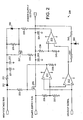
- the hold up power supply system 100 includes a diode 101, a capacitor 103, a switch 104 and a hold-up controller.
- the hold-up power supply receives power from a high voltage bus input and a power supply bus input, and provides power to flash memory through a power supply output.
- the hold-up power supply receives a hold-up signal that is used to indicate when a loss of power is about to occur.
- the hold-up signal is disabled and the switch 104 is closed. This allows power from the power supply bus to be delivered to the power supply output, providing power to the flash memory system.
- the capacitor 103 stores the power that will be used to power the flash memory in the event of a power loss on the power supply bus.
- the high voltage bus provides the high voltage that is on the capacitor 103.
- the hold-up signal When a power loss occurs, the hold-up signal is enabled. The enabling of the hold-up signal causes the switch 104 to open. This disconnects the power supply output from the now failing power supply bus.
- the hold-up controller receives the hold-up signals and controllably delivers power from the capacitor 103 to the power supply output.
- the power from capacitor 103 provides flash memory with sufficient time to finish any writes and erasures that were in progress, enabling the flash memory to shut down gracefully.
- the diode 101 prevents power from flowing from capacitor 103 back into the high voltage bus, ensuring that it will be available to power the flash memory system.
- the hold-up controller is used to controllably provide the power from the capacitor 103 to the power supply output. Specifically, the hold-up controller is used to provide the proper voltage needed to the power supply output. Because the capacitor 103 is charged by the high-voltage bus, it stores a voltage that is higher than desirable for the power supply output. The hold-up controller preferably uses feedback to provide a more desirable voltage to the power supply output.
- the power supply bus provides the power used to supply the flash memory system during normal operation.
- the power supply bus thus preferably provides a voltage compatible for powering the flash memory system.
- the power supply bus will supply between 3 and 5 volts. Of course, other voltages can be used.
- this power supply voltage can be further regulated before it is passed to the flash memory system.
- the power supply bus can supply 5 volts, which is delivered to the power supply output during normal operation.
- the supplied five volts can be further regulated to 3.3 volts before it is passed on to the flash memory system.
- the high voltage bus provides the power that is stored on capacitor 103, and is used to power the power supply output during power loss.
- the high voltage bus provides a voltage that is higher than the power supply bus voltage. This allows the capacitor 103 to store sufficient energy to power the flash memory temporarily without requiring excessive capacitor size.
- the high power bus can supply between 12 and 19 volts. As a further example, when the power supply bus provides 5 volts, the high voltage bus can provide 18.9 volts.
- the hold-up signal can be any suitable signal that is enabled when a power loss occurs, with any suitable means of detecting a power loss. It is generally desirable that the hold-up signal become enabled immediately after the power loss occurs. This allows the hold-up power supply to immediately begin to provide supplemental power, allowing the flash memory system to shut down gracefully.
- the hold-up power supply 200 includes diode 201, zener diode 203, a precision zener diode 204, FETs 205 and 207, comparators 211, 212 and 213, capacitors 221, 222, 223 and 224, and resistors 231, 232, 233, 234, 235, 236, 237, 238, 239, 240, 241 and 242.
- the hold-up power supply 200 receives power from a high voltage bus input and a power supply bus input, and provides power to flash memory through a power supply output.
- the hold-up power supply 200 receives a hold-up signal that is used to indicate when a power loss is about to occur.
- FET 205 preferably comprises an n-channel FET while FET 207 preferably comprises a p-channel FET.
- FET types are preferred for the polarity of the power supply bus and high voltage bus in this application, however, other applications may preferably use other FET types.
- other switch devices such as bipolar transistors could be used in the place of the FETs shown in FIG. 2 .
- Comparators 211, 212 and 213 preferably comprise open collector comparators such as LM139 comparators.
- Capacitors 221 and 222 store the energy needed to momentarily power the flash memory system. While hold-up power supply 200 uses two capacitors in parallel for this purpose, more or less capacitors could be used depending upon specific application requirements.
- Capacitors 223 and 234 provide control over ripple voltage at the power supply output.
- capacitors 221 and 222 can comprise 47 microfarad capacitors, while capacitor 223 comprises 560 microfarads and capacitor 224 comprises .47 microfarads.
- resistor 231 comprises a 100 ohms resistor
- resistor 232, 233, 236, 239, 240 and 241 comprise 10k ohm resistors
- resistor 237 comprises a 3.92k ohm resistor
- resistor 238 comprises a 39.2k ohm resistor
- resistors 242 and 235 comprise 1k ohm resistors
- resistor 234 comprises a 1.21 ohm resistor.
- zener diode 204 is preferably 2.5 volts.
- the hold-up signal is held low.
- the low hold-up signal is delivered to the negative input of comparator 211 and the positive input of comparator 212.
- the positive input of comparator 211 and the negative input of comparator 212 receive a voltage from the power supply bus as determined by the voltage divider comprising resistors 236 and 237.
- the voltage provided by the voltage divider is higher with respect to the low hold-up signal, and thus comparator 211 is in high impendence mode and its output floats. This allows the output of comparator 211 to be controlled by the voltage from the high voltage bus as determined by the voltage divider comprising resistors 233 and 238. This high voltage is applied to the gate of NFET 205 and turns it on.
- the power supply bus is connected to the power supply output, powering the flash memory system.
- the comparator 212 output is pulled toward ground in a low impedance state.
- the low output of comparator 212 is passed to the negative input of comparator 213, while the positive input of comparator 213 receives voltage from the power supply bus as determined by resistors 239 and 240. This causes the output of comparator 213 to be high impedance mode and its output floats.
- resistor 232 causes the gate to source voltage of PFET 207 to be near zero, turning PFET 207 off.
- the high voltage bus is disconnected from the power supply output.
- the hold-up signal goes high.
- the high hold-up signal at the negative input of comparator 211 causes the output of comparator 211 to be pulled low to ground.
- This low signal is passed to the gate of NFET 205 turning it off. This disconnects the power supply bus from the power supply output, and prevents power supplied by the hold-up power supply 200 from flowing back into the power supply bus.
- the high hold-up signal at the positive input of the comparator 212 causes the output of comparator 212 to float.
- the voltage at the negative input of comparator 213 is determined by resistors 241, 242 and zener diode 204.
- the zener diode 204 supplies a reference voltage even when the power supply output has dropped below its normal level. For example, where the power supply output is a 5 volt output, the zener diode 204 and resistors 241 and 242 will provide 2.5 volts even when the power supply output has dropped below normal levels. This voltage is used in hold-up power supply 200 as a reference voltage to determine when comparator 213 is turned on.
- the value of the zener diode 204 was chosen to be 2.5 volts to allow it be accurate even when the power supply output is much less than its nominal value of 5 volts.
- Resistor 242 supplies sufficient current to zener diode 204 to cause it to be 2.5 volts even when the power supply output has dropped to only 3.5 volts.
- the ratio of resistors 239 and 240, in conjunction with zener diode 204 thus provide a dependable reference voltage to comparator 213. This facilitates the comparator 213 properly determining the power supply output voltage during operation in the hold-up moder.
- the reference could be provided by elements other than the illustrated zener diode 204. For example, it can be provided with precision integrated circuit voltage reference such as a LT1009 voltage reference.
- the voltage provided from the power supply bus through resistors 239 and 240 to the positive input of comparator 213 may be higher or lower than the reference voltage provided by device 204 through resistor 241 to the negative input of comparator 213.
- the voltage on the power supply output will drop below the operational voltage.
- the voltage at the negative input of comparator 213 begins to exceed the voltage at the positive input of comparator 213.
- the voltage at the gate of PFET 207 is then determined by the voltage provided from the high voltage bus through resistor 232 and 235. This causes the PFET 207 to momentarily turn on, allowing current to flow from the capacitors 221 and 222 to the power supply output.
- the needed voltage to operate the flash memory is provided from capacitors 221 and 222.
- resistor 234 is used to insure that excessive current does not flow from capacitors 222 and 221 during hold up. This same result could be achieved using an inductor of appropriate size. This would have the advantage of preventing the current from changing immediately, and possibly allow the use of smaller storage capacitors.
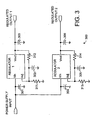
- a voltage regulator 300 is illustrated that receives a power supply input and provides two regulated outputs.
- the voltage regulator 300 uses two three-terminal regulators to provide these regulated outputs.
- the voltage regulator 300 can be configured to output two regulated 3.3 volt outputs. This allows modem flash memory systems that use this voltage to be powered off the five volt power supply input.
- different applications may require different voltage outputs and receive different voltage inputs. Other applications may not require the use of a voltage regulator 300 at all.
- voltage regulator 300 comprises two three terminal regulators, capacitors 301, 302, 303, 304, 305 and 306, and resistors 311, 312, 313, and 314.
- the capacitors 301 and 304 comprise .47 microfarads and the capacitors 302, 303, 305 and 306 comprise 47 microfarads.
- resistors 311 and 313 comprise 200 ohms
- resistors 312 and 314 comprise 121 ohms.
- the present invention thus provides hold-up power supply for flash memory systems.
- the hold-up power supply provides the flash memory with the power needed to temporarily operate when a power loss exists. This allows the flash memory system to complete any erasures and writes, and thus allows it to shut down gracefully.
- the hold-up power supply detects when a power supply loss on a power supply bus is occurring and supplies the power needed for the flash memory system to temporally operate.
- the hold-up power supply stores power in at least one capacitor. During normal operation, power from a high voltage supply bus is used to charge the storage capacitors. When a power supply loss is detected, the power supply bus is disconnected from the flash memory system.
- a hold-up controller controls the power flow from the storage capacitors to the flash memory system. The hold-up controller uses feedback to assure that the proper voltage is provided from the storage capacitors to the flash memory system. This power supplied by the storage capacitors allows the flash memory system to complete any erasures and writes, and thus allows the flash memory system to shut down gracefully.
Landscapes
- Engineering & Computer Science (AREA)
- Power Engineering (AREA)
- Techniques For Improving Reliability Of Storages (AREA)
- Read Only Memory (AREA)
- Power Sources (AREA)
Applications Claiming Priority (3)
| Application Number | Priority Date | Filing Date | Title |
|---|---|---|---|
| US186516 | 1988-04-25 | ||
| US10/186,516 US6735117B2 (en) | 2002-07-01 | 2002-07-01 | Hold-up power supply for flash memory |
| PCT/US2003/020797 WO2004003928A2 (en) | 2002-07-01 | 2003-06-30 | Backup power supply for flash memory |
Publications (2)
| Publication Number | Publication Date |
|---|---|
| EP1530795A2 EP1530795A2 (en) | 2005-05-18 |
| EP1530795B1 true EP1530795B1 (en) | 2009-04-22 |
Family
ID=29779909
Family Applications (1)
| Application Number | Title | Priority Date | Filing Date |
|---|---|---|---|
| EP03762302A Expired - Lifetime EP1530795B1 (en) | 2002-07-01 | 2003-06-30 | Hold-up power supply for flash memory |
Country Status (6)
| Country | Link |
|---|---|
| US (1) | US6735117B2 (enExample) |
| EP (1) | EP1530795B1 (enExample) |
| JP (1) | JP2005532620A (enExample) |
| AU (1) | AU2003256361A1 (enExample) |
| DE (1) | DE60327325D1 (enExample) |
| WO (1) | WO2004003928A2 (enExample) |
Families Citing this family (24)
| Publication number | Priority date | Publication date | Assignee | Title |
|---|---|---|---|---|
| JP4133166B2 (ja) * | 2002-09-25 | 2008-08-13 | 株式会社ルネサステクノロジ | 不揮発性半導体記憶装置 |
| JP4748563B2 (ja) * | 2004-12-07 | 2011-08-17 | 株式会社日立超エル・エス・アイ・システムズ | 記憶装置 |
| US7352626B1 (en) * | 2005-08-29 | 2008-04-01 | Spansion Llc | Voltage regulator with less overshoot and faster settling time |
| US7295475B2 (en) * | 2005-09-20 | 2007-11-13 | Spansion Llc | Flash memory programming using an indication bit to interpret state |
| US8358543B1 (en) | 2005-09-20 | 2013-01-22 | Spansion Llc | Flash memory programming with data dependent control of source lines |
| DE102007052107B4 (de) * | 2006-11-02 | 2017-09-21 | Hitachi, Ltd. | Elektronische Steuerungseinrichtung und Verfahren zum Eintragen von Backup-Daten in dieselbe |
| CN201075737Y (zh) | 2007-07-20 | 2008-06-18 | 忆正存储技术(深圳)有限公司 | 一种掉电保护电路 |
| JP2009181624A (ja) * | 2008-01-30 | 2009-08-13 | Panasonic Corp | 不揮発性半導体記憶装置 |
| TWI451424B (zh) * | 2009-04-17 | 2014-09-01 | Mstar Semiconductor Inc | 應用於快閃記憶體之保護電路及電源系統 |
| US8228753B2 (en) | 2009-07-29 | 2012-07-24 | Stec, Inc. | System and method of maintaining data integrity in a flash storage device |
| JP5556405B2 (ja) * | 2009-10-19 | 2014-07-23 | 株式会社リコー | 電源制御装置、画像形成装置および電源制御方法 |
| DE102010011749B4 (de) * | 2010-03-17 | 2018-05-03 | Texas Instruments Deutschland Gmbh | Elektronische Vorrichtung und Verfahren zur FRAM-Spannungsversorgungsverwaltung |
| JP5381864B2 (ja) * | 2010-03-30 | 2014-01-08 | パナソニック株式会社 | フラッシュメモリ用電源装置 |
| ITMI20111201A1 (it) * | 2011-06-29 | 2012-12-30 | St Microelectronics Srl | Sistema di controllo per dispositivo di memoria |
| US8767354B1 (en) * | 2011-12-08 | 2014-07-01 | Western Digital Technologies, Inc. | Data storage device employing cascaded voltage regulators during power failure |
| US8957655B2 (en) * | 2012-03-16 | 2015-02-17 | Micrel, Inc. | Last gasp hold-up circuit using adaptive constant on time control |
| CN103366815A (zh) * | 2012-04-06 | 2013-10-23 | 鸿富锦精密工业(深圳)有限公司 | 断电保护电路及具有该断电保护电路的电子装置 |
| CN103762966A (zh) * | 2014-01-10 | 2014-04-30 | 美的集团股份有限公司 | 掉电记忆电路及其掉电记忆方法 |
| US10497404B2 (en) * | 2014-10-03 | 2019-12-03 | Hewlett-Packard Development Company, L.P. | Clamping circuit |
| FR3041807B1 (fr) | 2015-09-24 | 2017-12-08 | Stmicroelectronics Rousset | Procede de controle d'un cycle d'ecriture de memoire de type eeprom et dispositif correspondant |
| US10521305B2 (en) | 2016-04-29 | 2019-12-31 | Toshiba Memory Corporation | Holdup time measurement for solid state drives |
| CN107402520A (zh) * | 2016-05-18 | 2017-11-28 | 佛山市顺德区美的电热电器制造有限公司 | 烹饪电器及其掉电控制方法、启动控制方法 |
| US12301745B2 (en) * | 2021-11-24 | 2025-05-13 | Visual Defence Inc. | Hybrid smart phone smart camera system based on methods and system for modifying a smart phone |
| TWI806628B (zh) * | 2022-05-25 | 2023-06-21 | 瑞昱半導體股份有限公司 | 固態硬碟控制器與電路控制器 |
Family Cites Families (6)
| Publication number | Priority date | Publication date | Assignee | Title |
|---|---|---|---|---|
| US5438549A (en) * | 1994-02-28 | 1995-08-01 | Intel Corporation | Nonvolatile memory with volatile memory buffer and a backup power supply system |
| US5608684A (en) * | 1994-10-13 | 1997-03-04 | Hewlett-Packard Company | System and method for RAM power and data backup utilizing a capacitor and ROM |
| US5768208A (en) * | 1996-06-18 | 1998-06-16 | Microchip Technology Incorporated | Fail safe non-volatile memory programming system and method therefor |
| JP3916837B2 (ja) * | 2000-03-10 | 2007-05-23 | 株式会社東芝 | 強誘電体メモリ |
| JP2002007000A (ja) * | 2000-06-27 | 2002-01-11 | Toshiba Tec Corp | 電子機器 |
| US6862651B2 (en) * | 2000-12-20 | 2005-03-01 | Microsoft Corporation | Automotive computing devices with emergency power shut down capabilities |
-
2002
- 2002-07-01 US US10/186,516 patent/US6735117B2/en not_active Expired - Lifetime
-
2003
- 2003-06-30 EP EP03762302A patent/EP1530795B1/en not_active Expired - Lifetime
- 2003-06-30 DE DE60327325T patent/DE60327325D1/de not_active Expired - Fee Related
- 2003-06-30 WO PCT/US2003/020797 patent/WO2004003928A2/en not_active Ceased
- 2003-06-30 AU AU2003256361A patent/AU2003256361A1/en not_active Abandoned
- 2003-06-30 JP JP2004518198A patent/JP2005532620A/ja active Pending
Also Published As
| Publication number | Publication date |
|---|---|
| US6735117B2 (en) | 2004-05-11 |
| JP2005532620A (ja) | 2005-10-27 |
| AU2003256361A1 (en) | 2004-01-19 |
| DE60327325D1 (de) | 2009-06-04 |
| AU2003256361A8 (en) | 2004-01-19 |
| EP1530795A2 (en) | 2005-05-18 |
| WO2004003928A3 (en) | 2004-10-28 |
| US20040001359A1 (en) | 2004-01-01 |
| WO2004003928A2 (en) | 2004-01-08 |
Similar Documents
| Publication | Publication Date | Title |
|---|---|---|
| EP1530795B1 (en) | Hold-up power supply for flash memory | |
| US20070229149A1 (en) | Voltage regulator having high voltage protection | |
| US20080068067A1 (en) | Implementation of output floating scheme for hv charge pumps | |
| KR100299254B1 (ko) | 플래시메모리용전압공급기 | |
| US10127952B2 (en) | Power control module using protection circuit for regulating backup voltage to power load during power fault | |
| CA1219676A (en) | Non-volatile memory protection circuit with microprocessor interaction | |
| US7550954B2 (en) | Method and circuit for a voltage supply for real time clock circuitry based on voltage regulated charge pump | |
| US20110043043A1 (en) | Battery backup system with sleep mode | |
| US9984762B1 (en) | Cascaded E-fuse switch circuits to control data backup in a storage device | |
| US8514649B2 (en) | Power source and power source control circuit | |
| US20200302976A1 (en) | Power delivery circuitry | |
| US20080036528A1 (en) | Charge pump circuit | |
| US6560494B1 (en) | Electronics for a shock hardened data recorder | |
| US9007847B2 (en) | Flash memory device and method for handling power failure thereof | |
| JP4989927B2 (ja) | 負電位放電回路 | |
| EP0130760A2 (en) | Non-volatile data stores | |
| Ott | Hold-up power supply for flash memory | |
| US12407162B2 (en) | Power supply control system and processing method | |
| CN107408828A (zh) | 控制车辆的电路的电力供应的包含电池和相关组件的设备 | |
| US7388356B2 (en) | System and method for providing voltage regulation in a multi-voltage power system | |
| US20090059455A1 (en) | Method and apparatus for power interruption protection | |
| KR20100111010A (ko) | 전압 제공 회로 및 이를 구비한 반도체 장치 | |
| US7348832B2 (en) | Dual-voltage generation system | |
| CN113544621B (zh) | 低压降调节器中的功率泄漏阻断 | |
| KR20250107456A (ko) | 차량 제어 장치 및 방법 |
Legal Events
| Date | Code | Title | Description |
|---|---|---|---|
| PUAI | Public reference made under article 153(3) epc to a published international application that has entered the european phase |
Free format text: ORIGINAL CODE: 0009012 |
|
| 17P | Request for examination filed |
Effective date: 20041222 |
|
| AK | Designated contracting states |
Kind code of ref document: A2 Designated state(s): AT BE BG CH CY CZ DE DK EE ES FI FR GB GR HU IE IT LI LU MC NL PT RO SE SI SK TR |
|
| RBV | Designated contracting states (corrected) |
Designated state(s): DE GB |
|
| 17Q | First examination report despatched |
Effective date: 20070702 |
|
| GRAP | Despatch of communication of intention to grant a patent |
Free format text: ORIGINAL CODE: EPIDOSNIGR1 |
|
| GRAS | Grant fee paid |
Free format text: ORIGINAL CODE: EPIDOSNIGR3 |
|
| GRAA | (expected) grant |
Free format text: ORIGINAL CODE: 0009210 |
|
| AK | Designated contracting states |
Kind code of ref document: B1 Designated state(s): DE GB |
|
| REG | Reference to a national code |
Ref country code: GB Ref legal event code: FG4D |
|
| REF | Corresponds to: |
Ref document number: 60327325 Country of ref document: DE Date of ref document: 20090604 Kind code of ref document: P |
|
| PLBE | No opposition filed within time limit |
Free format text: ORIGINAL CODE: 0009261 |
|
| STAA | Information on the status of an ep patent application or granted ep patent |
Free format text: STATUS: NO OPPOSITION FILED WITHIN TIME LIMIT |
|
| GBPC | Gb: european patent ceased through non-payment of renewal fee |
Effective date: 20090722 |
|
| 26N | No opposition filed |
Effective date: 20100125 |
|
| PG25 | Lapsed in a contracting state [announced via postgrant information from national office to epo] |
Ref country code: GB Free format text: LAPSE BECAUSE OF NON-PAYMENT OF DUE FEES Effective date: 20090722 |
|
| PG25 | Lapsed in a contracting state [announced via postgrant information from national office to epo] |
Ref country code: DE Free format text: LAPSE BECAUSE OF NON-PAYMENT OF DUE FEES Effective date: 20100101 |