EP1530088B1 - Lithographic apparatus - Google Patents
Lithographic apparatus Download PDFInfo
- Publication number
- EP1530088B1 EP1530088B1 EP04077933A EP04077933A EP1530088B1 EP 1530088 B1 EP1530088 B1 EP 1530088B1 EP 04077933 A EP04077933 A EP 04077933A EP 04077933 A EP04077933 A EP 04077933A EP 1530088 B1 EP1530088 B1 EP 1530088B1
- Authority
- EP
- European Patent Office
- Prior art keywords
- support
- article
- zone
- lithographic apparatus
- gas
- Prior art date
- Legal status (The legal status is an assumption and is not a legal conclusion. Google has not performed a legal analysis and makes no representation as to the accuracy of the status listed.)
- Expired - Lifetime
Links
Images


Classifications
-
- G—PHYSICS
- G03—PHOTOGRAPHY; CINEMATOGRAPHY; ANALOGOUS TECHNIQUES USING WAVES OTHER THAN OPTICAL WAVES; ELECTROGRAPHY; HOLOGRAPHY
- G03F—PHOTOMECHANICAL PRODUCTION OF TEXTURED OR PATTERNED SURFACES, e.g. FOR PRINTING, FOR PROCESSING OF SEMICONDUCTOR DEVICES; MATERIALS THEREFOR; ORIGINALS THEREFOR; APPARATUS SPECIALLY ADAPTED THEREFOR
- G03F7/00—Photomechanical, e.g. photolithographic, production of textured or patterned surfaces, e.g. printing surfaces; Materials therefor, e.g. comprising photoresists; Apparatus specially adapted therefor
- G03F7/70—Microphotolithographic exposure; Apparatus therefor
- G03F7/70691—Handling of masks or workpieces
- G03F7/707—Chucks, e.g. chucking or un-chucking operations or structural details
- G03F7/70708—Chucks, e.g. chucking or un-chucking operations or structural details being electrostatic; Electrostatically deformable vacuum chucks
-
- G—PHYSICS
- G03—PHOTOGRAPHY; CINEMATOGRAPHY; ANALOGOUS TECHNIQUES USING WAVES OTHER THAN OPTICAL WAVES; ELECTROGRAPHY; HOLOGRAPHY
- G03F—PHOTOMECHANICAL PRODUCTION OF TEXTURED OR PATTERNED SURFACES, e.g. FOR PRINTING, FOR PROCESSING OF SEMICONDUCTOR DEVICES; MATERIALS THEREFOR; ORIGINALS THEREFOR; APPARATUS SPECIALLY ADAPTED THEREFOR
- G03F7/00—Photomechanical, e.g. photolithographic, production of textured or patterned surfaces, e.g. printing surfaces; Materials therefor, e.g. comprising photoresists; Apparatus specially adapted therefor
- G03F7/70—Microphotolithographic exposure; Apparatus therefor
- G03F7/70691—Handling of masks or workpieces
- G03F7/707—Chucks, e.g. chucking or un-chucking operations or structural details
-
- G—PHYSICS
- G03—PHOTOGRAPHY; CINEMATOGRAPHY; ANALOGOUS TECHNIQUES USING WAVES OTHER THAN OPTICAL WAVES; ELECTROGRAPHY; HOLOGRAPHY
- G03F—PHOTOMECHANICAL PRODUCTION OF TEXTURED OR PATTERNED SURFACES, e.g. FOR PRINTING, FOR PROCESSING OF SEMICONDUCTOR DEVICES; MATERIALS THEREFOR; ORIGINALS THEREFOR; APPARATUS SPECIALLY ADAPTED THEREFOR
- G03F7/00—Photomechanical, e.g. photolithographic, production of textured or patterned surfaces, e.g. printing surfaces; Materials therefor, e.g. comprising photoresists; Apparatus specially adapted therefor
- G03F7/70—Microphotolithographic exposure; Apparatus therefor
- G03F7/70691—Handling of masks or workpieces
- G03F7/70783—Handling stress or warp of chucks, masks or workpieces, e.g. to compensate for imaging errors or considerations related to warpage of masks or workpieces due to their own weight
-
- G—PHYSICS
- G03—PHOTOGRAPHY; CINEMATOGRAPHY; ANALOGOUS TECHNIQUES USING WAVES OTHER THAN OPTICAL WAVES; ELECTROGRAPHY; HOLOGRAPHY
- G03F—PHOTOMECHANICAL PRODUCTION OF TEXTURED OR PATTERNED SURFACES, e.g. FOR PRINTING, FOR PROCESSING OF SEMICONDUCTOR DEVICES; MATERIALS THEREFOR; ORIGINALS THEREFOR; APPARATUS SPECIALLY ADAPTED THEREFOR
- G03F7/00—Photomechanical, e.g. photolithographic, production of textured or patterned surfaces, e.g. printing surfaces; Materials therefor, e.g. comprising photoresists; Apparatus specially adapted therefor
- G03F7/70—Microphotolithographic exposure; Apparatus therefor
- G03F7/708—Construction of apparatus, e.g. environment aspects, hygiene aspects or materials
-
- H—ELECTRICITY
- H10—SEMICONDUCTOR DEVICES; ELECTRIC SOLID-STATE DEVICES NOT OTHERWISE PROVIDED FOR
- H10P—GENERIC PROCESSES OR APPARATUS FOR THE MANUFACTURE OR TREATMENT OF DEVICES COVERED BY CLASS H10
- H10P72/00—Handling or holding of wafers, substrates or devices during manufacture or treatment thereof
- H10P72/04—Apparatus for manufacture or treatment
- H10P72/0431—Apparatus for thermal treatment
- H10P72/0432—Apparatus for thermal treatment mainly by conduction
Definitions
- the present invention relates to a lithographic apparatus and a device manufacturing method. More specifically, the invention relates to a lithographic apparatus comprising:
- a lithographic apparatus is a machine that applies a desired pattern onto a target portion of a substrate.
- Lithographic apparatus can be used, for example, in the manufacture of integrated circuits (ICs).
- a patterning means such as a mask, may be used to generate a circuit pattern corresponding to an individual layer of the IC, and this pattern can be imaged onto a target portion (e.g. comprising part of, one or several dies) on a substrate (e.g. a silicon wafer) that has a layer of radiation-sensitive material (resist).
- a single substrate will contain a network of adjacent target portions that are successively exposed.
- lithographic apparatus include so-called steppers, in which each target portion is irradiated by exposing an entire pattern onto the target portion in one go, and so-called scanners, in which each target portion is irradiated by scanning the pattern through the projection beam in a given direction (the "scanning"-direction) while synchronously scanning the substrate parallel or anti-parallel to this direction.
- an article such as a wafer or reticle is clamped on an article support by a clamping force, that may range from vacuum pressure forces, electrostatic forces, intermolecular binding forces or just gravity force.
- the article support defines a plane, in the form of a plurality of protrusions defining an even flat surface on which the wafer or reticle is held. Tiny variations in the height of these protrusions are detrimental to image resolution, since a small deflection of the article from an ideal plane orientation may result in rotation of the wafer and a resulting overlay error due to this rotation.
- height variations of the article support may result in height variation of the article that is supported thereby. During the lithographic process, such height variations may affect image resolution due to a limited focal distance of the projection system. Therefore it is very critical to have an ideal flat article support.
- European patent application EP0947884 describes a lithographic apparatus having a substrate holder wherein protrusions are arranged to improve the flatness of the substrate. These protrusions have a general diameter of 0.5 mm and are located generally at a distance of 3 mm away from each other and thereby form a bed of supporting members that support the substrate. The height of the protrusions lies in the range 1 mu m - 15 mu m. Due to the relative large spaces in between the protrusions, contaminations possibly present generally do not form an obstruction for the flatness of the substrate, since these will be lying in between the protrusions and will not lift the substrate locally.
- the said "article” may be any of the above mentioned terms wafer, reticle, mask, or substrate, more specifically terms such as
- the EUV-lithography which uses a projection beam in the Extreme UltraViolet area, therefore operates in (near) vacuum conditions in order to allow to pass the projection beam of radiation substantially unhindered to the article to be placed in said beam.
- vacuum pressure is relative to particular gasses that are present in the environment.
- the allowable background pressure is very low, in the order of 1e-9 - 1e-12 millibar.
- the requirements are less strict, for instance, for Ar an allowable background pressure ranges from 1e-4 mbar - 1e-2 mbar, in particular, a pressure of 1e-3 mbar.
- the relative background pressure may vary in terms of the environment of the apparatus. For instance, where the article support functions in the environment of a wafer support, the vacuum requirements for certain components may be less strict than in the environment where the article support functions as a reticle support.
- the partial pressures for contaminants may differ a factor 100 between optics compartment (including reticle support) and wafer compartment and are much lower than the total pressure (typical numbers are 1e-9 to 1e-12 mbar).
- the article support will further, if necessary, be provided with cooling means such as cooling ducts having cooling media etc.
- the conventional approach is providing a so-called "hard rim", which is a boundary wall substantially sealing of the backfill gas from the vacuum by forming a gas seal between the bottom side of the article and the upper side of the article support.
- a sealing rim provides additional support to carry the article. Such additional support disturbs the pressure load of the article, which may cause local bending of the article. Such bending introduces rotation of the article surface, which may cause overlay effects that are undesired.
- a sealing rim provides almost a doubling of increase of contact area between the article and article support. This is undesirable since it is an aim to minimize such contact area in order to prevent contamination particles to come in between the contact zones, creating unevenness of support and corresponding bending problems of the article.
- the invention has as an object to provide a lithographic apparatus where the above mentioned problems are overcome and wherein a backfill gas supply is provided which does not suffer from the above mentioned drawbacks.
- This object is achieved by a lithographic apparatus according to the features of claim 1.
- EP09859976 which is considered the closest prior art to the subject-matter of claim 1, discloses an EUV lithographic scanning apparatus comprising a movable article support for supporting a flat article and an electrostatic chuck.
- US2002/0159217 discloses a support having a plurality of protrusions defining a support zone and further comprising backfill gas discharge zones arranged in the support zone and arranged near the border of the support zone and central to the support zone respectively, the gas discharge zones being connected by gas flow channels buried in the article support or open troughs positioned at predetermined positions in the support in the supporting zone.
- US 2003/0127605 A discloses a scanning lithography apparatus comprising a vacuum chuck ( Figure 2).
- the vacuum chuck comprises gas discharge zones connected by channels (88) buried in the chuck.
- a backfill gas discharge is provided wherein selected positions, preferably along all positions along a perimeter of the support area, are put on a predetermined backfill gas pressure.
- the resultant backfill gas flow will in steady state have filled the enclosed area, thus providing a substantially constant backfill gas pressure in said area, resulting in uniform thermal conductivity properties in said area.
- said discharge zone has a reduced gas flow resistance relative to a gas flow resistance between said article and said article support.
- a gas feed channel towards the discharge zone may be designed to have a reduced flow impedance, resulting in a short waiting time where the backfill gas fills the backside of the article.
- said discharge zone may be formed by a concentric gas feed trough.
- said discharge zone may be formed by a annular recess close to the perimeter of the support area. Said annular recess forms a trough, which is bounded by the article when supported by the article support.
- said discharge zone may comprises a plurality of spaced apart gas feeds.
- said spaced apart gas feeds may be formed by gas channel openings that form a regular concentric pattern of arranged close to the boundary of the support area.
- the article extends beyond the hard rim.
- no thermal conductivity is provided due to the absence of backfill gas.
- thermal conductivity is provided which provides improved thermal conductivity in the boundary zone of the article.
- Said support zone may not be bounded by a hard-rim seal, or may not be bounded by a boundary wall at all. Since the discharge zone is positioned near the boundary said support zone, in only a small fraction of the support zone the backfill gas pressure drops, to eventually the (vacuum) pressure conditions that are present in the lithographic apparatus. Hence it follows that the seal configuration can be dispensed with, resulting in better leveling properties of the article support. In some designs, it may be beneficial to have some sort of seal, in particular a "non-contact" seal, or "leaking" seal, forming an increased flow resistance contact” seal, or "leaking” seal, forming an increased flow resistance to limit the gas flow and increase the gas pressure near the boundary of the article.
- said support zone is bounded by a boundary wall defining a boundary wall height that lies below said plane of support.
- the backfill gas is an inert gas, such as Argon.
- the allowable background pressure of the vacuum surrounding is relative high and a leaking rate of less than 1 mbar*l/s, in particular 0.15 mbar*l/s, is acceptable for Argon as a backfill gas, depending on the relative position of the article support.
- the leaking rate was calculated to be 0.12 mbar*l/s, which was found to be within the above indicated upper limit.
- the calculated leak rate was 3e-3 mbar*l/s, which is far within above maximum specification.
- a lithographic apparatus comprising a vacuum pump system for providing a vacuum pressure for operating said lithographic apparatus in vacuum pressure conditions, said vacuum pump operating to eliminate backfill gas flowing from the backside of said article.
- the vacuum pump in particular, a vacuum turbo pump, is simply operated to remove the leaking backfill gas.
- a vacuum turbo pump is simply operated to remove the leaking backfill gas.
- said vacuum pump system comprises a suction zone enclosing said support zone.
- escaping back fill gas particles may be captured directly before possibly adversely affecting the illumination process.
- lithographic apparatus in the manufacture of ICs, it should be understood that the lithographic apparatus described herein may have other applications, such as the manufacture of integrated optical systems, guidance and detection patterns for magnetic domain memories, liquid-crystal displays (LCDs), thin-film magnetic heads, etc.
- LCDs liquid-crystal displays
- any use of the terms “wafer” or “die” herein may be considered as synonymous with the more general terms “substrate” or "target portion”, respectively.
- the substrate referred to herein may be processed, before or after exposure, in for example a track (a tool that typically applies a layer of resist to a substrate and develops the exposed resist) or a metrology or inspection tool.
- the disclosure herein may be applied to such and other substrate processing tools.
- the substrate may be processed more than once, for example in order to create a multi-layer IC, so that the term substrate used herein may also refer to a substrate that already contains multiple processed layers.
- radiation and “beam” used herein encompass extreme ultra-violet (EUV) radiation (e.g. having a wavelength in the range of 5-20 nm).
- EUV extreme ultra-violet
- patterning means used herein should be broadly interpreted as referring to means that can be used to impart a projection beam with a pattern in its cross-section such as to create a pattern in a target portion of the substrate. It should be noted that the pattern imparted to the projection beam may not exactly correspond to the desired pattern in the target portion of the substrate. Generally, the pattern imparted to the projection beam will correspond to a particular functional layer in a device being created in the target portion, such as an integrated circuit.
- Patterning means may be transmissive or reflective.
- Examples of patterning means include masks, programmable mirror arrays, and programmable LCD panels.
- Masks are well known in lithography, and include mask types such as binary, alternating phase-shift, and attenuated phase-shift, as well as various hybrid mask types.
- An example of a programmable mirror array employs a matrix arrangement of small mirrors, each of which can be individually tilted so as to reflect an incoming radiation beam in different directions; in this manner, the reflected beam is patterned.
- the support structure may be a frame or table, for example, which may be fixed or movable as required and which may ensure that the patterning means is at a desired position, for example with respect to the projection system. Any use of the terms "reticle” or “mask” herein may be considered synonymous with the more general term "patterning means”.
- projection system used herein should be interpreted as encompassing reflective optical systems. Any use of the term “lens” herein may be considered as synonymous with the more general term “projection system”.
- the illumination system may encompass various types of reflective optical components for directing, shaping, or controlling the projection beam of radiation, and such components may also be referred to below, collectively or singularly, as a "lens”.
- the lithographic apparatus may be of a type having two (dual stage) or more substrate tables (and/or two or more mask tables). In such "multiple stage” machines the additional tables may be used in parallel, or preparatory steps may be carried out on one or more tables while one or more other tables are being used for exposure.
- Figure 1 schematically depicts a lithographic apparatus according to a particular embodiment of the invention.
- the apparatus comprises:
- the apparatus is of a reflective type (e.g. employing a reflective mask or a programmable mirror array of a type as referred to above).
- the illuminator IL receives a beam of radiation from a radiation source SO.
- the source and the lithographic apparatus may be separate entities, for example when the source is a plasma discharge source. In such cases, the source is not considered to form part of the lithographic apparatus and the radiation beam is generally passed from the source SO to the illuminator IL with the aid of a radiation collector comprising for example suitable collecting mirrors and/or a spectral purity filter. In other cases the source may be integral part of the apparatus, for example when the source is a mercury lamp.
- the source SO and the illuminator IL may be referred to as a radiation system.
- the illuminator IL may comprise adjusting means for adjusting the angular intensity distribution of the beam.
- adjusting means for adjusting the angular intensity distribution of the beam Generally, at least the outer and/or inner radial extent (commonly referred to as ⁇ -outer and ⁇ -inner, respectively) of the intensity distribution in a pupil plane of the illuminator can be adjusted.
- the illuminator provides a conditioned beam of radiation, referred to as the projection beam PB, having a desired uniformity and intensity distribution in its cross -section.
- the projection beam PB is incident on the mask MA, which is held on the mask table MT. Being reflected by the mask MA, the projection beam PB passes through the lens PL, which focuses the beam onto a target portion C of the substrate W.
- the substrate table WT can be moved accurately, e.g. so as to position different target portions C in the path of the beam PB.
- the first positioning means PM and position sensor IF1 can be used to accurately position the mask MA with respect to the path of the beam PB, e.g. after mechanical retrieval from a mask library, or during a scan.
- movement of the object tables MT and WT will be realized with the aid of a long-stroke module (coarse positioning) and a short-stroke module (fine positioning), which form part of the positioning means PM and PW.
- Mask MA and substrate W may be aligned using mask alignment marks M1, M2 and substrate alignment marks P1, P2.
- the depicted apparatus can be used in the following modes:
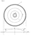
- Figure 2 depicts a prior-art embodiment of an article support 1.
- the article support 1 is for supporting a wafer, shortly to be called wafer support table, and generally circular in form, which is common for wafer support tables.
- the article support may also be of another shape, in particular, a square shape.
- the wafer support table 1 comprises a plurality of protrusions 2 that are dimensioned to provide a flat support for supporting a wafer (not shown).
- the protrusions 2 thereby define a support zone 3.
- the boundary of said support zone 3 is formed by a surrounding wall 4, which forms a seal for confining backfill gas (not shown).
- the surrounding wall 4 is of the same height as the supporting protrusions 2 and thereby forms a supporting element for also supporting the wafer.
- This type of support is indicated as a "hard-rim" seal since the boundary wall 4 physically contacts the wafer during sealing and presses the bottom side thereof. This causes the wafer to deform and unevenness is introduced in the support of the wafer, so that the wafer surface to be irradiated is not perfectly flat.
- backfill gas is introduced via gas feeds 5 which are located at selected positions, usually nearby the center of the wafer support table 1, or somewhere slightly off center as depicted in fig. 1.
- gas feeds 5 which are located at selected positions, usually nearby the center of the wafer support table 1, or somewhere slightly off center as depicted in fig. 1.
- the feeds are indicated by closed circles or thick lines.
- the backfill-gas pressure expands from the positions of the feeds 5, which is schematically indicated in the associated corresponding pressure diagram schematically depicting a backfill gas pressure P as a relation of radial position S from the center of the wafer support table (arbitrary units).
- a bell-shaped pressure curve I expands to a fully expanded, substantially even gas pressure II in the support zone 3, confined by the sealing rim 4.
- Outside sealing rim 4 there is no backfill gas and consequently no backfill gas pressure; consequentially there is no thermal conduction in the outer zone of the wafer support table 1, leading to adversary effects such as local thermal expansion, which is detrimental to image resolution and even degrading of the wafer and/or wafer support table 1.
- Figure 3 shows a first example of the article support 1 not forming part of the invention.
- the shown example is in the form of a wafer support table 1, of a substantially circular form.
- the supporting zone 3 is not bounded by a hard-rim seal but by a leaking seal 6.
- This leaking seal 6 may even be absent, provided that the flow characteristics of the backfill gas pressure, in relation to the feed positions is such that a sufficient pressure can be built up in the presence of the ambient pressure, which is often a vacuum pressure.
- the boundary gas feeds 7 are forming a gas discharge zone that substantially enclose said support zone 3 since they are positioned near the border thereof.
- the gas feeds 5 are positioned near the boundary distanced from 1-40 %, preferably from 1-15%, even more preferably, 1-5% away from the boundary 6 relative to a radial distance of the wafer support table 1.
- the positions of the gas feeds 7 are as far to the boundary 6 as possible, without compromising the gas inflow to the center of the wafer support table 1 too much or the gas outflow from under the wafer too much.
- the backfill-gas pressure expands from the feeds 7, which is schematically indicated in the associated corresponding pressure diagram schematically depicting a backfill gas pressure P as a relation of radial position S from the center of the wafer support table (arbitrary units).
- the backfill gas pressure in the support zone 3 is maintained on said same predetermined level II' as well.
- the pressure curve expands from the boundaries of the supporting zone to a full spread over the whole supporting zone 3 as indicated by pressure level 1'. Due to gas outflow through the leaking seal zone 6, the pressure drops to a zero level substantially further away from the center as in the hard-seal configuration depicted in Figure 1, providing better thermal conduction in the boundary zone of the wafer.
- the adversary effects as discussed with reference to Figure 1 are overcome and a better image resolution can be provided near the boundaries of the wafer.
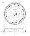
- Figure 4 shows another example not forming part of the invention where central feeds 5 are added in addition to the boundary feeds 7.
- the presence of such central feeds 5 is beneficial in that the steady state configuration with reference to Figure 3 is reached faster. Once reached, the gas outflow in said central feeds 5 may be shut off.
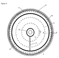
- Figure 5 shows an article support 1 according to an embodiment of the invention where the gas feeds are formed by troughs, that are positioned at predetermined positions in the supporting zone 3. At least one of said through substantially encloses the supporting zone, as indicated by the outer trough 8.
- the troughs are in gas feeding connection with each other, as indicated by a linking channel 9.
- Such channels may open, forming a linking trough 9.
- Such channels 9 may also be buried in the article support and only at the ends thereof forming open connections to the backfill gas feeding zone 8 and other, more interior zone(s) 10.
- a further trough 11 may be present adjacent to the leaking boundary seal 6. Such a trough 11 may form an improved blockade for the outflow of gas through the boundary seal 6 in the molecular flow regime.
- Figure 6 shows a schematic height map of the article support 1 along the lines X-X depicted in Figure 5.
- a wafer 12 is positioned on top of the protrusions 2 (for clarity's sake depicted with a slight gap therebetween).
- the height of the protrusions 2 is a conventional height of approximately 5 mu m, whereas the leaking seal 6 is lowered to that height by an amount of 0.1-5 mu m. It is noted that in an optimized configuration, the leaking seal 6 may be altogether absent.
- a gas feed trough 9 is present between the last row 13 and second last row 14 of protrusions 2. Between the leaking seal and the outer row 13, a further trough 11 is present. Directly outside of the wafer support, a suction pump 15 may be present to trap outflowing gas. Schematically indicated is the flow path of a gas particle in the molecular flow regime. Due to the presence of the trough 11, an increased impedance to gas outflow may be formed.
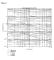
- Figure 7 illustrates the leak rates that are calculated depending on a particular geometry of the boundary wall for a standard wafer having a circumference of 942 mm.
- This geometry comprises a boundary wall that has a lowered seal (indicated as "gap") of 200; 500;1000;2000 and 5000 nm.
- the leak rate increases with the gap width, so that the lower line in the chart corresponds to the lowest value and the upper line in the chart corresponds to the highest value of the gap.
- the gap width corresponding to the distance of the boundary wall 6 to the gas supply feed 7, ranges from 0.1 mm to 10 mm. It is shown that in the indicated ranges, the leaking rate, expressed in mbar*liters/second varies from 0.5 e-4 to close to 1.
- the leakrate of the backfill gas into the stage compartment should be less than 1 mbar*liter/s, more preferably less than 0.1 mbar*liter/s, most preferably less than 1e-5 mbar*liter/s.
- the leaking rate is about 0.12 mbar*l/s, well within said specified maximum leak rate.
- These values are for an applied (total) background pressure of about 1 e-3 mbar. When the background pressure of the vacuum environment is lower, the leaking rate will be lowered correspondingly.
- the leakrate of the backfill gas into the stage compartment should be less than 0.01 mbar*liter/s, more preferably less than 1e-3 mbar*liter/s, most preferably less than 1e-7 mbar*liter/s.
- the gap may be as much as 5 um.
- a preferred embodiment for a wafer comprised a gap of 500 nm and 0.5 mm width, giving rise to a leakrate of 3e-3 mbar*l/s.
- such an embodiment comprises a gap width of 2 mm and a gap of 200 nm for a total circumference of 1136 mm.
- the invention has been illustrated with reference to an article support that is substantially circular and that is used for supporting a wafer to be illuminated by the projection beam.
- the invention may as well be applied to any other article, in particular, to an article in the form of a reticle.
Landscapes
- Physics & Mathematics (AREA)
- General Physics & Mathematics (AREA)
- Health & Medical Sciences (AREA)
- Engineering & Computer Science (AREA)
- Environmental & Geological Engineering (AREA)
- Epidemiology (AREA)
- Public Health (AREA)
- Exposure And Positioning Against Photoresist Photosensitive Materials (AREA)
- Exposure Of Semiconductors, Excluding Electron Or Ion Beam Exposure (AREA)
- Container, Conveyance, Adherence, Positioning, Of Wafer (AREA)
Priority Applications (1)
| Application Number | Priority Date | Filing Date | Title |
|---|---|---|---|
| EP04077933A EP1530088B1 (en) | 2003-11-05 | 2004-10-25 | Lithographic apparatus |
Applications Claiming Priority (3)
| Application Number | Priority Date | Filing Date | Title |
|---|---|---|---|
| EP03078504 | 2003-11-05 | ||
| EP03078504 | 2003-11-05 | ||
| EP04077933A EP1530088B1 (en) | 2003-11-05 | 2004-10-25 | Lithographic apparatus |
Publications (2)
| Publication Number | Publication Date |
|---|---|
| EP1530088A1 EP1530088A1 (en) | 2005-05-11 |
| EP1530088B1 true EP1530088B1 (en) | 2007-08-08 |
Family
ID=34626394
Family Applications (1)
| Application Number | Title | Priority Date | Filing Date |
|---|---|---|---|
| EP04077933A Expired - Lifetime EP1530088B1 (en) | 2003-11-05 | 2004-10-25 | Lithographic apparatus |
Country Status (8)
| Country | Link |
|---|---|
| US (1) | US7307696B2 (enExample) |
| EP (1) | EP1530088B1 (enExample) |
| JP (1) | JP4451280B2 (enExample) |
| KR (1) | KR100700372B1 (enExample) |
| CN (1) | CN100504607C (enExample) |
| DE (1) | DE602004008009T2 (enExample) |
| SG (1) | SG111314A1 (enExample) |
| TW (1) | TW200527153A (enExample) |
Families Citing this family (24)
| Publication number | Priority date | Publication date | Assignee | Title |
|---|---|---|---|---|
| CN100382275C (zh) * | 2004-10-29 | 2008-04-16 | 东京毅力科创株式会社 | 基板载置台、基板处理装置及基板的温度控制方法 |
| US7834974B2 (en) | 2005-06-28 | 2010-11-16 | Asml Netherlands B.V. | Lithographic apparatus and device manufacturing method |
| US7978308B2 (en) * | 2006-05-15 | 2011-07-12 | Asml Netherlands B.V. | Lithographic apparatus and device manufacturing method |
| US7593096B2 (en) | 2006-05-15 | 2009-09-22 | Asml Netherlands B.V. | Lithographic apparatus and device manufacturing method |
| WO2008013443A2 (en) * | 2006-07-28 | 2008-01-31 | Mapper Lithography Ip B.V. | Lithography system, method of heat dissipation and frame |
| US8705010B2 (en) | 2007-07-13 | 2014-04-22 | Mapper Lithography Ip B.V. | Lithography system, method of clamping and wafer table |
| JP5866323B2 (ja) * | 2007-07-13 | 2016-02-17 | マッパー・リソグラフィー・アイピー・ビー.ブイ. | リソグラフィシステム、クランプ方法及びウェーハテーブル |
| TWI450047B (zh) * | 2007-07-13 | 2014-08-21 | 瑪波微影Ip公司 | 微影系統、夾緊方法及晶圓台 |
| JP5529865B2 (ja) * | 2008-08-08 | 2014-06-25 | エーエスエムエル ネザーランズ ビー.ブイ. | 温度安定化システム、リソグラフィ投影装置、および温度制御方法 |
| JP6099883B2 (ja) * | 2011-05-24 | 2017-03-22 | エーエスエムエル ネザーランズ ビー.ブイ. | リソグラフィ装置及び部品 |
| NL2008980A (en) | 2011-07-11 | 2013-01-14 | Asml Netherlands Bv | A fluid handling structure, a lithographic apparatus and a device manufacturing method. |
| JP5778093B2 (ja) * | 2011-08-10 | 2015-09-16 | エーエスエムエル ネザーランズ ビー.ブイ. | 基板テーブルアセンブリ、液浸リソグラフィ装置及びデバイス製造方法 |
| NL2009189A (en) | 2011-08-17 | 2013-02-19 | Asml Netherlands Bv | Support table for a lithographic apparatus, lithographic apparatus and device manufacturing method. |
| WO2014084060A1 (ja) * | 2012-11-28 | 2014-06-05 | 京セラ株式会社 | 載置用部材およびその製造方法 |
| WO2015032588A1 (en) * | 2013-09-06 | 2015-03-12 | Asml Netherlands B.V. | Methodology to generate guiding templates for directed self-assembly |
| CN105683839B (zh) | 2013-09-27 | 2017-08-08 | Asml荷兰有限公司 | 用于光刻设备的支撑台、光刻设备以及器件制造方法 |
| EP3073521B1 (en) | 2013-11-22 | 2022-04-20 | Kyocera Corporation | Electrostatic chuck |
| EP3137945B1 (en) * | 2014-04-30 | 2020-05-06 | ASML Netherlands B.V. | Support table for a lithographic apparatus, lithographic apparatus and device manufacturing method |
| CN110068991B (zh) | 2014-10-23 | 2021-03-12 | Asml荷兰有限公司 | 用于光刻设备的支撑台和光刻设备 |
| WO2017054991A1 (en) * | 2015-09-28 | 2017-04-06 | Asml Netherlands B.V. | A substrate holder, a lithographic apparatus and method of manufacturing devices |
| NL2017698A (en) | 2015-12-15 | 2017-06-26 | Asml Netherlands Bv | A Substrate Holder, a Lithographic Apparatus and Method of Manufacturing Devices |
| CN111448647B (zh) | 2018-03-26 | 2023-08-01 | 日本碍子株式会社 | 静电卡盘加热器 |
| WO2020135971A1 (en) * | 2018-12-28 | 2020-07-02 | Asml Netherlands B.V. | Substrate holder for use in a lithographic apparatus and a method of manufacturing a substrate holder |
| EP3851916A1 (en) | 2020-01-17 | 2021-07-21 | ASML Netherlands B.V. | Suction clamp, object handler, stage apparatus and lithographic apparatus |
Citations (5)
| Publication number | Priority date | Publication date | Assignee | Title |
|---|---|---|---|---|
| WO1998014999A1 (en) * | 1996-09-30 | 1998-04-09 | Lam Research Corporation | Variable high temperature chuck for high density plasma chemical vapor deposition |
| EP0985976A2 (en) * | 1998-09-08 | 2000-03-15 | Nikon Corporation | Illumination apparatus, projection exposure apparatus and projection exposure method |
| EP1119040A2 (en) * | 2000-01-20 | 2001-07-25 | Ngk Insulators, Ltd. | Electrostatic wafer chuck |
| US20020159217A1 (en) * | 2001-01-29 | 2002-10-31 | Ngk Insulators, Ltd. | Electrostatic chuck and substrate processing apparatus |
| US20030127605A1 (en) * | 2001-12-20 | 2003-07-10 | Nikon Corporation | Substrate holding unit, exposure apparatus, and device manufacturing method |
Family Cites Families (10)
| Publication number | Priority date | Publication date | Assignee | Title |
|---|---|---|---|---|
| JPH09172055A (ja) * | 1995-12-19 | 1997-06-30 | Fujitsu Ltd | 静電チャック及びウエハの吸着方法 |
| JP3814359B2 (ja) * | 1996-03-12 | 2006-08-30 | キヤノン株式会社 | X線投影露光装置及びデバイス製造方法 |
| US6033478A (en) * | 1996-11-05 | 2000-03-07 | Applied Materials, Inc. | Wafer support with improved temperature control |
| US5997963A (en) * | 1998-05-05 | 1999-12-07 | Ultratech Stepper, Inc. | Microchamber |
| JP3983387B2 (ja) * | 1998-09-29 | 2007-09-26 | 日本碍子株式会社 | 静電チャック |
| US6570752B2 (en) * | 1999-12-28 | 2003-05-27 | Nikon Corporation | Wafer chucks and the like including substrate-adhesion detection and adhesion correction |
| EP1291910B1 (en) * | 2000-01-28 | 2007-01-10 | Hitachi Tokyo Electronics Co., Ltd. | Wafer chuck, exposure system, and method of manufacturing semiconductor device |
| JP2001332609A (ja) * | 2000-03-13 | 2001-11-30 | Nikon Corp | 基板保持装置及び露光装置 |
| US6628503B2 (en) * | 2001-03-13 | 2003-09-30 | Nikon Corporation | Gas cooled electrostatic pin chuck for vacuum applications |
| US6905984B2 (en) * | 2003-10-10 | 2005-06-14 | Axcelis Technologies, Inc. | MEMS based contact conductivity electrostatic chuck |
-
2004
- 2004-10-25 DE DE602004008009T patent/DE602004008009T2/de not_active Expired - Lifetime
- 2004-10-25 EP EP04077933A patent/EP1530088B1/en not_active Expired - Lifetime
- 2004-11-02 SG SG200407087A patent/SG111314A1/en unknown
- 2004-11-04 US US10/980,833 patent/US7307696B2/en not_active Expired - Fee Related
- 2004-11-04 CN CNB2004100903705A patent/CN100504607C/zh not_active Expired - Fee Related
- 2004-11-04 KR KR1020040089338A patent/KR100700372B1/ko not_active Expired - Fee Related
- 2004-11-04 TW TW093133668A patent/TW200527153A/zh not_active IP Right Cessation
- 2004-11-05 JP JP2004321463A patent/JP4451280B2/ja not_active Expired - Fee Related
Patent Citations (5)
| Publication number | Priority date | Publication date | Assignee | Title |
|---|---|---|---|---|
| WO1998014999A1 (en) * | 1996-09-30 | 1998-04-09 | Lam Research Corporation | Variable high temperature chuck for high density plasma chemical vapor deposition |
| EP0985976A2 (en) * | 1998-09-08 | 2000-03-15 | Nikon Corporation | Illumination apparatus, projection exposure apparatus and projection exposure method |
| EP1119040A2 (en) * | 2000-01-20 | 2001-07-25 | Ngk Insulators, Ltd. | Electrostatic wafer chuck |
| US20020159217A1 (en) * | 2001-01-29 | 2002-10-31 | Ngk Insulators, Ltd. | Electrostatic chuck and substrate processing apparatus |
| US20030127605A1 (en) * | 2001-12-20 | 2003-07-10 | Nikon Corporation | Substrate holding unit, exposure apparatus, and device manufacturing method |
Also Published As
| Publication number | Publication date |
|---|---|
| DE602004008009T2 (de) | 2008-04-30 |
| US20050122503A1 (en) | 2005-06-09 |
| CN1614511A (zh) | 2005-05-11 |
| KR100700372B1 (ko) | 2007-03-27 |
| EP1530088A1 (en) | 2005-05-11 |
| TWI331703B (enExample) | 2010-10-11 |
| KR20050043673A (ko) | 2005-05-11 |
| JP2005142570A (ja) | 2005-06-02 |
| TW200527153A (en) | 2005-08-16 |
| US7307696B2 (en) | 2007-12-11 |
| JP4451280B2 (ja) | 2010-04-14 |
| SG111314A1 (en) | 2005-05-30 |
| DE602004008009D1 (de) | 2007-09-20 |
| CN100504607C (zh) | 2009-06-24 |
Similar Documents
| Publication | Publication Date | Title |
|---|---|---|
| EP1530088B1 (en) | Lithographic apparatus | |
| EP1530089B1 (en) | Lithographic apparatus and method for clamping an article | |
| KR100644419B1 (ko) | 리소그래피장치 및 디바이스 제조방법 | |
| EP2259139B1 (en) | Lithographic apparatus and device manufacturing method | |
| EP1653283B1 (en) | Lithographic apparatus and device manufacturing method | |
| CN111913368B (zh) | 衬底保持器、光刻设备和制造器件的方法 | |
| US7088431B2 (en) | Lithographic apparatus and device manufacturing method | |
| US7119885B2 (en) | Lithographic apparatus and device manufacturing method | |
| CN100524035C (zh) | 光刻装置和器件制造方法 | |
| EP1528433B1 (en) | Immersion lithographic apparatus and method of operating the same | |
| US7019820B2 (en) | Lithographic apparatus and device manufacturing method | |
| US7133120B2 (en) | Lithographic apparatus, article support member, and method | |
| EP1431831B1 (en) | Lithographic apparatus, device manufacturing method and substrate holder |
Legal Events
| Date | Code | Title | Description |
|---|---|---|---|
| PUAI | Public reference made under article 153(3) epc to a published international application that has entered the european phase |
Free format text: ORIGINAL CODE: 0009012 |
|
| AK | Designated contracting states |
Kind code of ref document: A1 Designated state(s): AT BE BG CH CY CZ DE DK EE ES FI FR GB GR HU IE IT LI LU MC NL PL PT RO SE SI SK TR |
|
| AX | Request for extension of the european patent |
Extension state: AL HR LT LV MK |
|
| 17P | Request for examination filed |
Effective date: 20050531 |
|
| AKX | Designation fees paid |
Designated state(s): DE FR GB IT NL |
|
| GRAP | Despatch of communication of intention to grant a patent |
Free format text: ORIGINAL CODE: EPIDOSNIGR1 |
|
| RTI1 | Title (correction) |
Free format text: LITHOGRAPHIC APPARATUS |
|
| GRAS | Grant fee paid |
Free format text: ORIGINAL CODE: EPIDOSNIGR3 |
|
| GRAA | (expected) grant |
Free format text: ORIGINAL CODE: 0009210 |
|
| AK | Designated contracting states |
Kind code of ref document: B1 Designated state(s): DE FR GB IT NL |
|
| REG | Reference to a national code |
Ref country code: GB Ref legal event code: FG4D |
|
| REF | Corresponds to: |
Ref document number: 602004008009 Country of ref document: DE Date of ref document: 20070920 Kind code of ref document: P |
|
| PLBE | No opposition filed within time limit |
Free format text: ORIGINAL CODE: 0009261 |
|
| STAA | Information on the status of an ep patent application or granted ep patent |
Free format text: STATUS: NO OPPOSITION FILED WITHIN TIME LIMIT |
|
| 26N | No opposition filed |
Effective date: 20080509 |
|
| REG | Reference to a national code |
Ref country code: FR Ref legal event code: PLFP Year of fee payment: 12 |
|
| PGFP | Annual fee paid to national office [announced via postgrant information from national office to epo] |
Ref country code: GB Payment date: 20151021 Year of fee payment: 12 |
|
| PGFP | Annual fee paid to national office [announced via postgrant information from national office to epo] |
Ref country code: NL Payment date: 20151021 Year of fee payment: 12 Ref country code: FR Payment date: 20151023 Year of fee payment: 12 |
|
| REG | Reference to a national code |
Ref country code: NL Ref legal event code: MM Effective date: 20161101 |
|
| GBPC | Gb: european patent ceased through non-payment of renewal fee |
Effective date: 20161025 |
|
| REG | Reference to a national code |
Ref country code: FR Ref legal event code: ST Effective date: 20170630 |
|
| PG25 | Lapsed in a contracting state [announced via postgrant information from national office to epo] |
Ref country code: GB Free format text: LAPSE BECAUSE OF NON-PAYMENT OF DUE FEES Effective date: 20161025 Ref country code: FR Free format text: LAPSE BECAUSE OF NON-PAYMENT OF DUE FEES Effective date: 20161102 |
|
| PG25 | Lapsed in a contracting state [announced via postgrant information from national office to epo] |
Ref country code: NL Free format text: LAPSE BECAUSE OF NON-PAYMENT OF DUE FEES Effective date: 20161101 |
|
| PGFP | Annual fee paid to national office [announced via postgrant information from national office to epo] |
Ref country code: DE Payment date: 20181019 Year of fee payment: 15 |
|
| PGFP | Annual fee paid to national office [announced via postgrant information from national office to epo] |
Ref country code: IT Payment date: 20181024 Year of fee payment: 15 |
|
| REG | Reference to a national code |
Ref country code: DE Ref legal event code: R119 Ref document number: 602004008009 Country of ref document: DE |
|
| PG25 | Lapsed in a contracting state [announced via postgrant information from national office to epo] |
Ref country code: DE Free format text: LAPSE BECAUSE OF NON-PAYMENT OF DUE FEES Effective date: 20200501 |
|
| PG25 | Lapsed in a contracting state [announced via postgrant information from national office to epo] |
Ref country code: IT Free format text: LAPSE BECAUSE OF NON-PAYMENT OF DUE FEES Effective date: 20191025 |