EP1519416A2 - Festkörperbildaufnahmevorrichtung - Google Patents
Festkörperbildaufnahmevorrichtung Download PDFInfo
- Publication number
- EP1519416A2 EP1519416A2 EP04019747A EP04019747A EP1519416A2 EP 1519416 A2 EP1519416 A2 EP 1519416A2 EP 04019747 A EP04019747 A EP 04019747A EP 04019747 A EP04019747 A EP 04019747A EP 1519416 A2 EP1519416 A2 EP 1519416A2
- Authority
- EP
- European Patent Office
- Prior art keywords
- image pickup
- solid state
- pickup device
- state image
- light
- Prior art date
- Legal status (The legal status is an assumption and is not a legal conclusion. Google has not performed a legal analysis and makes no representation as to the accuracy of the status listed.)
- Withdrawn
Links
- 239000007787 solid Substances 0.000 title claims abstract description 55
- 230000035945 sensitivity Effects 0.000 claims abstract description 42
- 238000006243 chemical reaction Methods 0.000 claims abstract description 34
- 239000000758 substrate Substances 0.000 claims abstract description 28
- 239000004065 semiconductor Substances 0.000 claims abstract description 25
- 230000003287 optical effect Effects 0.000 claims description 11
- 238000002955 isolation Methods 0.000 claims description 3
- 239000011159 matrix material Substances 0.000 claims description 3
- 238000009825 accumulation Methods 0.000 claims description 2
- 239000010410 layer Substances 0.000 description 20
- 108091006146 Channels Proteins 0.000 description 10
- 238000004088 simulation Methods 0.000 description 6
- 239000002344 surface layer Substances 0.000 description 6
- 229910021420 polycrystalline silicon Inorganic materials 0.000 description 5
- 229920005591 polysilicon Polymers 0.000 description 5
- 238000001444 catalytic combustion detection Methods 0.000 description 4
- 230000008859 change Effects 0.000 description 4
- 229910052581 Si3N4 Inorganic materials 0.000 description 3
- 230000004907 flux Effects 0.000 description 3
- 239000011521 glass Substances 0.000 description 3
- 239000011229 interlayer Substances 0.000 description 3
- 238000012986 modification Methods 0.000 description 3
- 230000004048 modification Effects 0.000 description 3
- 229920002120 photoresistant polymer Polymers 0.000 description 3
- HQVNEWCFYHHQES-UHFFFAOYSA-N silicon nitride Chemical compound N12[Si]34N5[Si]62N3[Si]51N64 HQVNEWCFYHHQES-UHFFFAOYSA-N 0.000 description 3
- OAICVXFJPJFONN-UHFFFAOYSA-N Phosphorus Chemical compound [P] OAICVXFJPJFONN-UHFFFAOYSA-N 0.000 description 2
- VYPSYNLAJGMNEJ-UHFFFAOYSA-N Silicium dioxide Chemical compound O=[Si]=O VYPSYNLAJGMNEJ-UHFFFAOYSA-N 0.000 description 2
- 230000000694 effects Effects 0.000 description 2
- 230000010354 integration Effects 0.000 description 2
- 230000001788 irregular Effects 0.000 description 2
- 238000002844 melting Methods 0.000 description 2
- 230000008018 melting Effects 0.000 description 2
- 229910052698 phosphorus Inorganic materials 0.000 description 2
- 239000011574 phosphorus Substances 0.000 description 2
- 239000011347 resin Substances 0.000 description 2
- 229920005989 resin Polymers 0.000 description 2
- 230000000717 retained effect Effects 0.000 description 2
- 229920006395 saturated elastomer Polymers 0.000 description 2
- 238000000926 separation method Methods 0.000 description 2
- 229910052814 silicon oxide Inorganic materials 0.000 description 2
- GGCZERPQGJTIQP-UHFFFAOYSA-N sodium;9,10-dioxoanthracene-2-sulfonic acid Chemical compound [Na+].C1=CC=C2C(=O)C3=CC(S(=O)(=O)O)=CC=C3C(=O)C2=C1 GGCZERPQGJTIQP-UHFFFAOYSA-N 0.000 description 2
- WFKWXMTUELFFGS-UHFFFAOYSA-N tungsten Chemical compound [W] WFKWXMTUELFFGS-UHFFFAOYSA-N 0.000 description 2
- 229910052721 tungsten Inorganic materials 0.000 description 2
- 239000010937 tungsten Substances 0.000 description 2
- 102000004129 N-Type Calcium Channels Human genes 0.000 description 1
- 108090000699 N-Type Calcium Channels Proteins 0.000 description 1
- GDFCWFBWQUEQIJ-UHFFFAOYSA-N [B].[P] Chemical compound [B].[P] GDFCWFBWQUEQIJ-UHFFFAOYSA-N 0.000 description 1
- 239000003086 colorant Substances 0.000 description 1
- 239000000470 constituent Substances 0.000 description 1
- 230000008878 coupling Effects 0.000 description 1
- 238000010168 coupling process Methods 0.000 description 1
- 238000005859 coupling reaction Methods 0.000 description 1
- 238000000151 deposition Methods 0.000 description 1
- 238000010586 diagram Methods 0.000 description 1
- 238000005530 etching Methods 0.000 description 1
- 230000007246 mechanism Effects 0.000 description 1
- 238000000034 method Methods 0.000 description 1
- 238000000059 patterning Methods 0.000 description 1
- 230000002093 peripheral effect Effects 0.000 description 1
- 239000005360 phosphosilicate glass Substances 0.000 description 1
- 230000002265 prevention Effects 0.000 description 1
- 238000002310 reflectometry Methods 0.000 description 1
Images





Classifications
-
- H—ELECTRICITY
- H10—SEMICONDUCTOR DEVICES; ELECTRIC SOLID-STATE DEVICES NOT OTHERWISE PROVIDED FOR
- H10F—INORGANIC SEMICONDUCTOR DEVICES SENSITIVE TO INFRARED RADIATION, LIGHT, ELECTROMAGNETIC RADIATION OF SHORTER WAVELENGTH OR CORPUSCULAR RADIATION
- H10F39/00—Integrated devices, or assemblies of multiple devices, comprising at least one element covered by group H10F30/00, e.g. radiation detectors comprising photodiode arrays
- H10F39/10—Integrated devices
- H10F39/12—Image sensors
- H10F39/15—Charge-coupled device [CCD] image sensors
- H10F39/153—Two-dimensional or three-dimensional array CCD image sensors
- H10F39/1534—Interline transfer
-
- H—ELECTRICITY
- H10—SEMICONDUCTOR DEVICES; ELECTRIC SOLID-STATE DEVICES NOT OTHERWISE PROVIDED FOR
- H10F—INORGANIC SEMICONDUCTOR DEVICES SENSITIVE TO INFRARED RADIATION, LIGHT, ELECTROMAGNETIC RADIATION OF SHORTER WAVELENGTH OR CORPUSCULAR RADIATION
- H10F39/00—Integrated devices, or assemblies of multiple devices, comprising at least one element covered by group H10F30/00, e.g. radiation detectors comprising photodiode arrays
- H10F39/80—Constructional details of image sensors
- H10F39/806—Optical elements or arrangements associated with the image sensors
- H10F39/8063—Microlenses
-
- H—ELECTRICITY
- H10—SEMICONDUCTOR DEVICES; ELECTRIC SOLID-STATE DEVICES NOT OTHERWISE PROVIDED FOR
- H10F—INORGANIC SEMICONDUCTOR DEVICES SENSITIVE TO INFRARED RADIATION, LIGHT, ELECTROMAGNETIC RADIATION OF SHORTER WAVELENGTH OR CORPUSCULAR RADIATION
- H10F39/00—Integrated devices, or assemblies of multiple devices, comprising at least one element covered by group H10F30/00, e.g. radiation detectors comprising photodiode arrays
- H10F39/10—Integrated devices
- H10F39/12—Image sensors
- H10F39/15—Charge-coupled device [CCD] image sensors
- H10F39/151—Geometry or disposition of pixel elements, address lines or gate electrodes
-
- H—ELECTRICITY
- H10—SEMICONDUCTOR DEVICES; ELECTRIC SOLID-STATE DEVICES NOT OTHERWISE PROVIDED FOR
- H10F—INORGANIC SEMICONDUCTOR DEVICES SENSITIVE TO INFRARED RADIATION, LIGHT, ELECTROMAGNETIC RADIATION OF SHORTER WAVELENGTH OR CORPUSCULAR RADIATION
- H10F39/00—Integrated devices, or assemblies of multiple devices, comprising at least one element covered by group H10F30/00, e.g. radiation detectors comprising photodiode arrays
- H10F39/80—Constructional details of image sensors
- H10F39/805—Coatings
- H10F39/8053—Colour filters
-
- H—ELECTRICITY
- H10—SEMICONDUCTOR DEVICES; ELECTRIC SOLID-STATE DEVICES NOT OTHERWISE PROVIDED FOR
- H10F—INORGANIC SEMICONDUCTOR DEVICES SENSITIVE TO INFRARED RADIATION, LIGHT, ELECTROMAGNETIC RADIATION OF SHORTER WAVELENGTH OR CORPUSCULAR RADIATION
- H10F39/00—Integrated devices, or assemblies of multiple devices, comprising at least one element covered by group H10F30/00, e.g. radiation detectors comprising photodiode arrays
- H10F39/80—Constructional details of image sensors
- H10F39/805—Coatings
- H10F39/8057—Optical shielding
-
- H—ELECTRICITY
- H10—SEMICONDUCTOR DEVICES; ELECTRIC SOLID-STATE DEVICES NOT OTHERWISE PROVIDED FOR
- H10F—INORGANIC SEMICONDUCTOR DEVICES SENSITIVE TO INFRARED RADIATION, LIGHT, ELECTROMAGNETIC RADIATION OF SHORTER WAVELENGTH OR CORPUSCULAR RADIATION
- H10F39/00—Integrated devices, or assemblies of multiple devices, comprising at least one element covered by group H10F30/00, e.g. radiation detectors comprising photodiode arrays
- H10F39/80—Constructional details of image sensors
- H10F39/807—Pixel isolation structures
Definitions
- the present invention relates to a solid state image pickup device, and more particularly to a solid state image pickup device having a wide dynamic range.
- Solid state image pickup devices are widely used which have a number of photodiode pixels on a semiconductor substrate. As the number of pixels is increased by high integration, the resolution becomes high. Some solid image pickup devices surpass the resolution of silver salt cameras. If a chip area is suppressed from being broadened and the number of pixels is increased, the area occupied by one pixel can be reduced. In order to avoid a low S/N ratio and obtain a high sensitivity, it is desired to efficiently use incidence light.
- a light reception area of the semiconductor substrate is required to form not only photodiodes but also charge transfer CCDs for a CCD type, and an image signal forming circuit and an image signal transfer unit for a MOS type. Light incident upon an area excepting the photodiode area is unavailable. In order to efficiently use incidence light, on-chip micro lenses have been formed above pixels.
- Fig. 11A is a cross sectional view showing the structure of a CCD solid state image pickup device having on-chip micro lenses proposed in Japanese Patent Publication No. HEI-4-55028.
- Photodiodes PDs and VCCD channels VCs are formed in regions in a surface layer of a semiconductor substrate SUB, the regions having an opposite conductivity to that of the substrate. Electric charges can be read from the photodiode PD to the channel VC via a transfer gate region TG formed therebetween.
- Transfer electrodes TE are formed on an insulating layer above the transfer gate region TG and channel VC, and a light shielding layer LS is formed above the transfer electrodes TE. The light shielding layer LS intercepts light incident upon a nearby area of the channel VC to reduce noises.
- On-chip micro lenses MLs are formed on a planarizing layer PL formed above the substrate.
- Each on-chip micro lens has its optical axis aligned with the center of a corresponding photodiode.
- the micro lenses are formed contacting each other to converge most of incidence light upon photodiodes.
- a photodiode accumulates signal charges by an amount corresponding to the incidence light amount. As the charges in the photodiode saturate, the charges generated thereafter by photoelectric conversion of incidence light cannot be accumulated. If the opening through which light becomes incident upon a photodiode is made narrow, although the dynamic range can be increased because of the reduced amount of charges generated by a unit light amount, the sensitivity lowers. If the sensitivity is to be retained, the dynamic range of a solid state image pickup device having photodiode pixels becomes narrower than that of a silver salt film.
- a combination of a high sensitivity photoelectric conversion element and a low sensitivity photoelectric conversion element formed in one pixel area has been proposed in order to broaden the dynamic range.
- Fig. 11B is a plan view showing the structure of a solid state image pickup device having a pixel division structure proposed in Japanese Patent Laid-open Publication No. HEI-9-205589.
- two photodiodes PD1 and PD2 are formed separated by a channel stop region CS.
- a light shielding film is formed above the photodiodes.
- the light shielding film has a broad opening LA above the photodiode PD1 and a narrow opening SA above the photodiode PD2.
- the broad opening LA forms a high sensitivity photoelectric conversion element HS-PEC
- the narrow opening SA forms a low sensitivity photoelectric conversion element LS-PEC.
- An on-chip micro lens ML is disposed above the broad opening LA to further improve the sensitivity.
- the present applicant submitted the application proposing the structure that two photodiodes, a main and a subsidiary photodiode formed in each pixel area, are exposed in a common opening (refer to Japanese Patent Laid-open Publication No. 2003-218343).
- Figs. 12A, 12B and 12C are a plan view and cross sectional views showing in part the proposed structure.
- Fig. 12A is a plan view of a solid state image pickup device, and Figs. 12B and 12C are cross sectional views taken along lines XB-XB and XC-XC shown in Fig. 12A.
- Fig. 12A two pixels PIXs are shown disposed side by side.
- Each pixel FIX includes a main photodiode region 3 and a subsidiary photodiode region 4.
- a vertical charge transfer channel (VCCD) 8 is disposed to the right of the pixel PIX.
- VCCD vertical charge transfer channel
- VCCD 8 Polysilicon electrode 24, 25, 28 and 29 (collectively indicated by EL) for four-phase drive are disposed above VCCD 8.
- the transfer electrodes 24 and 28 are made of a first polysilicon layer and the transfer electrodes 25 and 29 are made of a second polysilicon layer.
- the transfer electrode 25 also controls reading charges from the subsidiary photodiode 4, and the transfer electrode 28 also controls reading charges from the main photodiode 3.
- a p-type well 2 is formed in the surface layer of an n-type semiconductor substrate 1.
- Two n-type regions 3 and 4 are formed in the surface layer of the p-type well 2 to constitute the two main and subsidiary photodiodes.
- a p+-type region 7 is a channel stopper for electrical separation of pixels, VCCDs and the like.
- an n-type channel region 8 constituting VCCD is formed near the n-type region 3 (4) constituting the photodiode.
- the n-type region 3 (4), p-type well 2 and n-type substrate 1 constitute a shutter structure.
- An insulating layer of silicon oxide or the like is formed on the surface of the semiconductor substrate, and the transfer electrodes EL of polysilicon are formed on the insulating layer.
- the transfer electrodes EL are disposed covering the area above the VCCD channel 8.
- An insulating layer of silicon oxide or the like is formed covering the transfer electrodes EL.
- a light shielding film 12 of tungsten or the like is formed on the insulating layer.
- the light shielding film 12 covers the constituent elements of pixels such as VCCDs and has openings above the photodiodes.
- An interlayer insulating film 13 of phosphosilicate glass or the like is formed covering the light shielding film 12, the interlayer insulating film 13 having a planarized surface.
- a color filter 15 is formed on the interlayer insulating film 13.
- On-chip micro lenses 16 of resist or the like are formed on the color filter 15 at positions corresponding to the pixels.
- One on-chip micro lens 16 is formed above each pixel, and an opening 18 of the light shielding film 12 is disposed under the on-chip micro lens 16.
- the on-chip micro lens 16 has a function of converging downward incident light toward the opening 18.
- An object of this invention is to provide a solid state image pickup device having a broad dynamic range while good device characteristics are retained.
- Another object of this invention is to provide a solid state image pickup device having a high incidence light use efficiency and a broad dynamic range.
- Still another object of this invention is to provide a solid state image pickup device having a novel structure.
- a solid state image pickup device including: a semiconductor substrate defining light receiving areas; a number of pixels formed in the light receiving areas of the semiconductor substrate, each pixel including a high sensitivity photoelectric conversion element and a low sensitivity photoelectric conversion element; a light shielding film formed above the light receiving areas and having an opening above each pixel, the opening exposing at least a partial area of the high sensitivity photoelectric conversion element and at least a partial area of the low sensitivity photoelectric conversion element; an on-chip micro lens formed above each opening of the light shielding film, the on-chip micro lens converging incidence light; and an inner lens formed between the light shielding film and the on-chip micro lens and above the opening, the inner lens being disposed so that the inner lens receives light converged by the on-chip micro lens, excluding a portion of the light, and further converges the received light to make the portion of the light propagate toward the opening without passing through the inner lens.
- a use efficiency of incidence light is maintained high by using the on-chip micro lens.
- the characteristics of the high sensitivity photoelectric conversion element are maintained good and the use efficiency of incidence light is maintained high, by using the inner lens.
- One opening per pixel is formed, and a portion of light converged by the on-chip micro lens is made incident upon the low sensitivity photoelectric conversion element without passing it through the inner lens to thereby improve also the characteristics of the low sensitivity photoelectric conversion element.
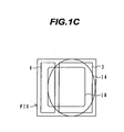
- Figs. 1A to 1C are a cross sectional view and plan views showing the outline structure of a solid state image pickup device according to an embodiment of the invention.
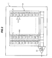
- Fig. 2 is a plan view showing the overall structure of a solid state image pickup device.
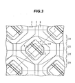
- Fig. 3 is a partial plan view showing the layout of a solid state image pickup device.
- Figs. 4A to 4E are cross sectional views and a plan view illustrating the function of the solid state image pickup device shown in Figs. 1A and 1B.
- Figs. 5A to 5D are cross sectional views illustrating the function of the solid state image pickup device shown in Fig. 1A and a schematic plan view illustrating shading prevention.
- Figs. 6A and 6B are cross sectional views illustrating the function of the solid state image pickup device shown in Fig. 1C.
- Figs. 7A to 7C are a schematic plan view showing a solid state image pickup device according to a second embodiment and cross sectional views illustrating the function of the solid image pickup device.
- Figs. 8A to 8C are schematic cross sectional views illustrating the function of the second embodiment.
- Figs. 9A to 9D are a schematic plan view showing a solid state image pickup device of the second embodiment and cross sectional views illustrating the function of the solid image pickup device.
- Figs. 10A and 10B are schematic plan views showing modifications of the first and second embodiments.
- Figs. 11A and 11B are a cross sectional view and a plan view illustrating prior art examples.
- Figs. 12A to 12C are a plan view and cross sectional views illustrating the outline of the contents of a previous application submitted by the present applicant.
- Fig. 1A is a schematic cross sectional view showing the structure of a solid state image pickup device according to a first embodiment of the invention.
- a p-type well 2 is formed in the surface layer of an n-type substrate 1.
- n-type regions 3 and 4 are formed in the surface layer of the p-type well 2.
- the p-type well 2 and n-type regions 3 and 4 constitute first and second photodiodes.
- a p-type element isolation region 5 is formed between the two n-type regions 3 and 4.
- Additionally formed in the surface layer of the p-type well 2 are VCCD n-channel regions 8, p-type element isolation regions 7, p+-type buried regions 6 and the like.
- Polysilicon transfer electrodes 10 and 11 are formed on an insulating layer 9 made of an oxide-nitride-oxide (ONO) film or the like formed on the semiconductor substrate surface.
- a light shielding film 12 of tungsten or the like is formed on an insulating layer covering the transfer electrodes 10 and 11.
- the light shielding film 12 has an opening 18 in an area corresponding to the central area of each pixel including a main photodiode 3 and a subsidiary photodiode 4.
- a partial area of the main photodiode 3 and a partial area of the subsidiary photodiode 4 are exposed in the opening to receive incidence light.
- An aperture ratio of the main photodiode 3 is set larger than that of the subsidiary photodiode 4. Therefore, the subsidiary photodiode has a lower sensitivity than that of the main photodiode, and the subsidiary photodiode is hard to be saturated.
- An insulating layer 13 made of a phosphorus glass layer or the like is formed on the light shielding film, the insulating layer having a planarized surface.
- Inner lenses 14 are formed on the planarized surface of the insulating layer 13. The optical axis of the inner lens 14 is shifted to the right of the center of the opening 18 of the light shielding film, i.e., toward the direction departing from the subsidiary photodiode area 4.
- the inner lens 14 is formed by depositing a silicon nitride film having a reflectivity of, for example, 1.8 to 2.4, forming a resist pattern on the silicon nitride film, softening and melting the resist pattern to form lens shapes, and thereafter transferring the lens shapes of the resist pattern to the silicon nitride film through anisotropical etching.
- a planarizing film 13a is formed burying the irregular surface of the inner lenses 14.
- the planarizing film 13a has a planarized surface and is made of an organic resin film, a phosphorus glass film, a boron-phosphorus glass film or the like.
- a color filter 15 is formed on the planarized surface.
- the color filter 15 includes color filters of three or more colors.
- a planarizing film 13b of an organic resin film or the like is formed burying the irregular surface of the color filter 15 and forming a planarized surface.
- On-chip micro lenses 16 are formed on the planarized surface of the planarizing film 13b.
- the on-chip micro lens 16 is formed by patterning a photoresist layer, softening and melting the patterned photoresist layer to form spherical surfaces, and thereafter curing the photoresist.
- the optical axis of the on-chip micro lens 16 is aligned approximately to the center of the opening 18 of the light shielding film 12. A light flux converged by the on-chip micro lens 16 propagates toward the opening 18.
- Fig. 1B is a schematic plan view showing the relation among the pixel PIX including the main photodiode 3 and subsidiary photodiode 4, the opening 18 of the light shielding film and the upper inner lens 14.
- the pixel FIX has a square quadrilateral shape.
- the rectangular main photodiode 3 and rectangular subsidiary photodiode 4 are juxtaposed occupying most of the area of the pixel PIX.
- the opening 18 is disposed in the central area of the pixel PIX.
- the main photodiode area 3 extends from the right end of the pixel to the left of the center of the opening 18. The center of the main photodiode is therefore at the right position of the center of the opening.
- the subsidiary photodiode area 4 extends from near the left end of the pixel, via the left end of the opening 18, partially into the opening area 18.
- the aperture ratio of the subsidiary photodiode 4, the ratio of the subsidiary photodiode area 4 to the area exposed to the opening 18, is set smaller than that of the main photodiode 3.
- An effective aperture ratio can be changed by converging incidence light with the on-chip micro lens and inner lens.
- the inner lens 14 is shifted to the right of the center of the opening 18 in such a manner that the focal point thereof is positioned in the main photodiode area 3. For example, if the left side of the main photodiode area 3 is spaced from the left side of the opening 18 by a distance d, the inner lens 14 is shifted by d/4 or more, e.g., d/2 or more and d or less from the center of the opening in the same direction.
- the on-chip micro lens 16 converges incidence light as much as possible toward the opening 18. Since the inner lens 14 is shifted toward the main photodiode area 3, a space is left on the side of the subsidiary photodiode 4. Therefore, the inner lens 14 receives most of the light converged by the on-chip micro lens 16, and further converges it to preferably focus it on the surface of the n-type region 3 of the semiconductor substrate. The effective aperture ratio can be increased further.
- Light converged by the on-chip micro lens 16 but not transmitted through the inner lens 14 passes through the opening 18 and becomes incident upon the surface of the subsidiary photodiode area 4. All of the light not passed through the inner lens 14 may not be incident upon the subsidiary photodiode area 4, but a portion thereof may be incident upon the main photodiode area 3 or upon the separation region 5 between the main and subsidiary photodiode. Since the light converged by the inner lens 14 becomes incident upon the main photodiode area 3, the main photodiode is set to a higher sensitivity and the subsidiary photodiode is set to a lower sensitivity (i.e., to a higher saturation light amount), than those corresponding to the actual aperture ratios.
- the plan shape of the inner lens 14 may be an elliptic shape having a short axis and a long axis in plane.
- Fig. 1A is a cross sectional view taken along the short axis direction of the elliptic inner lens 14.
- the elliptic inner lens 14 occupies a larger area of the main photodiode area 3, a space is left on the subsidiary photodiode 4 side. Therefore, the elliptic inner lens 14 receives most of the light converged by the on-chip micro lens 16, and further converges it to preferably focus it on the surface of the n-type region 3 of the semiconductor substrate along the short axis direction.
- the light is focused on a line along the extension direction of the main photodiode 3.
- the effective aperture ratio can be increased further by the divergence effect of the elliptic inner lens.
- Fig. 2 is a schematic plan view showing the overall structure of the semiconductor substrate of the solid state image pickup device having the pixel structure shown in Figs. 1A and 1B.
- a light reception area 20 is defined on the surface of the semiconductor chip 1, and a plurality of pixels PIXs are disposed in a matrix shape.
- Each pixel FIX includes a main photodiode 3 and a subsidiary photodiode 4.
- VCCD is disposed along each column of pixels PIXs.
- One HCCD 21 is disposed under a plurality of VCCDs.
- HCCD 21 transfers image signals of one row.
- An output circuit 22 is connected to an output end of HCCD 21.
- the layout of pixels is not limited to a square matrix.
- Fig. 3 shows an example of a honeycomb layout or pixel shift layout. Respective pixels each including the main and subsidiary photodiodes 3 and 4 are disposed shifted by a half pitch every row along the row direction. Therefore, respective pixels are also disposed shifted by a half pitch every column.
- a pixel is disposed in a space defined by these drive electrodes.
- a light shielding film above the transfer electrodes has an opening 18 in an area corresponding to the central area of each pixel.
- a partial area of the main photodiode area 3 and a partial area of the subsidiary photodiode area 4 are exposed in each opening 18.
- the aperture ratio of the main photodiode area 3 is set larger than that of the subsidiary photodiode area 4. Therefore, when light at the same intensity becomes incident, the main photodiode area 3 saturates first and then the subsidiary photodiode area 4 saturates.
- the sensitivity of the main photodiode is raised further so that the saturation light amount of the subsidiary photodiode becomes considerably larger than that of the main photodiode area 3.
- the main photodiode 3 In order not to lower the performance greatly as compared to that of one photodiode per pixel, it is desired to make the main photodiode 3 have an area as broad as possible to receive most of incidence light and provide a high sensitivity.
- the subsidiary photodiode area 4 is used so as to broaden the dynamic range at a high illuminance, and is used mainly for obtaining image information after the main photodiode area 3 is saturated.
- the subsidiary photodiode may have a lower precision than the main photodiode.
- the substrate surface area occupied by the subsidiary photodiode area 4 is set narrower than that of the main photodiode area so as not to lower the performance of the main photodiode.
- Fig. 4A light incident upon the semiconductor chip 1 of the solid state image pickup device has passed through a taking lens 30. Although generally perpendicular incidence light is received in the central area of the chip, the incidence light is slanted in the peripheral area of the chip.
- Fig. 4B the lateral direction along which the main photodiode area 3 and subsidiary photodiode area 4 are disposed in one pixel is represented by a direction X-X, and the direction perpendicular to the direction X-X is represented by a direction Y-Y.
- Fig. 4C is a cross section along the direction Y-Y when the incidence angle is 0 degree. Incidence light is focussed generally at the center of the main photodiode area 3.
- Fig. 4D shows the simulation result at the incidence angle of 7 degrees. As the incidence light is slanted by 7 degrees to the right direction, the focal position moves from the center to the left of the main photodiode area 3.
- Fig. 4E shows the simulation result at the incidence angle of - 7 degrees.
- the focal position moves from the center to the right of the main photodiode area 3. In either case, light is focussed in the central area of the main photodiode area 3 so that generally the uniform characteristics can be expected.
- Figs. 5A, 5B and 5C show the focussing states of light along the X-X direction.
- the subsidiary photodiode area 4 appears along with the main photodiode area 3. Changes in the focal position in the main photodiode area 3 are similar to those shown in Figs. 4C, 4D and 4E, and incidence light is focussed in the central area of the main photodiode area 3. In contrast, although there is incidence light at the incidence angles of 0 and - 7 degrees, there is no incidence light upon the subsidiary photodiode area 4.
- the light incidence angle is constant at each pixel.
- Fig. 5D is a schematic diagram illustrating a method of correcting the relation among the pixel, upper inner lens and upper on-chip micro lens to prevent shading.
- the positions of the on-chip micro lens, inner lens and pixel are shifted outward along the radial direction, the shift amount being increased in the order from the on-chip micro lens, inner lens and to the pixel and in the order from the light reception center to the outer periphery.
- Figs. 6A and 6B show the simulation results of light focussing states at the cross sections along the long and short axis directions of an elliptic inner lens such as shown in Fig. 1C.
- An elliptic inner lens has a short focal length in the short axis direction and a long focal length in the long axis direction.
- Fig. 6B shows the focussing state on a semiconductor substrate surface in the short axis direction. Since the focussing is made at one point, the position alignment margin for the focussing in the short side direction can be made large in the area of the rectangular main photodiode 3.
- Fig. 7A is a schematic plan view showing a pixel structure according to a second embodiment of the invention.
- a main photodiode area 3 is disposed in the central area of each pixel on the semiconductor substrate surface, and subsidiary photodiode areas 4 are disposed on both sides of the central area. It is preferable that the subsidiary photodiode areas are disposed symmetrical to the main photodiode area 3. With this layout, the subsidiary photodiode areas 4 on both sides of the central area operate complementarily.
- Fig. 7B shows a light propagation direction in the X-X cross section. Light passed through the inner lens becomes incident upon the main photodiode area 3, and outer light not passed through the inner lens becomes incident upon the subsidiary photodiode area 4.
- Fig. 7C shows the focussing state of light along the direction Y-Y.
- Light passed through the on-chip micro lens 16 and inner lens 14 focusses on the center of the main photodiode area 3. Outer light is focussed on the main photodiode area 3 although it does not pass through the inner lens 14.
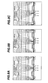
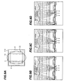
- Figs. 8A, 8B and 8C are cross sectional views showing the simulation results of a focussing state change with an incidence light angle along the direction of disposing the main and subsidiary photodiodes (direction X-X). The simulation results show the focussing state change at different incidence light angles.
- Figs. 8A, 8B and 8C show the focussing states at incidence light angles of 0, 7 and - 7 degrees, respectively.
- the incidence light angle is slanted, although one of the light fluxes outside the inner lens does not enter one subsidiary photodiode, the other enters the other subsidiary photodiode. It is therefore possible to avoid no incidence light upon the subsidiary photodiode.
- the slanted incidence light angle it is not easy to maintain constant an incidence light division ratio between the main and subsidiary photodiodes 3 and 4.
- the direction of incidence light upon each pixel is determined from the positional relation with the taking lens, and it is constant. Therefore, if two subsidiary photodiodes are used, a position shift for preventing shading may be performed in addition to the position shift for the case of a single subsidiary photodiode.
- Fig. 9A is a schematic plan view showing the pixel structure of the second embodiment using an elliptic inner lens such as shown in Fig. 1C.
- Fig. 9A corresponds to Fig. 7A.
- the cross sectional views shown in Figs. 9B, 9C and 9D correspond to those shown in Figs. 8A, 8B and 8C.
- Figs. 9B, 9C and 9D show the focusing states at incidence light angles of 0, 7 and - 7 degrees, respectively. Also in the case of the elliptic inner lens, as the incidence light angle is slanted, although one of the light fluxes outside the elliptic inner lens does not enter one subsidiary photodiode, the other enters the other subsidiary photodiode. It is therefore possible to avoid no incidence light upon the subsidiary photodiode. Shading can be prevented in the manner described earlier.
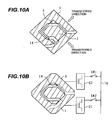
- Figs. 10A and 10B show modifications of the above-described embodiments.
- a subsidiary photodiode area 4 has a substantially symmetrical area surrounding a main photodiode area 3, and a connection area coupling these photodiode areas 3 and 4.
- the substantially symmetrical area implies the concept including the layout which provides a function equivalent to the symmetrical layout in terms of a photoelectric conversion function. Electric charges accumulated in the subsidiary photodiode area 4 are transferred to an upper right channel as shown in Fig. 10A, whereas electric charges accumulated in the main photodiode area 3 are transferred to an lower right channel.
- the subsidiary photodiode area 4 is exposed to incidence light only in the areas near the upper and lower corners of the an opening 18.
- Fig. 10B shows a MOS solid state image pickup device, not a CCD solid state image pickup device.
- MOS type charge detector circuits Q1 and Q2 are connected to a main photodiode area 3 and a subsidiary photodiode area 4 of each pixel. Outputs from the MOS type charge detector circuits Q1 and Q2 are supplied to output signal lines (image signal transfer units) TR via switches SW1 and SW2.
- the charge read mechanism is different, the function of receiving incidence light and photoelectrically converting it is similar to that of the embodiments described above.
- the solid state image pickup device of this invention is applicable to various apparatuses such as digital cameras and portable terminals, particularly to the apparatuses requiring a wide dynamic range.
Landscapes
- Solid State Image Pick-Up Elements (AREA)
- Transforming Light Signals Into Electric Signals (AREA)
Applications Claiming Priority (4)
| Application Number | Priority Date | Filing Date | Title |
|---|---|---|---|
| JP2003318356A JP4236169B2 (ja) | 2003-09-10 | 2003-09-10 | 固体撮像装置 |
| JP2003318355A JP4236168B2 (ja) | 2003-09-10 | 2003-09-10 | 固体撮像装置 |
| JP2003318355 | 2003-09-10 | ||
| JP2003318356 | 2003-09-10 |
Publications (2)
| Publication Number | Publication Date |
|---|---|
| EP1519416A2 true EP1519416A2 (de) | 2005-03-30 |
| EP1519416A3 EP1519416A3 (de) | 2008-08-06 |
Family
ID=34197196
Family Applications (1)
| Application Number | Title | Priority Date | Filing Date |
|---|---|---|---|
| EP04019747A Withdrawn EP1519416A3 (de) | 2003-09-10 | 2004-08-19 | Festkörperbildaufnahmevorrichtung |
Country Status (2)
| Country | Link |
|---|---|
| US (1) | US6903391B2 (de) |
| EP (1) | EP1519416A3 (de) |
Families Citing this family (30)
| Publication number | Priority date | Publication date | Assignee | Title |
|---|---|---|---|---|
| JP3709873B2 (ja) * | 2003-02-19 | 2005-10-26 | ソニー株式会社 | 固体撮像装置及び撮像カメラ |
| JP3885769B2 (ja) * | 2003-06-02 | 2007-02-28 | ソニー株式会社 | 固体撮像装置および固体撮像装置の駆動方法 |
| KR100562293B1 (ko) * | 2003-10-01 | 2006-03-22 | 동부아남반도체 주식회사 | 씨모스 이미지 센서 및 이의 제조 방법 |
| US7763918B1 (en) * | 2004-12-02 | 2010-07-27 | Chen Feng | Image pixel design to enhance the uniformity of intensity distribution on digital image sensors |
| US7450161B1 (en) | 2004-12-02 | 2008-11-11 | Magnachip Semiconductor Ltd. | System and method to enhance the uniformity of intensity distribution on digital imaging sensors |
| US7564629B1 (en) * | 2004-12-02 | 2009-07-21 | Crosstek Capital, LLC | Microlens alignment procedures in CMOS image sensor design |
| JP4840536B2 (ja) * | 2005-03-24 | 2011-12-21 | ソニー株式会社 | 固体撮像素子及び撮像装置 |
| JP4793042B2 (ja) * | 2005-03-24 | 2011-10-12 | ソニー株式会社 | 固体撮像素子及び撮像装置 |
| JP2006278620A (ja) * | 2005-03-29 | 2006-10-12 | Texas Instr Japan Ltd | 半導体装置およびその製造方法 |
| WO2007086352A1 (ja) * | 2006-01-25 | 2007-08-02 | Kyocera Corporation | 撮像素子及びカメラモジュール |
| JP2007208817A (ja) * | 2006-02-03 | 2007-08-16 | Toshiba Corp | 固体撮像装置 |
| US7638804B2 (en) * | 2006-03-20 | 2009-12-29 | Sony Corporation | Solid-state imaging device and imaging apparatus |
| JP5076679B2 (ja) * | 2007-06-28 | 2012-11-21 | ソニー株式会社 | 固体撮像装置及びカメラモジュール |
| CN101355659A (zh) * | 2007-07-27 | 2009-01-28 | 鸿富锦精密工业(深圳)有限公司 | 固态图像感测器 |
| EP2188838B1 (de) * | 2007-09-04 | 2015-04-01 | NDS Limited | Sicherheitschip |
| JP2009289927A (ja) * | 2008-05-28 | 2009-12-10 | Panasonic Corp | 固体撮像装置及びその製造方法 |
| US8350952B2 (en) * | 2008-06-04 | 2013-01-08 | Omnivision Technologies, Inc. | Image sensors with improved angle response |
| KR101776955B1 (ko) * | 2009-02-10 | 2017-09-08 | 소니 주식회사 | 고체 촬상 장치와 그 제조 방법, 및 전자 기기 |
| JP5556122B2 (ja) * | 2009-10-27 | 2014-07-23 | ソニー株式会社 | 固体撮像装置、固体撮像装置の製造方法、電子機器 |
| JP5091964B2 (ja) * | 2010-03-05 | 2012-12-05 | 株式会社東芝 | 固体撮像装置 |
| JP5741012B2 (ja) * | 2011-01-26 | 2015-07-01 | ソニー株式会社 | 固体撮像装置の製造方法 |
| US8742309B2 (en) | 2011-01-28 | 2014-06-03 | Aptina Imaging Corporation | Imagers with depth sensing capabilities |
| US10015471B2 (en) * | 2011-08-12 | 2018-07-03 | Semiconductor Components Industries, Llc | Asymmetric angular response pixels for single sensor stereo |
| WO2013051186A1 (ja) | 2011-10-03 | 2013-04-11 | パナソニック株式会社 | 撮像装置、撮像装置を用いたシステム及び測距装置 |
| US9554115B2 (en) * | 2012-02-27 | 2017-01-24 | Semiconductor Components Industries, Llc | Imaging pixels with depth sensing capabilities |
| JP6130221B2 (ja) * | 2013-05-24 | 2017-05-17 | ソニー株式会社 | 固体撮像装置、および電子機器 |
| KR102437162B1 (ko) | 2015-10-12 | 2022-08-29 | 삼성전자주식회사 | 이미지 센서 |
| WO2018069867A1 (en) * | 2016-10-13 | 2018-04-19 | Six Degrees Space Ltd | Method and apparatus for indoor positioning |
| KR102742271B1 (ko) * | 2019-11-15 | 2024-12-13 | 에스케이하이닉스 주식회사 | 이미지 센싱 장치 |
| CN111323978B (zh) * | 2020-04-08 | 2021-03-16 | Tcl华星光电技术有限公司 | 一种像素单元、阵列基板及显示面板 |
Citations (3)
| Publication number | Priority date | Publication date | Assignee | Title |
|---|---|---|---|---|
| JPH01140787A (ja) | 1987-11-27 | 1989-06-01 | Hitachi Ltd | 半導体レーザ素子 |
| US6259083B1 (en) | 1997-08-13 | 2001-07-10 | Sony Corporation | Solid state imaging device and manufacturing method thereof |
| US20020121652A1 (en) | 2000-11-28 | 2002-09-05 | Ryo Yamasaki | Image pickup apparatus |
Family Cites Families (10)
| Publication number | Priority date | Publication date | Assignee | Title |
|---|---|---|---|---|
| US4667092A (en) | 1982-12-28 | 1987-05-19 | Nec Corporation | Solid-state image device with resin lens and resin contact layer |
| JP2846928B2 (ja) | 1990-06-25 | 1999-01-13 | 北海製罐株式会社 | 缶蓋の巻締方法 |
| JPH09205589A (ja) | 1996-01-26 | 1997-08-05 | Sony Corp | 固体撮像装置 |
| JP3809708B2 (ja) | 1997-07-15 | 2006-08-16 | ソニー株式会社 | 固体撮像素子並びにその製造方法 |
| JP4092409B2 (ja) * | 1999-08-18 | 2008-05-28 | 富士フイルム株式会社 | 固体撮像素子 |
| JP4497688B2 (ja) * | 1999-09-27 | 2010-07-07 | 富士フイルム株式会社 | 固体撮像装置 |
| JP3928840B2 (ja) * | 2001-02-01 | 2007-06-13 | 富士フイルム株式会社 | 固体撮像装置 |
| JP4050906B2 (ja) | 2002-01-25 | 2008-02-20 | 富士フイルム株式会社 | 固体撮像装置 |
| JP4136611B2 (ja) * | 2002-11-07 | 2008-08-20 | 富士フイルム株式会社 | 固体撮像素子 |
| EP1557886A3 (de) * | 2004-01-26 | 2006-06-07 | Matsushita Electric Industrial Co., Ltd. | Festkörperbildaufnahmevorrichtung und Kamera |
-
2004
- 2004-05-24 US US10/851,416 patent/US6903391B2/en not_active Expired - Fee Related
- 2004-08-19 EP EP04019747A patent/EP1519416A3/de not_active Withdrawn
Patent Citations (3)
| Publication number | Priority date | Publication date | Assignee | Title |
|---|---|---|---|---|
| JPH01140787A (ja) | 1987-11-27 | 1989-06-01 | Hitachi Ltd | 半導体レーザ素子 |
| US6259083B1 (en) | 1997-08-13 | 2001-07-10 | Sony Corporation | Solid state imaging device and manufacturing method thereof |
| US20020121652A1 (en) | 2000-11-28 | 2002-09-05 | Ryo Yamasaki | Image pickup apparatus |
Also Published As
| Publication number | Publication date |
|---|---|
| EP1519416A3 (de) | 2008-08-06 |
| US20050051860A1 (en) | 2005-03-10 |
| US6903391B2 (en) | 2005-06-07 |
Similar Documents
| Publication | Publication Date | Title |
|---|---|---|
| US6903391B2 (en) | Solid state image pickup device | |
| KR101036290B1 (ko) | 고체촬상장치 및 그 제조방법 | |
| EP0948055B1 (de) | Festkörper-Bildaufnahmevorrichtung | |
| KR100654146B1 (ko) | 고체 촬상 장치 및 카메라 | |
| CN118866922A (zh) | 光检测装置和电子设备 | |
| EP1331670B1 (de) | Festkörper-Bildaufnahmevorrichtung mit zwei photoempfindlichen Bereichen pro Pixel | |
| CN100580941C (zh) | 半导体成像器件 | |
| JP2003338615A (ja) | 固体撮像装置 | |
| JP4236169B2 (ja) | 固体撮像装置 | |
| CN101425527A (zh) | 固态成像装置、其制造和驱动方法和照相机 | |
| JP2015142114A (ja) | 固体撮像装置 | |
| US8773559B2 (en) | Solid-state imaging device and method of manufacturing the same, and imaging apparatus | |
| JP4682504B2 (ja) | 固体撮像装置及びその製造方法並びに電子機器 | |
| JP2007067379A (ja) | 固体撮像装置 | |
| JP3684169B2 (ja) | 固体撮像装置 | |
| JP4236168B2 (ja) | 固体撮像装置 | |
| JP2024072796A (ja) | イメージセンサ及びその製造方法 | |
| JP2866328B2 (ja) | 固体撮像素子 | |
| US7719040B2 (en) | Solid-state imaging device | |
| KR20060054147A (ko) | 촬상 소자 | |
| JP2003078125A (ja) | 固体撮像装置 | |
| JP4216935B2 (ja) | 半導体装置の製造方法 | |
| KR20010106831A (ko) | 전자 줌 기능에 적합한 고체 촬상 소자 | |
| JP2007158312A (ja) | 固体撮像素子 | |
| KR100262035B1 (ko) | 고체촬상소자의 제조방법 |
Legal Events
| Date | Code | Title | Description |
|---|---|---|---|
| PUAI | Public reference made under article 153(3) epc to a published international application that has entered the european phase |
Free format text: ORIGINAL CODE: 0009012 |
|
| AK | Designated contracting states |
Kind code of ref document: A2 Designated state(s): AT BE BG CH CY CZ DE DK EE ES FI FR GB GR HU IE IT LI LU MC NL PL PT RO SE SI SK TR |
|
| AX | Request for extension of the european patent |
Extension state: AL HR LT LV MK |
|
| RAP1 | Party data changed (applicant data changed or rights of an application transferred) |
Owner name: FUJIFILM CORPORATION |
|
| PUAL | Search report despatched |
Free format text: ORIGINAL CODE: 0009013 |
|
| AK | Designated contracting states |
Kind code of ref document: A3 Designated state(s): AT BE BG CH CY CZ DE DK EE ES FI FR GB GR HU IE IT LI LU MC NL PL PT RO SE SI SK TR |
|
| AX | Request for extension of the european patent |
Extension state: AL HR LT LV MK |
|
| RIC1 | Information provided on ipc code assigned before grant |
Ipc: H01L 27/148 20060101ALI20080630BHEP Ipc: H01L 27/146 20060101AFI20050204BHEP |
|
| 17P | Request for examination filed |
Effective date: 20080915 |
|
| AKX | Designation fees paid |
Designated state(s): DE FR GB |
|
| 17Q | First examination report despatched |
Effective date: 20101007 |
|
| STAA | Information on the status of an ep patent application or granted ep patent |
Free format text: STATUS: THE APPLICATION IS DEEMED TO BE WITHDRAWN |
|
| 18D | Application deemed to be withdrawn |
Effective date: 20111222 |