EP1518145B1 - Anzeigezelle, insbesondere flüssigkristall- oder photovoltaische zelle mit mitteln zur verbindung mit einer elektronischen steuerschaltung - Google Patents
Anzeigezelle, insbesondere flüssigkristall- oder photovoltaische zelle mit mitteln zur verbindung mit einer elektronischen steuerschaltung Download PDFInfo
- Publication number
- EP1518145B1 EP1518145B1 EP03740263A EP03740263A EP1518145B1 EP 1518145 B1 EP1518145 B1 EP 1518145B1 EP 03740263 A EP03740263 A EP 03740263A EP 03740263 A EP03740263 A EP 03740263A EP 1518145 B1 EP1518145 B1 EP 1518145B1
- Authority
- EP
- European Patent Office
- Prior art keywords
- cell
- substrates
- cell according
- conductive
- electrodes
- Prior art date
- Legal status (The legal status is an assumption and is not a legal conclusion. Google has not performed a legal analysis and makes no representation as to the accuracy of the status listed.)
- Expired - Lifetime
Links
- 239000004973 liquid crystal related substance Substances 0.000 title claims abstract description 35
- 210000004027 cell Anatomy 0.000 claims abstract description 143
- 239000000758 substrate Substances 0.000 claims abstract description 49
- 239000004020 conductor Substances 0.000 claims abstract description 16
- 238000007789 sealing Methods 0.000 claims abstract description 13
- 210000002858 crystal cell Anatomy 0.000 claims description 17
- 230000002745 absorbent Effects 0.000 claims description 4
- 239000002250 absorbent Substances 0.000 claims description 4
- 238000005304 joining Methods 0.000 claims description 3
- 230000000930 thermomechanical effect Effects 0.000 claims description 2
- 230000002040 relaxant effect Effects 0.000 claims 1
- 239000000126 substance Substances 0.000 claims 1
- PEDCQBHIVMGVHV-UHFFFAOYSA-N Glycerine Chemical compound OCC(O)CO PEDCQBHIVMGVHV-UHFFFAOYSA-N 0.000 description 20
- 238000004519 manufacturing process Methods 0.000 description 10
- 238000000034 method Methods 0.000 description 8
- 230000035882 stress Effects 0.000 description 5
- 230000000694 effects Effects 0.000 description 4
- 238000000151 deposition Methods 0.000 description 3
- 238000005530 etching Methods 0.000 description 3
- 239000011521 glass Substances 0.000 description 3
- 239000002184 metal Substances 0.000 description 3
- 230000003287 optical effect Effects 0.000 description 3
- 230000001154 acute effect Effects 0.000 description 2
- 230000008859 change Effects 0.000 description 2
- 230000007423 decrease Effects 0.000 description 2
- 230000008021 deposition Effects 0.000 description 2
- 238000000608 laser ablation Methods 0.000 description 2
- 239000007788 liquid Substances 0.000 description 2
- 239000000463 material Substances 0.000 description 2
- 238000001465 metallisation Methods 0.000 description 2
- 230000000704 physical effect Effects 0.000 description 2
- 230000005855 radiation Effects 0.000 description 2
- 238000002310 reflectometry Methods 0.000 description 2
- 239000012780 transparent material Substances 0.000 description 2
- 241001639412 Verres Species 0.000 description 1
- 239000006096 absorbing agent Substances 0.000 description 1
- 239000013078 crystal Substances 0.000 description 1
- 230000005611 electricity Effects 0.000 description 1
- 230000008020 evaporation Effects 0.000 description 1
- 238000001704 evaporation Methods 0.000 description 1
- 230000002349 favourable effect Effects 0.000 description 1
- 239000012530 fluid Substances 0.000 description 1
- 239000003292 glue Substances 0.000 description 1
- 239000011159 matrix material Substances 0.000 description 1
- 229910001092 metal group alloy Inorganic materials 0.000 description 1
- 238000012986 modification Methods 0.000 description 1
- 230000004048 modification Effects 0.000 description 1
- 230000002093 peripheral effect Effects 0.000 description 1
- 238000000206 photolithography Methods 0.000 description 1
- 229920003223 poly(pyromellitimide-1,4-diphenyl ether) Polymers 0.000 description 1
- 230000008569 process Effects 0.000 description 1
- 238000011084 recovery Methods 0.000 description 1
- 230000008646 thermal stress Effects 0.000 description 1
Images
Classifications
-
- G—PHYSICS
- G02—OPTICS
- G02F—OPTICAL DEVICES OR ARRANGEMENTS FOR THE CONTROL OF LIGHT BY MODIFICATION OF THE OPTICAL PROPERTIES OF THE MEDIA OF THE ELEMENTS INVOLVED THEREIN; NON-LINEAR OPTICS; FREQUENCY-CHANGING OF LIGHT; OPTICAL LOGIC ELEMENTS; OPTICAL ANALOGUE/DIGITAL CONVERTERS
- G02F1/00—Devices or arrangements for the control of the intensity, colour, phase, polarisation or direction of light arriving from an independent light source, e.g. switching, gating or modulating; Non-linear optics
- G02F1/01—Devices or arrangements for the control of the intensity, colour, phase, polarisation or direction of light arriving from an independent light source, e.g. switching, gating or modulating; Non-linear optics for the control of the intensity, phase, polarisation or colour
- G02F1/13—Devices or arrangements for the control of the intensity, colour, phase, polarisation or direction of light arriving from an independent light source, e.g. switching, gating or modulating; Non-linear optics for the control of the intensity, phase, polarisation or colour based on liquid crystals, e.g. single liquid crystal display cells
- G02F1/133—Constructional arrangements; Operation of liquid crystal cells; Circuit arrangements
- G02F1/1333—Constructional arrangements; Manufacturing methods
- G02F1/1345—Conductors connecting electrodes to cell terminals
-
- C—CHEMISTRY; METALLURGY
- C23—COATING METALLIC MATERIAL; COATING MATERIAL WITH METALLIC MATERIAL; CHEMICAL SURFACE TREATMENT; DIFFUSION TREATMENT OF METALLIC MATERIAL; COATING BY VACUUM EVAPORATION, BY SPUTTERING, BY ION IMPLANTATION OR BY CHEMICAL VAPOUR DEPOSITION, IN GENERAL; INHIBITING CORROSION OF METALLIC MATERIAL OR INCRUSTATION IN GENERAL
- C23C—COATING METALLIC MATERIAL; COATING MATERIAL WITH METALLIC MATERIAL; SURFACE TREATMENT OF METALLIC MATERIAL BY DIFFUSION INTO THE SURFACE, BY CHEMICAL CONVERSION OR SUBSTITUTION; COATING BY VACUUM EVAPORATION, BY SPUTTERING, BY ION IMPLANTATION OR BY CHEMICAL VAPOUR DEPOSITION, IN GENERAL
- C23C14/00—Coating by vacuum evaporation, by sputtering or by ion implantation of the coating forming material
- C23C14/22—Coating by vacuum evaporation, by sputtering or by ion implantation of the coating forming material characterised by the process of coating
- C23C14/225—Oblique incidence of vaporised material on substrate
-
- G—PHYSICS
- G02—OPTICS
- G02F—OPTICAL DEVICES OR ARRANGEMENTS FOR THE CONTROL OF LIGHT BY MODIFICATION OF THE OPTICAL PROPERTIES OF THE MEDIA OF THE ELEMENTS INVOLVED THEREIN; NON-LINEAR OPTICS; FREQUENCY-CHANGING OF LIGHT; OPTICAL LOGIC ELEMENTS; OPTICAL ANALOGUE/DIGITAL CONVERTERS
- G02F1/00—Devices or arrangements for the control of the intensity, colour, phase, polarisation or direction of light arriving from an independent light source, e.g. switching, gating or modulating; Non-linear optics
- G02F1/01—Devices or arrangements for the control of the intensity, colour, phase, polarisation or direction of light arriving from an independent light source, e.g. switching, gating or modulating; Non-linear optics for the control of the intensity, phase, polarisation or colour
- G02F1/13—Devices or arrangements for the control of the intensity, colour, phase, polarisation or direction of light arriving from an independent light source, e.g. switching, gating or modulating; Non-linear optics for the control of the intensity, phase, polarisation or colour based on liquid crystals, e.g. single liquid crystal display cells
- G02F1/133—Constructional arrangements; Operation of liquid crystal cells; Circuit arrangements
- G02F1/1333—Constructional arrangements; Manufacturing methods
- G02F1/1345—Conductors connecting electrodes to cell terminals
- G02F1/13452—Conductors connecting driver circuitry and terminals of panels
-
- H—ELECTRICITY
- H05—ELECTRIC TECHNIQUES NOT OTHERWISE PROVIDED FOR
- H05K—PRINTED CIRCUITS; CASINGS OR CONSTRUCTIONAL DETAILS OF ELECTRIC APPARATUS; MANUFACTURE OF ASSEMBLAGES OF ELECTRICAL COMPONENTS
- H05K3/00—Apparatus or processes for manufacturing printed circuits
- H05K3/10—Apparatus or processes for manufacturing printed circuits in which conductive material is applied to the insulating support in such a manner as to form the desired conductive pattern
- H05K3/14—Apparatus or processes for manufacturing printed circuits in which conductive material is applied to the insulating support in such a manner as to form the desired conductive pattern using spraying techniques to apply the conductive material, e.g. vapour evaporation
- H05K3/146—By vapour deposition
-
- H—ELECTRICITY
- H05—ELECTRIC TECHNIQUES NOT OTHERWISE PROVIDED FOR
- H05K—PRINTED CIRCUITS; CASINGS OR CONSTRUCTIONAL DETAILS OF ELECTRIC APPARATUS; MANUFACTURE OF ASSEMBLAGES OF ELECTRICAL COMPONENTS
- H05K3/00—Apparatus or processes for manufacturing printed circuits
- H05K3/40—Forming printed elements for providing electric connections to or between printed circuits
- H05K3/403—Edge contacts; Windows or holes in the substrate having plural connections on the walls thereof
Definitions
- the present invention relates to a device defining a volume for the confinement of a fluid such as a liquid crystal and, more generally, a material susceptible to change physical properties, including optical, under the effect of the application of a voltage, or electrical properties under the effect of a stress or radiation.
- a display device comprising means for connection to a circuit electronic control.
- a liquid crystal cell is composed of essentially a transparent front substrate and a back substrate also transparent or not, these two substrates being united and kept at a distance constant one of the other by a sealing frame which delimits a sealed volume for the confinement of the liquid crystal.
- the substrates front and back each comprise, on their facing faces, at least one electrode, these electrodes being intended to be connected to an electronic control circuit which, by selective application of appropriate voltages to specific electrodes, allows to modify the optical properties of the liquid crystal at the point of intersection of electrodes considered.
- a constant problem in the field of manufacturing crystal cells liquids of the type described above is set by the connecting means for establish the electrical connection between the electrodes of the cell and the control circuit.
- a simple technique for making the electrical connection between the electrodes and the control circuit is to shift the substrates relative to each other, if although one can access a flat part of the electrodes and easily realize the connection on the surface thus cleared.
- Such an arrangement of substrates makes however the manufacture of cells in series difficult, especially when they are circular, and require additional time-consuming operations.
- the resulting cells are, in addition, larger and therefore difficult to housed in small portable electronic objects such as a wristwatch.
- an electro-optical cell such as a liquid crystal cell, or an electrochemical photovoltaic cell, these cells each consisting of a transparent front substrate, a rear substrate also transparent or not, a sealing frame joining the two substrates and defining a volume for the sealed confinement of a photoelectric medium or electro-optically active, the substrates having on their faces opposite the least one electrode.
- electro-optical cell such as a liquid crystal cell, or an electrochemical photovoltaic cell
- these cells each consisting of a transparent front substrate, a rear substrate also transparent or not, a sealing frame joining the two substrates and defining a volume for the sealed confinement of a photoelectric medium or electro-optically active, the substrates having on their faces opposite the least one electrode.
- These cells are distinguished by the fact that their electrodes are partially flush with the edge of the substrate on which they are deposited to define lateral electrical contact zones at which they are reported angle pieces which advantageously allow to postpone the electrical contact on the rear face of said cells.
- JP 56 075624 is known and JP 56 168628 on which the preamble of the first claim is based, and both of which describe liquid crystal cells on the wafer and the rear face of which conductive tracks are deposited by printing.
- display cell substrates can be of substantially equal size and no longer need to be shifted one by to each other to allow for the establishment of electrical connections between electrodes and the control circuit.
- the active surface of a liquid crystal cell can be increased, one can increase the resolution of the display, that is to say predict a larger number electrodes of lines and columns, without opening or opening pixels, and so the reflectivity of the display cell, are altered.
- the means for connect the electrodes of a display cell to a control circuit are not formed by contact pieces that would need to be glued one by one, but conductive tracks which allow to postpone the electrical contacts formed by the electrodes of a cell from the edge of the cell to the back edge of said cell, then from there around said rear edge and up to the back of the cell, these conductive tracks being formed on the edge and the back of the cell by any appropriate technique for the deposition and etching of conductive layers to achieve the desired dimensions and resolution.
- the conductive tracks which are in the form of thin layers, have problems of reliability and continuity electrical conduction where they marry the back edge, often acute, of the cell. Indeed, the thermal stresses that appear during the cell manufacturing process can cause tearing of the tracks conductors at the edge of the rear substrate of the cell. Likewise, a thin layer deposited around the rear edge of the cell has a low holding mechanical and can be easily scratched and interrupted when manipulating the cell or want to mount it in the portable object for which it is intended.
- the present invention aims to remedy the aforementioned problems as well as others by providing a display device, including crystal liquid, comprising means for connecting its electrodes to a circuit control electronics that are both simple to manufacture and reliable.
- these contact means are in the form of discrete studs.
- conductive pads are arranged on at at least a portion of the rear periphery of the cell, so as to replace the arrangement conductive tracks around the rear edge of the cell by making contact side on the opposite faces of the conductive pads much more reliable and more mechanically resistant.
- the present invention relates to a cell comprising a stack of (n) individual cells (where n is a number natural number greater than or equal to 2), each of the individual cells being delimited by two substrates of its own, or a cell comprising (n + 1) superimposed substrates (where n is an integer greater than or equal to 1), these (n + 1) substrates being joined two by two by a sealing frame.
- the present invention will be described in connection with a display cell to liquid crystal. It goes without saying that the present invention is not limited to such a type of cell, and that it can be applied to any type of cell comprising a medium susceptible to change physical properties, including optical, under the effect of the application of a voltage, or electrical properties under the effect of a stress or radiation.
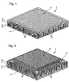
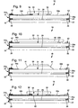
- FIGS 1 and 2 are perspective views respectively at the location and backside of an unclaimed multilayer LCD display cell.
- this cell display includes four superposed substrates 2, 4, 6 and 8 which can be made of glass or other transparent material such as plastic.
- the last substrate 8 may be transparent or not depending on the reflective nature or transmissive of the display cell 1.
- the rear substrate 8 may be opaque or covered with a layer of opacifying material in order to mask the integrated circuit 10 in the view of an observer located on the front side 14 of the cell 1.
- Substrates 2 to 8 are joined in pairs by sealing frames (no visible in Figures 1 and 2) which each delimit a sealed cavity for the confinement of the liquid crystals. More specifically, a first sealing frame substrates 2 and 4, while a second sealing frame brings together the substrates 4 and 6 and that a third and final sealing frame joins the substrates 6 and 8.
- the electrodes of the cell 1 are flush with the slice 15 of the cell 1 in separate areas of its perimeter to define areas of electrical contact side.
- Conductive tracks 16 which come into contact with the electrodes at level of the lateral electrical contact zones are formed directly on the slice 15 and the back 12 of cell 1, so as to postpone all contacts in the same rear plane of said cell 1.
- Conductive tracks 16 therefore extend from the electrodes of cell 1 to the input ports of the circuit integrated control 10 of the display which is mounted on the back 12 of the cell 1 by techniques that will be described in detail later.
- FIGS. 1 and 2 sees that the conductive tracks are not of equal length and stop just where the electrodes are flush with the edge of the cell. It is obvious that the conductive tracks have been so represented to better understand the way the electrical connections are established between the electrodes and the said conductive tracks but, in practice, we prefer to make tracks conductors of identical lengths.
- this surface device that is normally assigned to the connection of the cell and which, proportionately, impinges even more on the active surface of the cell than this last is small, can be deleted. This is particularly advantageous when, for the same active surface of the cell, the number of row electrodes and columns increases. Indeed, in this case, the width of the electrodes decreases, and to keep the surface of the electrical contact areas constant, lengthening the electrodes, which would increase the non-active area around of the display cell.
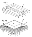
- FIG. 3 is a schematic view in perspective and in transparency of a unclaimed liquid crystal cell 18 comprising two substrates 20 and 22 which may be made of glass or other transparent material such as plastic.
- the substrates 20 and 22 are joined together by a sealing frame which delimits a sealed volume for the confinement of the liquid crystals.
- Only two electrodes 24 and 26 have been shown in the drawing. It goes without saying, however, that in reality the cell 18 comprises a multiplicity of electrodes which are formed on the faces in substrates 20 and 22.
- the electrode 24 extends over substantially the total length of the substrate 20 on which it was deposited and comes, at one of its ends, flush with the wafer 27 of said substrate 20 to define a zone 28 of lateral electrical contact.
- a conductive track 30 which is formed on the slice 27 and the back 31 of the cell 18 comes into contact with the electrode 24 at the of the contact zone 28, so as to postpone the electrical contact in the rear plane of said cell 18.
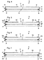
- Figure 4 is a longitudinal sectional view of the liquid crystal cell 18 unclaimed represented in Figure 3.
- the frame of seal 36 which defines the volume 38 for the confinement of the liquid crystal.
- the electrodes 24 and 26 pass under the sealing frame 36 and come flush with the slice 27 of the substrate 20 on which they were formed to define the zones of lateral electrical contact respectively 28 and 32.
- the conductive tracks 30 and 34 allow to postpone the electrical contacts formed by the electrodes 24 and 26 of the liquid crystal cell 18 from the slice 27 of the cell 18 to the edge or rear edge 40 of said cell, then from there around said rear edge 40 and up to the back 31 of the cell 18.
- the conductive tracks 30 and 34 are formed by deposition of thin layers of an electrically conductive material as will be described in detail later. It can therefore be feared that the conductive tracks have problems with resistance to heat and mechanical stress and tear where they marry the rear edge 40, often acute, of the cell, during the manufacture of the cell or when handling it. That is why, according to the embodiment illustrated in Figures 5 and 6, is formed along the rear edge 40 of the cell conductive pads 42 to ensure the continuity of the tracks conductors 30 and 34.
- the conductive tracks 30 and 34 each consist of a first part, respectively 30a and 34a, which extends on at least a portion of the slice 27 of the cell 18, and a second portion, respectively 30b and 34b, which extends over at least a portion of the back 31 of the cell 18, the conductive pads 42 ensuring the electrical connection between the first and the second portions of said conductive tracks 30 and 34. More specifically, the first portions 30a and 34a of the conductive tracks 30 and 34 come laterally in contact with the conductive pads 42, while the second parts 30b and 34b said conductive tracks 30 and 34 may extend to the top of said pads 42 and even partially cover them. In this way, we replace the arrangement of conductive tracks 30, 34 around the rear edge 40 of the cell 18 by taking a lateral contact on the opposite faces 44 and 46 of the conductive pads 42.
- parts 30b and 34b of the conductive tracks 30 and 34 extend at least partially under the conducting studs 42.
- At least some of the pads 42 may be provided on the edge 27 of the cell 18.
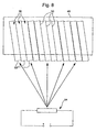
- a thin layer of conductive material is evaporated on the back of cells while they are still in batch or batch. After individualization of the cells, a group of them is arranged in a support or posage 48 (see Figure 8). The cells are arranged parallel to each other in oblique and slightly offset from each other, so that their long sides 50 are parallel and their little sides 52 that are meant to be metallized are arranged in a staggered manner.
- a source of evaporation 54 an electrically conductive material is disposed facing the facing 48, facing at the slices 52 of the cells to be metallized.
- the conductive tracks After metallization of the back 31 and the slice 27 of the cells, it is necessary to structure the conductive tracks, for example by laser ablation. For the sake of economy and to obtain a better performance, only the first parts 30a, 34a tracks conductive 30, 34 which extend on the edge 27 of the liquid crystal cells 18 will be structured by laser ablation, while the second parts 30b, 34b of these same conductive tracks 30, 34 which extend to the back 31 of the cells 18 may be structured by conventional photolithography techniques.
- FIG. 9 in which an integrated circuit is shown 56 control of the display is mounted directly on the back 31 of the cell 18.
- the integrated circuit 56 is mounted returned to the display cell 18, better known technique under its name Anglo-Saxon "flip chip bonding", so that its input ports 58 are pasted on the conductive tracks 30, 34 of the cell 18.
- the input ports 58 of the integrated circuit 56 could be connected to the tracks conductors 30, 34 by fine conductive wires, a technique better known in its Anglo-Saxon denomination "wire bonding".
- integrated control circuit 56 is mounted on the back 31 of the display cell to liquid crystal 18 not directly but through a circuit board printed 60.
- the integrated control circuit 56 is mounted on the back 31 of the cell liquid crystal display 18 via a flexible conductive film 61 made in Kapton®, a technique better known by its Anglo-Saxon name “Tape automatic bonding” or TAB.
- the absorbent layer It will also be necessary for the absorbent layer to be able to withstand etching baths when etching the metal layer on the back of the cell.
Landscapes
- Physics & Mathematics (AREA)
- Chemical & Material Sciences (AREA)
- Nonlinear Science (AREA)
- Crystallography & Structural Chemistry (AREA)
- General Physics & Mathematics (AREA)
- Optics & Photonics (AREA)
- Mathematical Physics (AREA)
- Engineering & Computer Science (AREA)
- Chemical Kinetics & Catalysis (AREA)
- Materials Engineering (AREA)
- Mechanical Engineering (AREA)
- Metallurgy (AREA)
- Organic Chemistry (AREA)
- Liquid Crystal (AREA)
- Devices For Indicating Variable Information By Combining Individual Elements (AREA)
- Credit Cards Or The Like (AREA)
- Combinations Of Printed Boards (AREA)
- Electric Clocks (AREA)
- Photovoltaic Devices (AREA)
Claims (11)
- Elektrooptische Anzeigezelle (1; 18), insbesondere mit Flüssigkristallen, oder elektrochemische photovoltaische Zelle, die umfasst:wobei diese Zelle dadurch gekennzeichnet ist, dass die Leiterbahnen (30, 34) jeweils aus einem ersten Teil (30a, 34a), der mit den Elektroden auf Höhe der seitlichen elektrischen Kontaktzonen (28, 32) in Kontakt ist, und aus einem zweiten Teil (30b, 34b), der sich auf der hinteren Oberfläche (31) der Zelle (18) erstreckt, aufgebaut sind, wobei Kontaktmittel (42), die kontinuierlich oder diskontinuierlich wenigstens längs eines Teils des unteren Umfangs (40) der Zelle (1; 18) auf der Schnittfläche (27) und/oder auf der hinteren Fläche (12; 31) der Zelle (1; 18) vorgesehen sind, die elektrische Verbindung zwischen den ersten Teilen (30a, 34a) und den zweiten Teilen (30b, 34b) der Leiterbahnen (30, 34) sicherstellen.wenigstens ein lichtdurchlässiges vorderes Substrat (2; 22), dessen obere Oberfläche die vordere Fläche (14) der Zelle (1; 18) bildet;wenigstens ein hinteres Substrat (8; 22), das ebenfalls lichtdurchlässig oder nicht lichtdurchlässig sein kann, dessen untere Oberfläche (12; 31) die hintere Fläche der Zelle (1; 18) bildet;einen Einkapselungsrahmen (36), der das vordere Substrat (2; 22) und das hintere Substrat (8; 20) miteinander vereinigt und ein Volumen (38) für die dichte Einkapselung eines elektrooptisch oder photoelektrisch aktiven Milieus begrenzt;wobei das vordere Substrat (2; 22) und das hintere Substrat (8; 20) auf ihren einander zugewandten Flächen wenigstens jeweils eine Elektrode (24, 26) aufweisen, wobei diese Elektroden (24, 26) mit Leiterbahnen (16; 30, 34) verbunden sind, die ihrerseits dazu vorgesehen sind, mit einer elektrischen Versorgungs- oder Steuerschaltung (10; 56) verbunden zu werden, und Zonen (28, 32) für einen seitlichen elektrischen Kontakt an den Stellen, an denen sie mit der Schnittfläche der Zelle bündig sind, definieren,
- Zelle nach Anspruch 1, dadurch gekennzeichnet, dass die Kontaktmittel (42) die Form diskreter Anschlussflächen besitzen.
- Zelle nach Anspruch 2, dadurch gekennzeichnet, dass die ersten Teile (30a, 34a) der Leiterbahnen (30, 34) seitlich mit den Leiter-Anschlussflächen (42) in Kontakt gelangen, während die zweiten Teile (30b, 34b) der Leiterbahnen (30, 34) sich bis zur Spitze der Anschlussflächen (42) erstrecken und sie ganz oder teilweise abdecken.
- Zelle nach Anspruch 2, dadurch gekennzeichnet, dass sich die zweiten Teile (30b, 34b) der Leiterbahnen wenigstens teilweise unter den Leiter-Anschlussflächen (42) erstrecken.
- Zelle nach Anspruch 1, dadurch gekennzeichnet, dass die Kontaktmittel (42) die Form eines Streifens (64) aus einem anisotropen leitenden Material haben.
- Zelle nach einem der Ansprüche 1 bis 5, dadurch gekennzeichnet, dass sie einen Stapel aus (n) einzelnen Zellen umfasst, wovon jede durch zwei Substrate begrenzt ist, die ihr gemeinsam sind.
- Zelle nach einem der Ansprüche 1 bis 5, dadurch gekennzeichnet, dass sie (n + 1) übereinander liegende Substrate umfasst, die paarweise durch einen Einkapselungsrahmen miteinander vereinigt sind.
- Zelle nach einem der Ansprüche 1 bis 7, dadurch gekennzeichnet, dass die Versorgungs- oder Steuerschaltung (10; 56) auf der hinteren Fläche (12; 31) der Zelle (1; 18) montiert ist.
- Zelle nach Anspruch 8, dadurch gekennzeichnet, dass die Schaltung (10; 56) direkt auf der hinteren Fläche (12; 31) der Zelle (1; 18) montiert ist.
- Zelle nach Anspruch 8, dadurch gekennzeichnet, dass die Schaltung (10; 56) über eine gedruckte Leiterplatte (60) oder eine biegsame Leiterschicht (61) auf der hinteren Fläche (12; 31) der Zelle (1; 18) montiert ist.
- Zelle nach einem der Ansprüche 1 bis 10, dadurch gekennzeichnet, dass auf der hinteren Fläche der Zelle (18) eine lichtdurchlässige oder gefärbte Absorptionsschicht (62) aufgebracht ist, die eine Lösung thermomechanischer Spannungen ermöglicht und einem chemischen Angriffsbad widerstehen kann.
Priority Applications (1)
| Application Number | Priority Date | Filing Date | Title |
|---|---|---|---|
| EP03740263A EP1518145B1 (de) | 2002-06-21 | 2003-06-17 | Anzeigezelle, insbesondere flüssigkristall- oder photovoltaische zelle mit mitteln zur verbindung mit einer elektronischen steuerschaltung |
Applications Claiming Priority (4)
| Application Number | Priority Date | Filing Date | Title |
|---|---|---|---|
| EP02077490A EP1376212A1 (de) | 2002-06-21 | 2002-06-21 | Anzeigezelle, insbesondere eine Flüssigkristallzelle, oder Photovoltaikzelle mit Verbindungsmitteln zu einem Treiberschaltkreis |
| EP02077490 | 2002-06-21 | ||
| EP03740263A EP1518145B1 (de) | 2002-06-21 | 2003-06-17 | Anzeigezelle, insbesondere flüssigkristall- oder photovoltaische zelle mit mitteln zur verbindung mit einer elektronischen steuerschaltung |
| PCT/EP2003/006376 WO2004001495A2 (fr) | 2002-06-21 | 2003-06-17 | Cellule d'affichage, notamment a cristal liquide, ou cellule photovoltaique comprenant des moyens pour sa connexion a un circuit electronique de commande |
Publications (2)
| Publication Number | Publication Date |
|---|---|
| EP1518145A2 EP1518145A2 (de) | 2005-03-30 |
| EP1518145B1 true EP1518145B1 (de) | 2005-12-14 |
Family
ID=29716891
Family Applications (2)
| Application Number | Title | Priority Date | Filing Date |
|---|---|---|---|
| EP02077490A Withdrawn EP1376212A1 (de) | 2002-06-21 | 2002-06-21 | Anzeigezelle, insbesondere eine Flüssigkristallzelle, oder Photovoltaikzelle mit Verbindungsmitteln zu einem Treiberschaltkreis |
| EP03740263A Expired - Lifetime EP1518145B1 (de) | 2002-06-21 | 2003-06-17 | Anzeigezelle, insbesondere flüssigkristall- oder photovoltaische zelle mit mitteln zur verbindung mit einer elektronischen steuerschaltung |
Family Applications Before (1)
| Application Number | Title | Priority Date | Filing Date |
|---|---|---|---|
| EP02077490A Withdrawn EP1376212A1 (de) | 2002-06-21 | 2002-06-21 | Anzeigezelle, insbesondere eine Flüssigkristallzelle, oder Photovoltaikzelle mit Verbindungsmitteln zu einem Treiberschaltkreis |
Country Status (9)
| Country | Link |
|---|---|
| US (1) | US7826023B2 (de) |
| EP (2) | EP1376212A1 (de) |
| JP (1) | JP4676758B2 (de) |
| KR (1) | KR101115113B1 (de) |
| CN (1) | CN100362412C (de) |
| AT (1) | ATE313102T1 (de) |
| AU (1) | AU2003278485A1 (de) |
| DE (1) | DE60302793T2 (de) |
| WO (1) | WO2004001495A2 (de) |
Families Citing this family (13)
| Publication number | Priority date | Publication date | Assignee | Title |
|---|---|---|---|---|
| US20100071282A1 (en) * | 2008-09-23 | 2010-03-25 | Mark Tofflemire | Unitized Building Integrated Photovoltaic Conversion Module Adapted With Electrical Conduits |
| US20100126087A1 (en) * | 2008-11-13 | 2010-05-27 | Joe Brescia | Plank Based Photovoltaic Conversion System |
| US8786582B2 (en) * | 2009-10-27 | 2014-07-22 | Sharp Kabushiki Kaisha | Display panel and display apparatus |
| EP2451258A1 (de) * | 2010-11-05 | 2012-05-09 | The Swatch Group Research and Development Ltd. | Einheit bestehend aus mindestens zwei elektronischen Vorrichtungen mit übereinander gelagerten aktiven Schichten, und Mitteln zur elektrischen Verbindung dieser beiden Vorrichtungen mit einem elektronischen Steuerungsschaltkreis |
| CN103838407B (zh) * | 2012-11-22 | 2018-01-16 | 宸鸿科技(厦门)有限公司 | 单片玻璃触控板及其制作方法 |
| US8994042B2 (en) * | 2013-05-20 | 2015-03-31 | Lg Electronics Inc. | Display panel and display device |
| TWI790297B (zh) | 2017-10-16 | 2023-01-21 | 美商康寧公司 | 具有邊緣包覆之導體的無框顯示圖塊及製造方法 |
| KR102817417B1 (ko) * | 2019-09-10 | 2025-06-11 | 삼성디스플레이 주식회사 | 표시패널, 이를 포함하는 표시장치 및 표시장치의 제조방법 |
| CN114616515A (zh) * | 2019-10-10 | 2022-06-10 | 康宁公司 | 用于形成包覆电极的系统及方法 |
| US20230077048A1 (en) * | 2020-01-24 | 2023-03-09 | Kyocera Corporation | Display device and method for manufacturing display device |
| TWI737520B (zh) * | 2020-08-14 | 2021-08-21 | 友達光電股份有限公司 | 顯示面板 |
| US11963300B2 (en) | 2020-08-14 | 2024-04-16 | Au Optronics Corporation | Panel device and manufacturing method of panel device |
| JP2024505740A (ja) * | 2021-02-10 | 2024-02-07 | コーニング インコーポレイテッド | ラップアラウンド電極を備えた基板を製造するための方法および装置 |
Family Cites Families (12)
| Publication number | Priority date | Publication date | Assignee | Title |
|---|---|---|---|---|
| GB1513282A (en) * | 1974-08-09 | 1978-06-07 | Seiko Instr & Electronics | Liquid crystal display device |
| JPS5675624A (en) * | 1979-11-27 | 1981-06-22 | Casio Comput Co Ltd | Production of photoelectric display cell |
| JPS56168628A (en) * | 1980-05-31 | 1981-12-24 | Casio Comput Co Ltd | Manufacture of display cell |
| JPH07249555A (ja) * | 1994-03-08 | 1995-09-26 | Oki Electric Ind Co Ltd | 半導体装置及びその製造方法 |
| JPH0968714A (ja) * | 1995-08-30 | 1997-03-11 | Sharp Corp | 液晶表示装置及びその製造方法 |
| US20010046021A1 (en) * | 1997-08-28 | 2001-11-29 | Takeshi Kozuka | A conductive particle to conductively bond conductive members to each other, an anisotropic adhesive containing the conductive particle, a liquid crystal display device using the anisotropic conductive adhesive, a method for manufacturing the liquid crystal display device |
| US6587175B1 (en) * | 1998-02-11 | 2003-07-01 | Asulab S.A. | Electrooptical cell or photovoltaic cell, and method for making same |
| US20010015788A1 (en) | 1999-12-27 | 2001-08-23 | Makiko Mandai | Displaying system for displaying information on display |
| JP3642263B2 (ja) * | 2000-05-23 | 2005-04-27 | セイコーエプソン株式会社 | 液晶装置及び電子機器 |
| JP2002094082A (ja) * | 2000-07-11 | 2002-03-29 | Seiko Epson Corp | 光素子及びその製造方法並びに電子機器 |
| JP4210423B2 (ja) * | 2000-11-01 | 2009-01-21 | 三菱電機株式会社 | 表示装置および該表示装置を用いた画像端末装置 |
| CN1228804C (zh) * | 2003-01-23 | 2005-11-23 | 孙伯彦 | 可拼装的等离子显示屏及其制造方法 |
-
2002
- 2002-06-21 EP EP02077490A patent/EP1376212A1/de not_active Withdrawn
-
2003
- 2003-06-17 AU AU2003278485A patent/AU2003278485A1/en not_active Abandoned
- 2003-06-17 KR KR1020047020830A patent/KR101115113B1/ko not_active Expired - Fee Related
- 2003-06-17 EP EP03740263A patent/EP1518145B1/de not_active Expired - Lifetime
- 2003-06-17 JP JP2004514749A patent/JP4676758B2/ja not_active Expired - Fee Related
- 2003-06-17 DE DE60302793T patent/DE60302793T2/de not_active Expired - Lifetime
- 2003-06-17 US US10/518,495 patent/US7826023B2/en not_active Expired - Fee Related
- 2003-06-17 AT AT03740263T patent/ATE313102T1/de not_active IP Right Cessation
- 2003-06-17 WO PCT/EP2003/006376 patent/WO2004001495A2/fr not_active Ceased
- 2003-06-17 CN CNB038145340A patent/CN100362412C/zh not_active Expired - Fee Related
Also Published As
| Publication number | Publication date |
|---|---|
| ATE313102T1 (de) | 2005-12-15 |
| WO2004001495A2 (fr) | 2003-12-31 |
| DE60302793D1 (de) | 2006-01-19 |
| US20050237445A1 (en) | 2005-10-27 |
| JP2005534954A (ja) | 2005-11-17 |
| US7826023B2 (en) | 2010-11-02 |
| EP1518145A2 (de) | 2005-03-30 |
| JP4676758B2 (ja) | 2011-04-27 |
| EP1376212A1 (de) | 2004-01-02 |
| AU2003278485A8 (en) | 2004-01-06 |
| WO2004001495A3 (fr) | 2004-03-04 |
| CN1662846A (zh) | 2005-08-31 |
| DE60302793T2 (de) | 2006-09-14 |
| KR101115113B1 (ko) | 2012-02-29 |
| CN100362412C (zh) | 2008-01-16 |
| KR20050013596A (ko) | 2005-02-04 |
| HK1077368A1 (en) | 2006-02-10 |
| AU2003278485A1 (en) | 2004-01-06 |
Similar Documents
| Publication | Publication Date | Title |
|---|---|---|
| EP1518143B1 (de) | Verbindungsmittel zum einrichten einer elektrischen verbindung zwischen einer zelle, insbesondere einer flüssigkristallzelle, und einer stromversorgungs- oder steuerschaltung | |
| EP1518145B1 (de) | Anzeigezelle, insbesondere flüssigkristall- oder photovoltaische zelle mit mitteln zur verbindung mit einer elektronischen steuerschaltung | |
| EP0094716B1 (de) | Verfahren zur Verbindung eines Halbleiters mit Elementen eines Trägers, insbesondere einer tragbaren Karte | |
| CA1232450A (fr) | Dispositif d'affichage miniature a volets | |
| CA1171161A (fr) | Afficheur bidimensionnel a couche fluide commandee electriquement et son procede de fabrication | |
| EP0317910A1 (de) | Flüssigkristall-Anzeigezelle mit einem diffusen Reflektor und höchstens einem Polarisator | |
| FR2585167A1 (fr) | Structures conductrices redondantes pour affichages a cristaux liquides commandes par des transistors a effet de champ en couche mince | |
| FR3089861A1 (fr) | Procédé d’impression par sérigraphie sur un composant électrique et/ou électronique avec deux systèmes de raclage | |
| CA2497482A1 (fr) | Microsystem optique et procede de fabrication | |
| EP1573388B1 (de) | Verfahren zur herstellung von flüssigkristallzellen auf siliciumsubstrat und solche zellen | |
| EP4396633A1 (de) | Elektronische vorrichtung mit einer solarzelle und verfahren zur herstellung der solarzelle | |
| EP1055149B1 (de) | Elektrooptische zelle oder elektrochemische photovoltaische zelle und verfahren zu ihrer herstellung | |
| EP0652460A1 (de) | Anzeigevorrichtung mit Flüssigkristallen | |
| FR2548450A1 (fr) | Procede de fabrication de diode en film mince ultra-miniature | |
| EP0828413B1 (de) | Elektro-optische Anzeigeeinrichtung und flexibler Träger für solche Einrichtungen zur Stromversorgung dieser Einrichtungen | |
| EP2681768A2 (de) | Verfahren zur monolithischen seriellen verbindung der photovoltaischen zellen eines solarmoduls und in diesem verfahren gewonnenes photovoltaikmodul | |
| EP1376210B1 (de) | Mehrlagige Zelle, insbesondere Flüssigkristallanzeigezelle oder elektrochemische photovoltaische Zelle | |
| CH718934A2 (fr) | Cellule solaire, pièce d'horlogerie comprenant ladite cellule solaire et procédé de fabrication de ladite cellule solaire. | |
| EP2451258A1 (de) | Einheit bestehend aus mindestens zwei elektronischen Vorrichtungen mit übereinander gelagerten aktiven Schichten, und Mitteln zur elektrischen Verbindung dieser beiden Vorrichtungen mit einem elektronischen Steuerungsschaltkreis | |
| CH625630A5 (de) | ||
| EP4560709A1 (de) | Transparente solarzelle für ein elektronisches gerät und verfahren zur herstellung der besagten solarzelle | |
| CH721316A2 (fr) | Cellule solaire transparente pour appareil électronique et procédé de fabrication d'une telle cellule solaire | |
| EP1376211B1 (de) | Verfahren zur Herstellung eines Satzes von Multischichtzellen wie Flüssigkristallanzeigezellen oder elektrochemische photovoltaische Zellen | |
| EP0936496A1 (de) | Elektrooptische Zelle oder elektrokemische photovoltaische Zelle und Verfahren zu ihrer Herstellung | |
| CH720495A2 (fr) | Cellule solaire transparente, pièce d'horlogerie et procédé de fabrication de ladite cellule solaire |
Legal Events
| Date | Code | Title | Description |
|---|---|---|---|
| PUAI | Public reference made under article 153(3) epc to a published international application that has entered the european phase |
Free format text: ORIGINAL CODE: 0009012 |
|
| 17P | Request for examination filed |
Effective date: 20050121 |
|
| AK | Designated contracting states |
Kind code of ref document: A2 Designated state(s): AT BE BG CH CY CZ DE DK EE ES FI FR GB GR HU IE IT LI LU MC NL PT RO SE SI SK TR |
|
| AX | Request for extension of the european patent |
Extension state: AL LT LV MK |
|
| GRAP | Despatch of communication of intention to grant a patent |
Free format text: ORIGINAL CODE: EPIDOSNIGR1 |
|
| DAX | Request for extension of the european patent (deleted) | ||
| GRAS | Grant fee paid |
Free format text: ORIGINAL CODE: EPIDOSNIGR3 |
|
| GRAA | (expected) grant |
Free format text: ORIGINAL CODE: 0009210 |
|
| AK | Designated contracting states |
Kind code of ref document: B1 Designated state(s): AT BE BG CH CY CZ DE DK EE ES FI FR GB GR HU IE IT LI LU MC NL PT RO SE SI SK TR |
|
| PG25 | Lapsed in a contracting state [announced via postgrant information from national office to epo] |
Ref country code: CZ Free format text: LAPSE BECAUSE OF FAILURE TO SUBMIT A TRANSLATION OF THE DESCRIPTION OR TO PAY THE FEE WITHIN THE PRESCRIBED TIME-LIMIT Effective date: 20051214 Ref country code: IE Free format text: LAPSE BECAUSE OF FAILURE TO SUBMIT A TRANSLATION OF THE DESCRIPTION OR TO PAY THE FEE WITHIN THE PRESCRIBED TIME-LIMIT Effective date: 20051214 Ref country code: SI Free format text: LAPSE BECAUSE OF FAILURE TO SUBMIT A TRANSLATION OF THE DESCRIPTION OR TO PAY THE FEE WITHIN THE PRESCRIBED TIME-LIMIT Effective date: 20051214 Ref country code: AT Free format text: LAPSE BECAUSE OF FAILURE TO SUBMIT A TRANSLATION OF THE DESCRIPTION OR TO PAY THE FEE WITHIN THE PRESCRIBED TIME-LIMIT Effective date: 20051214 Ref country code: RO Free format text: LAPSE BECAUSE OF FAILURE TO SUBMIT A TRANSLATION OF THE DESCRIPTION OR TO PAY THE FEE WITHIN THE PRESCRIBED TIME-LIMIT Effective date: 20051214 Ref country code: SK Free format text: LAPSE BECAUSE OF FAILURE TO SUBMIT A TRANSLATION OF THE DESCRIPTION OR TO PAY THE FEE WITHIN THE PRESCRIBED TIME-LIMIT Effective date: 20051214 Ref country code: FI Free format text: LAPSE BECAUSE OF FAILURE TO SUBMIT A TRANSLATION OF THE DESCRIPTION OR TO PAY THE FEE WITHIN THE PRESCRIBED TIME-LIMIT Effective date: 20051214 |
|
| REG | Reference to a national code |
Ref country code: GB Ref legal event code: FG4D Free format text: NOT ENGLISH |
|
| REG | Reference to a national code |
Ref country code: CH Ref legal event code: EP |
|
| REG | Reference to a national code |
Ref country code: IE Ref legal event code: FG4D Free format text: LANGUAGE OF EP DOCUMENT: FRENCH |
|
| REF | Corresponds to: |
Ref document number: 60302793 Country of ref document: DE Date of ref document: 20060119 Kind code of ref document: P |
|
| PG25 | Lapsed in a contracting state [announced via postgrant information from national office to epo] |
Ref country code: SE Free format text: LAPSE BECAUSE OF FAILURE TO SUBMIT A TRANSLATION OF THE DESCRIPTION OR TO PAY THE FEE WITHIN THE PRESCRIBED TIME-LIMIT Effective date: 20060314 Ref country code: GR Free format text: LAPSE BECAUSE OF FAILURE TO SUBMIT A TRANSLATION OF THE DESCRIPTION OR TO PAY THE FEE WITHIN THE PRESCRIBED TIME-LIMIT Effective date: 20060314 Ref country code: BG Free format text: LAPSE BECAUSE OF FAILURE TO SUBMIT A TRANSLATION OF THE DESCRIPTION OR TO PAY THE FEE WITHIN THE PRESCRIBED TIME-LIMIT Effective date: 20060314 Ref country code: DK Free format text: LAPSE BECAUSE OF FAILURE TO SUBMIT A TRANSLATION OF THE DESCRIPTION OR TO PAY THE FEE WITHIN THE PRESCRIBED TIME-LIMIT Effective date: 20060314 |
|
| PG25 | Lapsed in a contracting state [announced via postgrant information from national office to epo] |
Ref country code: ES Free format text: LAPSE BECAUSE OF FAILURE TO SUBMIT A TRANSLATION OF THE DESCRIPTION OR TO PAY THE FEE WITHIN THE PRESCRIBED TIME-LIMIT Effective date: 20060325 |
|
| GBT | Gb: translation of ep patent filed (gb section 77(6)(a)/1977) |
Effective date: 20060322 |
|
| REG | Reference to a national code |
Ref country code: CH Ref legal event code: NV Representative=s name: ICB INGENIEURS CONSEILS EN BREVETS SA |
|
| PG25 | Lapsed in a contracting state [announced via postgrant information from national office to epo] |
Ref country code: PT Free format text: LAPSE BECAUSE OF FAILURE TO SUBMIT A TRANSLATION OF THE DESCRIPTION OR TO PAY THE FEE WITHIN THE PRESCRIBED TIME-LIMIT Effective date: 20060515 |
|
| PG25 | Lapsed in a contracting state [announced via postgrant information from national office to epo] |
Ref country code: HU Free format text: LAPSE BECAUSE OF FAILURE TO SUBMIT A TRANSLATION OF THE DESCRIPTION OR TO PAY THE FEE WITHIN THE PRESCRIBED TIME-LIMIT Effective date: 20060615 |
|
| PG25 | Lapsed in a contracting state [announced via postgrant information from national office to epo] |
Ref country code: BE Free format text: LAPSE BECAUSE OF NON-PAYMENT OF DUE FEES Effective date: 20060630 Ref country code: MC Free format text: LAPSE BECAUSE OF NON-PAYMENT OF DUE FEES Effective date: 20060630 |
|
| REG | Reference to a national code |
Ref country code: IE Ref legal event code: FD4D |
|
| PLBE | No opposition filed within time limit |
Free format text: ORIGINAL CODE: 0009261 |
|
| STAA | Information on the status of an ep patent application or granted ep patent |
Free format text: STATUS: NO OPPOSITION FILED WITHIN TIME LIMIT |
|
| 26N | No opposition filed |
Effective date: 20060915 |
|
| BERE | Be: lapsed |
Owner name: ASULAB S.A. Effective date: 20060630 |
|
| PG25 | Lapsed in a contracting state [announced via postgrant information from national office to epo] |
Ref country code: EE Free format text: LAPSE BECAUSE OF FAILURE TO SUBMIT A TRANSLATION OF THE DESCRIPTION OR TO PAY THE FEE WITHIN THE PRESCRIBED TIME-LIMIT Effective date: 20051214 |
|
| PG25 | Lapsed in a contracting state [announced via postgrant information from national office to epo] |
Ref country code: TR Free format text: LAPSE BECAUSE OF FAILURE TO SUBMIT A TRANSLATION OF THE DESCRIPTION OR TO PAY THE FEE WITHIN THE PRESCRIBED TIME-LIMIT Effective date: 20051214 Ref country code: LU Free format text: LAPSE BECAUSE OF NON-PAYMENT OF DUE FEES Effective date: 20060617 |
|
| PGFP | Annual fee paid to national office [announced via postgrant information from national office to epo] |
Ref country code: IT Payment date: 20080614 Year of fee payment: 6 |
|
| PG25 | Lapsed in a contracting state [announced via postgrant information from national office to epo] |
Ref country code: CY Free format text: LAPSE BECAUSE OF FAILURE TO SUBMIT A TRANSLATION OF THE DESCRIPTION OR TO PAY THE FEE WITHIN THE PRESCRIBED TIME-LIMIT Effective date: 20051214 |
|
| PGFP | Annual fee paid to national office [announced via postgrant information from national office to epo] |
Ref country code: NL Payment date: 20090526 Year of fee payment: 7 |
|
| REG | Reference to a national code |
Ref country code: NL Ref legal event code: V1 Effective date: 20110101 |
|
| PG25 | Lapsed in a contracting state [announced via postgrant information from national office to epo] |
Ref country code: IT Free format text: LAPSE BECAUSE OF NON-PAYMENT OF DUE FEES Effective date: 20090617 |
|
| PG25 | Lapsed in a contracting state [announced via postgrant information from national office to epo] |
Ref country code: NL Free format text: LAPSE BECAUSE OF NON-PAYMENT OF DUE FEES Effective date: 20110101 |
|
| PGFP | Annual fee paid to national office [announced via postgrant information from national office to epo] |
Ref country code: GB Payment date: 20120525 Year of fee payment: 10 |
|
| GBPC | Gb: european patent ceased through non-payment of renewal fee |
Effective date: 20130617 |
|
| PG25 | Lapsed in a contracting state [announced via postgrant information from national office to epo] |
Ref country code: GB Free format text: LAPSE BECAUSE OF NON-PAYMENT OF DUE FEES Effective date: 20130617 |
|
| REG | Reference to a national code |
Ref country code: FR Ref legal event code: PLFP Year of fee payment: 13 |
|
| PGFP | Annual fee paid to national office [announced via postgrant information from national office to epo] |
Ref country code: CH Payment date: 20150521 Year of fee payment: 13 Ref country code: DE Payment date: 20150521 Year of fee payment: 13 |
|
| PGFP | Annual fee paid to national office [announced via postgrant information from national office to epo] |
Ref country code: FR Payment date: 20150526 Year of fee payment: 13 |
|
| REG | Reference to a national code |
Ref country code: DE Ref legal event code: R119 Ref document number: 60302793 Country of ref document: DE |
|
| REG | Reference to a national code |
Ref country code: CH Ref legal event code: PL |
|
| REG | Reference to a national code |
Ref country code: FR Ref legal event code: ST Effective date: 20170228 |
|
| PG25 | Lapsed in a contracting state [announced via postgrant information from national office to epo] |
Ref country code: FR Free format text: LAPSE BECAUSE OF NON-PAYMENT OF DUE FEES Effective date: 20160630 Ref country code: CH Free format text: LAPSE BECAUSE OF NON-PAYMENT OF DUE FEES Effective date: 20160630 Ref country code: DE Free format text: LAPSE BECAUSE OF NON-PAYMENT OF DUE FEES Effective date: 20170103 Ref country code: LI Free format text: LAPSE BECAUSE OF NON-PAYMENT OF DUE FEES Effective date: 20160630 |