EP1517602A2 - Struktur zur Kühlung eines elektonischen Elementes - Google Patents
Struktur zur Kühlung eines elektonischen Elementes Download PDFInfo
- Publication number
- EP1517602A2 EP1517602A2 EP03028706A EP03028706A EP1517602A2 EP 1517602 A2 EP1517602 A2 EP 1517602A2 EP 03028706 A EP03028706 A EP 03028706A EP 03028706 A EP03028706 A EP 03028706A EP 1517602 A2 EP1517602 A2 EP 1517602A2
- Authority
- EP
- European Patent Office
- Prior art keywords
- circuit substrate
- cooling
- baffle case
- electronic element
- holes
- Prior art date
- Legal status (The legal status is an assumption and is not a legal conclusion. Google has not performed a legal analysis and makes no representation as to the accuracy of the status listed.)
- Granted
Links
Images


Classifications
-
- H—ELECTRICITY
- H05—ELECTRIC TECHNIQUES NOT OTHERWISE PROVIDED FOR
- H05K—PRINTED CIRCUITS; CASINGS OR CONSTRUCTIONAL DETAILS OF ELECTRIC APPARATUS; MANUFACTURE OF ASSEMBLAGES OF ELECTRICAL COMPONENTS
- H05K7/00—Constructional details common to different types of electric apparatus
- H05K7/20—Modifications to facilitate cooling, ventilating, or heating
-
- H—ELECTRICITY
- H05—ELECTRIC TECHNIQUES NOT OTHERWISE PROVIDED FOR
- H05K—PRINTED CIRCUITS; CASINGS OR CONSTRUCTIONAL DETAILS OF ELECTRIC APPARATUS; MANUFACTURE OF ASSEMBLAGES OF ELECTRICAL COMPONENTS
- H05K7/00—Constructional details common to different types of electric apparatus
- H05K7/20—Modifications to facilitate cooling, ventilating, or heating
- H05K7/2039—Modifications to facilitate cooling, ventilating, or heating characterised by the heat transfer by conduction from the heat generating element to a dissipating body
- H05K7/20436—Inner thermal coupling elements in heat dissipating housings, e.g. protrusions or depressions integrally formed in the housing
- H05K7/20445—Inner thermal coupling elements in heat dissipating housings, e.g. protrusions or depressions integrally formed in the housing the coupling element being an additional piece, e.g. thermal standoff
-
- H—ELECTRICITY
- H05—ELECTRIC TECHNIQUES NOT OTHERWISE PROVIDED FOR
- H05K—PRINTED CIRCUITS; CASINGS OR CONSTRUCTIONAL DETAILS OF ELECTRIC APPARATUS; MANUFACTURE OF ASSEMBLAGES OF ELECTRICAL COMPONENTS
- H05K7/00—Constructional details common to different types of electric apparatus
- H05K7/20—Modifications to facilitate cooling, ventilating, or heating
- H05K7/2039—Modifications to facilitate cooling, ventilating, or heating characterised by the heat transfer by conduction from the heat generating element to a dissipating body
- H05K7/205—Heat-dissipating body thermally connected to heat generating element via thermal paths through printed circuit board [PCB]
-
- H—ELECTRICITY
- H10—SEMICONDUCTOR DEVICES; ELECTRIC SOLID-STATE DEVICES NOT OTHERWISE PROVIDED FOR
- H10W—GENERIC PACKAGES, INTERCONNECTIONS, CONNECTORS OR OTHER CONSTRUCTIONAL DETAILS OF DEVICES COVERED BY CLASS H10
- H10W40/00—Arrangements for thermal protection or thermal control
- H10W40/20—Arrangements for cooling
- H10W40/22—Arrangements for cooling characterised by their shape, e.g. having conical or cylindrical projections
- H10W40/226—Arrangements for cooling characterised by their shape, e.g. having conical or cylindrical projections characterised by projecting parts, e.g. fins to increase surface area
- H10W40/228—Arrangements for cooling characterised by their shape, e.g. having conical or cylindrical projections characterised by projecting parts, e.g. fins to increase surface area the projecting parts being wire-shaped or pin-shaped
-
- H—ELECTRICITY
- H05—ELECTRIC TECHNIQUES NOT OTHERWISE PROVIDED FOR
- H05K—PRINTED CIRCUITS; CASINGS OR CONSTRUCTIONAL DETAILS OF ELECTRIC APPARATUS; MANUFACTURE OF ASSEMBLAGES OF ELECTRICAL COMPONENTS
- H05K1/00—Printed circuits
- H05K1/02—Details
- H05K1/0201—Thermal arrangements, e.g. for cooling, heating or preventing overheating
- H05K1/0203—Cooling of mounted components
- H05K1/0204—Cooling of mounted components using means for thermal conduction connection in the thickness direction of the substrate
- H05K1/0206—Cooling of mounted components using means for thermal conduction connection in the thickness direction of the substrate by printed thermal vias
Definitions
- the present invention relates to a cooling structure of an electronic element mounted on an electronic circuit substrate and, more particularly, to a technology relating to a concentrated cooling of a particular element having a large calorific power out of electronic elements mounted on a circuit substrate.
- Embodiments of the present invention provide a cooling structure of an electronic element adapted to further improve the cooling performance of a particular electronic element mounted on a circuit substrate and to concurrently obtain a stable operational performance of electronic circuits for a long period of time.
- the cooling structure of an electronic element comprises an extended portion formed on an inner bafflement baffling an inner circuit substrate and contacted to an upper surface of a cooling object electronic element mounted at the inner circuit substrate.
- a plurality of through holes is formed at the inner circuit substrate underneath the PAM.
- a radiating plate is mounted on a baffle case encompassing an external side of the inner bafflement and the inner circuit substrate.
- a plurality of baffle case holes is formed underneath the baffle case.
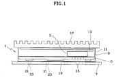
- a cooling object electronic element is a PAM 3 of CDMA modem 1.
- the CDMA modem 1 is largely comprised of an inner circuit substrate 5 and an external circuit substrate 7.
- the present invention can be applied to a case of a single circuit substrate.
- the inner circuit substrate can be a single circuit substrate.
- the structure according to the embodiment of the present invention comprises: an inner bafflement 9 and a baffle case 11 for baffling an inner circuit substrate 5, the inner bafflement 9 formed with an extended portion 13 for contacting an upper surface of a PAM 3 which is a cooling object electronic element mounted at the inner circuit substrate 5; a plurality of through holes 15 at the inner circuit substrate 5 underneath the PAM 3; a radiating plate 17 mounted on the baffle case 11 encompassing an external side of the inner bafflement 9 and the inner circuit substrate 5; and a plurality of baffle case holes 21 mounted underneath the baffle case 11.
- the bottom surface of the baffle case 11 contacts the upper surface of the external circuit substrate 7, where the upper surface of the external circuit substrate 7 contacting the bottom surface of the baffle case 11 is equipped with a metal cooling surface 19 as depicted in Fig. 4, and the external circuit substrate 7 is formed with a plurality of external circuit substrate holes 23 to correspondingly communicate with the baffle case holes 21 of the baffle case 11.
- the metal cooling surface 19 is a flat surface made of lead formed on the external circuit substrate 7 by a Solder Masking Open process so as to be automatically formed by soldering the circuit substrate.
- the extension of the inner bafflement 9 directly contacting the upper surface of the PAM 3 serves to swiftly discharge the heat generated from the PAM 3 by way of conduction.
- the plural holes 15 made of metal cylinders for communicating the upper and lower sides of the inner circuit substrate 5 are used for electrically connecting the upper and lower sides of the inner circuit substrate 5 and concurrently act as media for transferring the heat generated from the electronic element thus explained.
- the heat passing through the extension of the inner bafflement 9 and the through holes 15 of the inner circuit substrate 5 is emitted outside via the baffle case 11, where the heat is swiftly exhausted outside by the radiating plate 17 mounted on the baffle case 11, the baffle case holes 21 equipped at the bottom surface of the baffle case 11 and the metal cooling surface 19.
- a swift heat exchange is carried out by the surrounding air by a broad cooling area formed by a plurality of fins at the radiating plate 17, and heated air formed inside the baffle case 11 is swiftly released outside via the baffle case holes 2 to thereby promote an effective cooling of the inner circuit substrate 5 and the PAM 3.
- baffle case 11 makes contact with the metal cooling surface 19 provided at the external circuit substrate 7, heat can be also discharged outside by conduction via the metal cooling surface 19, and air heated inside the baffle case 11 passes through the baffle case 11 and the external circuit substrate 7 all together to be emitted outside.
- Heat can be transferred via a conduction route which is formed by the PAM3-extended portion 13-inner bafflement 9-baffle case 11-radiating plate 17, and a route which is formed by the PAM 3-extended portion 13-inner bafflement 9-baffle case 11-metal cooling surface 19 of the external circuit substrate 7, while the heat can be transferred via a convection route which is formed by the PAM 3-through holes 15-baffle case holes 21-external circuit substrate holes 23.
Landscapes
- Physics & Mathematics (AREA)
- Thermal Sciences (AREA)
- Engineering & Computer Science (AREA)
- Microelectronics & Electronic Packaging (AREA)
- Cooling Or The Like Of Electrical Apparatus (AREA)
- Shielding Devices Or Components To Electric Or Magnetic Fields (AREA)
- Cooling Or The Like Of Semiconductors Or Solid State Devices (AREA)
Applications Claiming Priority (2)
| Application Number | Priority Date | Filing Date | Title |
|---|---|---|---|
| KR10-2003-0063971A KR100534968B1 (ko) | 2003-09-16 | 2003-09-16 | 전자소자의 냉각구조 |
| KR2003063971 | 2003-09-16 |
Publications (3)
| Publication Number | Publication Date |
|---|---|
| EP1517602A2 true EP1517602A2 (de) | 2005-03-23 |
| EP1517602A3 EP1517602A3 (de) | 2008-03-05 |
| EP1517602B1 EP1517602B1 (de) | 2011-10-19 |
Family
ID=34192226
Family Applications (1)
| Application Number | Title | Priority Date | Filing Date |
|---|---|---|---|
| EP03028706A Expired - Lifetime EP1517602B1 (de) | 2003-09-16 | 2003-12-12 | Struktur zur Kühlung eines elektonischen Elementes |
Country Status (5)
| Country | Link |
|---|---|
| US (1) | US20050057903A1 (de) |
| EP (1) | EP1517602B1 (de) |
| JP (1) | JP2005093973A (de) |
| KR (1) | KR100534968B1 (de) |
| CN (1) | CN100361294C (de) |
Families Citing this family (29)
| Publication number | Priority date | Publication date | Assignee | Title |
|---|---|---|---|---|
| JP2006214861A (ja) * | 2005-02-03 | 2006-08-17 | Shimadzu Corp | 二次元画像検出器 |
| CN100524708C (zh) * | 2005-12-30 | 2009-08-05 | 财团法人工业技术研究院 | 直下式面光源模块用的基板及具有该基板的散热装置 |
| SE533704C2 (sv) | 2008-12-05 | 2010-12-07 | Flatfrog Lab Ab | Pekkänslig apparat och förfarande för drivning av densamma |
| EP2466428A3 (de) * | 2010-12-16 | 2015-07-29 | FlatFrog Laboratories AB | Berührungsvorrichtung mit getrennten Einsätzen |
| EP2466429A1 (de) | 2010-12-16 | 2012-06-20 | FlatFrog Laboratories AB | FTIR-Scansysteme zur Berührungserkennung |
| US10168835B2 (en) | 2012-05-23 | 2019-01-01 | Flatfrog Laboratories Ab | Spatial resolution in touch displays |
| US10019113B2 (en) | 2013-04-11 | 2018-07-10 | Flatfrog Laboratories Ab | Tomographic processing for touch detection |
| US9874978B2 (en) | 2013-07-12 | 2018-01-23 | Flatfrog Laboratories Ab | Partial detect mode |
| US10126882B2 (en) | 2014-01-16 | 2018-11-13 | Flatfrog Laboratories Ab | TIR-based optical touch systems of projection-type |
| WO2015108479A1 (en) | 2014-01-16 | 2015-07-23 | Flatfrog Laboratories Ab | Light coupling in tir-based optical touch systems |
| US10161886B2 (en) | 2014-06-27 | 2018-12-25 | Flatfrog Laboratories Ab | Detection of surface contamination |
| CN107209608A (zh) | 2015-01-28 | 2017-09-26 | 平蛙实验室股份公司 | 动态触摸隔离帧 |
| US10318074B2 (en) | 2015-01-30 | 2019-06-11 | Flatfrog Laboratories Ab | Touch-sensing OLED display with tilted emitters |
| EP3256936A4 (de) | 2015-02-09 | 2018-10-17 | FlatFrog Laboratories AB | Optisches berührungssystem mit mitteln zur projektion und detektion von lichtstrahlen über und in einer durchlässigen platte |
| WO2016140612A1 (en) | 2015-03-02 | 2016-09-09 | Flatfrog Laboratories Ab | Optical component for light coupling |
| US10775937B2 (en) | 2015-12-09 | 2020-09-15 | Flatfrog Laboratories Ab | Stylus identification |
| CN110100226A (zh) | 2016-11-24 | 2019-08-06 | 平蛙实验室股份公司 | 触摸信号的自动优化 |
| EP3667475B1 (de) | 2016-12-07 | 2022-09-07 | FlatFrog Laboratories AB | Krumme berührungsvorrichtung |
| CN116679845A (zh) | 2017-02-06 | 2023-09-01 | 平蛙实验室股份公司 | 触摸感测装置 |
| WO2018174786A1 (en) | 2017-03-22 | 2018-09-27 | Flatfrog Laboratories | Pen differentiation for touch displays |
| WO2018182476A1 (en) | 2017-03-28 | 2018-10-04 | Flatfrog Laboratories Ab | Touch sensing apparatus and method for assembly |
| EP3676694A4 (de) | 2017-09-01 | 2021-06-09 | FlatFrog Laboratories AB | Verbesserte optische komponente |
| US11567610B2 (en) | 2018-03-05 | 2023-01-31 | Flatfrog Laboratories Ab | Detection line broadening |
| WO2020080992A1 (en) | 2018-10-20 | 2020-04-23 | Flatfrog Laboratories Ab | Frame for a touch-sensitive device and tool therefor |
| WO2020153890A1 (en) | 2019-01-25 | 2020-07-30 | Flatfrog Laboratories Ab | A videoconferencing terminal and method of operating the same |
| US12056316B2 (en) | 2019-11-25 | 2024-08-06 | Flatfrog Laboratories Ab | Touch-sensing apparatus |
| EP4100822A4 (de) | 2020-02-08 | 2024-02-28 | FlatFrog Laboratories AB | Berührungsgerät mit interaktionen mit niedriger latenzzeit |
| CN121614054A (zh) | 2020-02-10 | 2026-03-06 | 平蛙实验室股份公司 | 触摸感测设备和制造触摸感测设备的框架元件的方法 |
| CN113795097A (zh) * | 2021-07-20 | 2021-12-14 | 山东环维通讯科技有限公司 | 一种基于通用流程的控制方法及具有该方法的控制设备 |
Family Cites Families (16)
| Publication number | Priority date | Publication date | Assignee | Title |
|---|---|---|---|---|
| JPS5931046A (ja) * | 1982-08-13 | 1984-02-18 | Mitsubishi Electric Corp | 半導体装置 |
| US4839774A (en) * | 1988-01-25 | 1989-06-13 | Digital Equipment Corporation | Apparatus and method for cooling electronic component packages using an array of directed nozzles fabricated in the circuit board |
| US5213868A (en) * | 1991-08-13 | 1993-05-25 | Chomerics, Inc. | Thermally conductive interface materials and methods of using the same |
| US6031723A (en) * | 1994-08-18 | 2000-02-29 | Allen-Bradley Company, Llc | Insulated surface mount circuit board construction |
| US5585671A (en) * | 1994-10-07 | 1996-12-17 | Nagesh; Voddarahalli K. | Reliable low thermal resistance package for high power flip clip ICs |
| JP2914342B2 (ja) * | 1997-03-28 | 1999-06-28 | 日本電気株式会社 | 集積回路装置の冷却構造 |
| JPH11204970A (ja) * | 1998-01-12 | 1999-07-30 | Alps Electric Co Ltd | 電子機器 |
| US6043983A (en) * | 1998-06-17 | 2000-03-28 | Intel Corporation | EMI containment for microprocessor core mounted on a card using surface mounted clips |
| US6058013A (en) * | 1998-07-02 | 2000-05-02 | Motorola Inc. | Molded housing with integral heatsink |
| US6086788A (en) * | 1999-03-15 | 2000-07-11 | Alliedsignal Inc. | Hydrofluorocarbon blown foam and method for preparation thereof |
| US6297441B1 (en) * | 2000-03-24 | 2001-10-02 | Chris Macris | Thermoelectric device and method of manufacture |
| EP1178594B1 (de) * | 2000-08-01 | 2009-08-12 | Mitsubishi Denki Kabushiki Kaisha | Elektronisches Gerät mit einem Substrat für die Schaltung |
| US6630743B2 (en) * | 2001-02-27 | 2003-10-07 | International Business Machines Corporation | Copper plated PTH barrels and methods for fabricating |
| JP3960115B2 (ja) * | 2001-05-24 | 2007-08-15 | 松下電器産業株式会社 | 携帯用電力増幅器 |
| DE10141697A1 (de) * | 2001-08-25 | 2003-03-06 | Bosch Gmbh Robert | Schalt- oder Steuergerät |
| US6727193B2 (en) * | 2002-03-08 | 2004-04-27 | Sun Microsystems, Inc. | Apparatus and methods for enhancing thermal performance of integrated circuit packages |
-
2003
- 2003-09-16 KR KR10-2003-0063971A patent/KR100534968B1/ko not_active Expired - Lifetime
- 2003-12-09 JP JP2003410919A patent/JP2005093973A/ja active Pending
- 2003-12-12 EP EP03028706A patent/EP1517602B1/de not_active Expired - Lifetime
- 2003-12-30 US US10/749,206 patent/US20050057903A1/en not_active Abandoned
- 2003-12-30 CN CNB2003101238127A patent/CN100361294C/zh not_active Expired - Fee Related
Also Published As
| Publication number | Publication date |
|---|---|
| EP1517602B1 (de) | 2011-10-19 |
| JP2005093973A (ja) | 2005-04-07 |
| KR100534968B1 (ko) | 2005-12-08 |
| EP1517602A3 (de) | 2008-03-05 |
| CN100361294C (zh) | 2008-01-09 |
| KR20050027633A (ko) | 2005-03-21 |
| US20050057903A1 (en) | 2005-03-17 |
| CN1610104A (zh) | 2005-04-27 |
Similar Documents
| Publication | Publication Date | Title |
|---|---|---|
| EP1517602B1 (de) | Struktur zur Kühlung eines elektonischen Elementes | |
| KR100299002B1 (ko) | 적층 반도체 장치 | |
| US8283773B2 (en) | Semiconductor device having anti-warping sheet | |
| US20100307730A1 (en) | Liquid-cooled heat dissipating device and method of making the same | |
| US20090059524A1 (en) | Heat dissipation device | |
| US20070090737A1 (en) | Light-emitting diode assembly and method of fabrication | |
| US11817372B2 (en) | Heat sink device | |
| CA2440522A1 (en) | Electronic module including a cooling substrate and related methods | |
| JP2002544469A (ja) | 貫通取付け穴を具えた集積回路のヒートパイプ用熱拡散装置 | |
| KR20030091275A (ko) | 리드 방열 세라믹 패키지 | |
| US20070133175A1 (en) | Heat dissipation device | |
| JP3126337U (ja) | 大型ledランプ | |
| WO2008029858A1 (fr) | Boîtier de semiconducteur et assemblage de boîtier de semiconducteur | |
| JP2001244391A (ja) | マルチチップモジュールの冷却構造 | |
| US6930883B2 (en) | Heat-dispersing module of electronic device | |
| KR100818745B1 (ko) | 냉각장치를 가진 발광다이오드 모듈 | |
| US7047757B2 (en) | Vacuum laser constant temperature device | |
| WO1999053256A1 (fr) | Tuyau de chauffage de type a plaques et structure d'installation correspondante | |
| JP2005005483A (ja) | 高輝度発光素子 | |
| CN224098150U (zh) | 一种高散热性的集成电路封装结构 | |
| TWI708545B (zh) | 可撓的散熱器、電子裝置、以及散熱方法 | |
| JP4404861B2 (ja) | 熱発生構成要素を冷却する装置、及び熱発生構成要素を冷却する装置を製造する方法 | |
| CN224098031U (zh) | 一种散热组件以及换热器 | |
| JP4496491B2 (ja) | 電子機器 | |
| JPH08125364A (ja) | 半導体部品の放熱構造 |
Legal Events
| Date | Code | Title | Description |
|---|---|---|---|
| PUAI | Public reference made under article 153(3) epc to a published international application that has entered the european phase |
Free format text: ORIGINAL CODE: 0009012 |
|
| AK | Designated contracting states |
Kind code of ref document: A2 Designated state(s): AT BE BG CH CY CZ DE DK EE ES FI FR GB GR HU IE IT LI LU MC NL PT RO SE SI SK TR |
|
| AX | Request for extension of the european patent |
Extension state: AL LT LV MK |
|
| PUAL | Search report despatched |
Free format text: ORIGINAL CODE: 0009013 |
|
| AK | Designated contracting states |
Kind code of ref document: A3 Designated state(s): AT BE BG CH CY CZ DE DK EE ES FI FR GB GR HU IE IT LI LU MC NL PT RO SE SI SK TR |
|
| AX | Request for extension of the european patent |
Extension state: AL LT LV MK |
|
| 17P | Request for examination filed |
Effective date: 20080424 |
|
| AKX | Designation fees paid |
Designated state(s): DE FR GB |
|
| 17Q | First examination report despatched |
Effective date: 20100831 |
|
| GRAP | Despatch of communication of intention to grant a patent |
Free format text: ORIGINAL CODE: EPIDOSNIGR1 |
|
| GRAS | Grant fee paid |
Free format text: ORIGINAL CODE: EPIDOSNIGR3 |
|
| GRAA | (expected) grant |
Free format text: ORIGINAL CODE: 0009210 |
|
| AK | Designated contracting states |
Kind code of ref document: B1 Designated state(s): DE FR GB |
|
| REG | Reference to a national code |
Ref country code: GB Ref legal event code: FG4D |
|
| REG | Reference to a national code |
Ref country code: DE Ref legal event code: R096 Ref document number: 60338798 Country of ref document: DE Effective date: 20111222 |
|
| PLBE | No opposition filed within time limit |
Free format text: ORIGINAL CODE: 0009261 |
|
| STAA | Information on the status of an ep patent application or granted ep patent |
Free format text: STATUS: NO OPPOSITION FILED WITHIN TIME LIMIT |
|
| 26N | No opposition filed |
Effective date: 20120720 |
|
| REG | Reference to a national code |
Ref country code: DE Ref legal event code: R097 Ref document number: 60338798 Country of ref document: DE Effective date: 20120720 |
|
| REG | Reference to a national code |
Ref country code: FR Ref legal event code: PLFP Year of fee payment: 13 |
|
| REG | Reference to a national code |
Ref country code: FR Ref legal event code: PLFP Year of fee payment: 14 |
|
| REG | Reference to a national code |
Ref country code: FR Ref legal event code: PLFP Year of fee payment: 15 |
|
| PGFP | Annual fee paid to national office [announced via postgrant information from national office to epo] |
Ref country code: FR Payment date: 20211125 Year of fee payment: 19 Ref country code: GB Payment date: 20211122 Year of fee payment: 19 |
|
| PGFP | Annual fee paid to national office [announced via postgrant information from national office to epo] |
Ref country code: DE Payment date: 20220621 Year of fee payment: 20 |
|
| P01 | Opt-out of the competence of the unified patent court (upc) registered |
Effective date: 20230512 |
|
| GBPC | Gb: european patent ceased through non-payment of renewal fee |
Effective date: 20221212 |
|
| PG25 | Lapsed in a contracting state [announced via postgrant information from national office to epo] |
Ref country code: GB Free format text: LAPSE BECAUSE OF NON-PAYMENT OF DUE FEES Effective date: 20221212 |
|
| PG25 | Lapsed in a contracting state [announced via postgrant information from national office to epo] |
Ref country code: FR Free format text: LAPSE BECAUSE OF NON-PAYMENT OF DUE FEES Effective date: 20221231 |
|
| REG | Reference to a national code |
Ref country code: DE Ref legal event code: R071 Ref document number: 60338798 Country of ref document: DE |