EP1516208B1 - Planar optical waveguide assembly and method of preparing same - Google Patents
Planar optical waveguide assembly and method of preparing same Download PDFInfo
- Publication number
- EP1516208B1 EP1516208B1 EP03719514.6A EP03719514A EP1516208B1 EP 1516208 B1 EP1516208 B1 EP 1516208B1 EP 03719514 A EP03719514 A EP 03719514A EP 1516208 B1 EP1516208 B1 EP 1516208B1
- Authority
- EP
- European Patent Office
- Prior art keywords
- silicone
- film
- units
- clad layer
- sio
- Prior art date
- Legal status (The legal status is an assumption and is not a legal conclusion. Google has not performed a legal analysis and makes no representation as to the accuracy of the status listed.)
- Expired - Lifetime
Links
- 238000000034 method Methods 0.000 title claims description 77
- 230000003287 optical effect Effects 0.000 title claims description 33
- 229920001296 polysiloxane Polymers 0.000 claims description 134
- 239000000203 mixture Substances 0.000 claims description 129
- 239000002904 solvent Substances 0.000 claims description 41
- 229920000642 polymer Polymers 0.000 claims description 37
- 239000003054 catalyst Substances 0.000 claims description 33
- 229920006254 polymer film Polymers 0.000 claims description 25
- 229920006268 silicone film Polymers 0.000 claims description 25
- 239000000758 substrate Substances 0.000 claims description 25
- 125000003342 alkenyl group Chemical group 0.000 claims description 23
- 239000011347 resin Substances 0.000 claims description 22
- 229920005989 resin Polymers 0.000 claims description 22
- 125000004435 hydrogen atom Chemical group [H]* 0.000 claims description 21
- 238000006459 hydrosilylation reaction Methods 0.000 claims description 20
- 125000001183 hydrocarbyl group Chemical group 0.000 claims description 19
- 229910020388 SiO1/2 Inorganic materials 0.000 claims description 17
- 230000005855 radiation Effects 0.000 claims description 16
- 150000003961 organosilicon compounds Chemical class 0.000 claims description 14
- 229910020487 SiO3/2 Inorganic materials 0.000 claims description 13
- 238000010438 heat treatment Methods 0.000 claims description 10
- HRGDZIGMBDGFTC-UHFFFAOYSA-N platinum(2+) Chemical group [Pt+2] HRGDZIGMBDGFTC-UHFFFAOYSA-N 0.000 claims description 10
- 125000001931 aliphatic group Chemical group 0.000 claims description 6
- 230000003197 catalytic effect Effects 0.000 claims description 6
- 239000010408 film Substances 0.000 description 52
- 239000010410 layer Substances 0.000 description 45
- -1 polyethylene Polymers 0.000 description 35
- BASFCYQUMIYNBI-UHFFFAOYSA-N platinum Chemical compound [Pt] BASFCYQUMIYNBI-UHFFFAOYSA-N 0.000 description 30
- 235000012431 wafers Nutrition 0.000 description 29
- 229910052751 metal Inorganic materials 0.000 description 11
- 239000002184 metal Substances 0.000 description 11
- 230000014759 maintenance of location Effects 0.000 description 10
- YXFVVABEGXRONW-UHFFFAOYSA-N Toluene Chemical compound CC1=CC=CC=C1 YXFVVABEGXRONW-UHFFFAOYSA-N 0.000 description 9
- 239000003112 inhibitor Substances 0.000 description 9
- AUHZEENZYGFFBQ-UHFFFAOYSA-N mesitylene Substances CC1=CC(C)=CC(C)=C1 AUHZEENZYGFFBQ-UHFFFAOYSA-N 0.000 description 9
- 125000001827 mesitylenyl group Chemical group [H]C1=C(C(*)=C(C([H])=C1C([H])([H])[H])C([H])([H])[H])C([H])([H])[H] 0.000 description 9
- 229910020485 SiO4/2 Inorganic materials 0.000 description 8
- 229910052697 platinum Inorganic materials 0.000 description 8
- 125000004432 carbon atom Chemical group C* 0.000 description 7
- 230000005494 condensation Effects 0.000 description 7
- 125000002496 methyl group Chemical group [H]C([H])([H])* 0.000 description 7
- 229920001843 polymethylhydrosiloxane Polymers 0.000 description 7
- VEJOYRPGKZZTJW-FDGPNNRMSA-N (z)-4-hydroxypent-3-en-2-one;platinum Chemical compound [Pt].C\C(O)=C\C(C)=O.C\C(O)=C\C(C)=O VEJOYRPGKZZTJW-FDGPNNRMSA-N 0.000 description 6
- 229910020447 SiO2/2 Inorganic materials 0.000 description 6
- VYPSYNLAJGMNEJ-UHFFFAOYSA-N Silicium dioxide Chemical compound O=[Si]=O VYPSYNLAJGMNEJ-UHFFFAOYSA-N 0.000 description 6
- XUIMIQQOPSSXEZ-UHFFFAOYSA-N Silicon Chemical compound [Si] XUIMIQQOPSSXEZ-UHFFFAOYSA-N 0.000 description 6
- 238000009833 condensation Methods 0.000 description 6
- 238000004519 manufacturing process Methods 0.000 description 6
- 229910052710 silicon Inorganic materials 0.000 description 6
- 239000010703 silicon Substances 0.000 description 6
- 238000004528 spin coating Methods 0.000 description 6
- 239000004698 Polyethylene Substances 0.000 description 5
- 150000001875 compounds Chemical class 0.000 description 5
- 239000000463 material Substances 0.000 description 5
- 229920000573 polyethylene Polymers 0.000 description 5
- DURPTKYDGMDSBL-UHFFFAOYSA-N 1-butoxybutane Chemical compound CCCCOCCCC DURPTKYDGMDSBL-UHFFFAOYSA-N 0.000 description 4
- 239000009261 D 400 Substances 0.000 description 4
- 238000007796 conventional method Methods 0.000 description 4
- KPUWHANPEXNPJT-UHFFFAOYSA-N disiloxane Chemical class [SiH3]O[SiH3] KPUWHANPEXNPJT-UHFFFAOYSA-N 0.000 description 4
- 239000004615 ingredient Substances 0.000 description 4
- 238000005259 measurement Methods 0.000 description 4
- BKIMMITUMNQMOS-UHFFFAOYSA-N nonane Chemical compound CCCCCCCCC BKIMMITUMNQMOS-UHFFFAOYSA-N 0.000 description 4
- 239000003960 organic solvent Substances 0.000 description 4
- 238000005507 spraying Methods 0.000 description 4
- 239000000126 substance Substances 0.000 description 4
- SNRUBQQJIBEYMU-UHFFFAOYSA-N Dodecane Natural products CCCCCCCCCCCC SNRUBQQJIBEYMU-UHFFFAOYSA-N 0.000 description 3
- XEKOWRVHYACXOJ-UHFFFAOYSA-N Ethyl acetate Chemical compound CCOC(C)=O XEKOWRVHYACXOJ-UHFFFAOYSA-N 0.000 description 3
- KDLHZDBZIXYQEI-UHFFFAOYSA-N Palladium Chemical compound [Pd] KDLHZDBZIXYQEI-UHFFFAOYSA-N 0.000 description 3
- BLRPTPMANUNPDV-UHFFFAOYSA-N Silane Chemical compound [SiH4] BLRPTPMANUNPDV-UHFFFAOYSA-N 0.000 description 3
- 229910052782 aluminium Inorganic materials 0.000 description 3
- XAGFODPZIPBFFR-UHFFFAOYSA-N aluminium Chemical compound [Al] XAGFODPZIPBFFR-UHFFFAOYSA-N 0.000 description 3
- 230000001680 brushing effect Effects 0.000 description 3
- 239000003060 catalysis inhibitor Substances 0.000 description 3
- 238000006243 chemical reaction Methods 0.000 description 3
- 125000004122 cyclic group Chemical group 0.000 description 3
- 238000007598 dipping method Methods 0.000 description 3
- 230000007613 environmental effect Effects 0.000 description 3
- 239000000706 filtrate Substances 0.000 description 3
- 239000011888 foil Substances 0.000 description 3
- 229920006136 organohydrogenpolysiloxane Polymers 0.000 description 3
- 150000001282 organosilanes Chemical class 0.000 description 3
- 125000001997 phenyl group Chemical group [H]C1=C([H])C([H])=C(*)C([H])=C1[H] 0.000 description 3
- 238000007650 screen-printing Methods 0.000 description 3
- 150000004756 silanes Chemical class 0.000 description 3
- 239000010409 thin film Substances 0.000 description 3
- VYXHVRARDIDEHS-UHFFFAOYSA-N 1,5-cyclooctadiene Chemical compound C1CC=CCCC=C1 VYXHVRARDIDEHS-UHFFFAOYSA-N 0.000 description 2
- 239000004912 1,5-cyclooctadiene Substances 0.000 description 2
- YEJRWHAVMIAJKC-UHFFFAOYSA-N 4-Butyrolactone Chemical compound O=C1CCCO1 YEJRWHAVMIAJKC-UHFFFAOYSA-N 0.000 description 2
- IJGRMHOSHXDMSA-UHFFFAOYSA-N Atomic nitrogen Chemical compound N#N IJGRMHOSHXDMSA-UHFFFAOYSA-N 0.000 description 2
- 239000005046 Chlorosilane Substances 0.000 description 2
- RTZKZFJDLAIYFH-UHFFFAOYSA-N Diethyl ether Chemical compound CCOCC RTZKZFJDLAIYFH-UHFFFAOYSA-N 0.000 description 2
- 206010073306 Exposure to radiation Diseases 0.000 description 2
- VEXZGXHMUGYJMC-UHFFFAOYSA-N Hydrochloric acid Chemical compound Cl VEXZGXHMUGYJMC-UHFFFAOYSA-N 0.000 description 2
- 239000004677 Nylon Substances 0.000 description 2
- 239000004952 Polyamide Substances 0.000 description 2
- 239000004642 Polyimide Substances 0.000 description 2
- 239000004743 Polypropylene Substances 0.000 description 2
- 229910003910 SiCl4 Inorganic materials 0.000 description 2
- 238000007259 addition reaction Methods 0.000 description 2
- 150000001298 alcohols Chemical class 0.000 description 2
- 150000004945 aromatic hydrocarbons Chemical class 0.000 description 2
- 230000005540 biological transmission Effects 0.000 description 2
- 239000011203 carbon fibre reinforced carbon Substances 0.000 description 2
- 239000003153 chemical reaction reagent Substances 0.000 description 2
- KOPOQZFJUQMUML-UHFFFAOYSA-N chlorosilane Chemical compound Cl[SiH3] KOPOQZFJUQMUML-UHFFFAOYSA-N 0.000 description 2
- 239000011248 coating agent Substances 0.000 description 2
- 238000000576 coating method Methods 0.000 description 2
- 229920001577 copolymer Polymers 0.000 description 2
- NNBZCPXTIHJBJL-UHFFFAOYSA-N decalin Chemical compound C1CCCC2CCCCC21 NNBZCPXTIHJBJL-UHFFFAOYSA-N 0.000 description 2
- 235000013870 dimethyl polysiloxane Nutrition 0.000 description 2
- 238000004090 dissolution Methods 0.000 description 2
- 230000000694 effects Effects 0.000 description 2
- 239000003822 epoxy resin Substances 0.000 description 2
- 150000002148 esters Chemical class 0.000 description 2
- 238000005530 etching Methods 0.000 description 2
- CATSNJVOTSVZJV-UHFFFAOYSA-N heptan-2-one Chemical compound CCCCCC(C)=O CATSNJVOTSVZJV-UHFFFAOYSA-N 0.000 description 2
- 230000007062 hydrolysis Effects 0.000 description 2
- 238000006460 hydrolysis reaction Methods 0.000 description 2
- 150000002576 ketones Chemical class 0.000 description 2
- 150000002688 maleic acid derivatives Chemical class 0.000 description 2
- 229920001778 nylon Polymers 0.000 description 2
- 125000000962 organic group Chemical group 0.000 description 2
- 229920002120 photoresistant polymer Polymers 0.000 description 2
- 229920000435 poly(dimethylsiloxane) Polymers 0.000 description 2
- 229920000548 poly(silane) polymer Polymers 0.000 description 2
- 229920002647 polyamide Polymers 0.000 description 2
- 229920000647 polyepoxide Polymers 0.000 description 2
- 229920000728 polyester Polymers 0.000 description 2
- 229920001721 polyimide Polymers 0.000 description 2
- 229920000098 polyolefin Polymers 0.000 description 2
- 229920001155 polypropylene Polymers 0.000 description 2
- 238000013404 process transfer Methods 0.000 description 2
- 239000010948 rhodium Substances 0.000 description 2
- 239000000377 silicon dioxide Substances 0.000 description 2
- 235000012239 silicon dioxide Nutrition 0.000 description 2
- FDNAPBUWERUEDA-UHFFFAOYSA-N silicon tetrachloride Chemical compound Cl[Si](Cl)(Cl)Cl FDNAPBUWERUEDA-UHFFFAOYSA-N 0.000 description 2
- 239000000243 solution Substances 0.000 description 2
- 229910052723 transition metal Inorganic materials 0.000 description 2
- AYNNSCRYTDRFCP-UHFFFAOYSA-N triazene Chemical compound NN=N AYNNSCRYTDRFCP-UHFFFAOYSA-N 0.000 description 2
- 125000000391 vinyl group Chemical group [H]C([*])=C([H])[H] 0.000 description 2
- 229920002554 vinyl polymer Polymers 0.000 description 2
- 239000008096 xylene Substances 0.000 description 2
- UHXCHUWSQRLZJS-UHFFFAOYSA-N (4-dimethylsilylidenecyclohexa-2,5-dien-1-ylidene)-dimethylsilane Chemical compound C[Si](C)C1=CC=C([Si](C)C)C=C1 UHXCHUWSQRLZJS-UHFFFAOYSA-N 0.000 description 1
- KWEKXPWNFQBJAY-UHFFFAOYSA-N (dimethyl-$l^{3}-silanyl)oxy-dimethylsilicon Chemical compound C[Si](C)O[Si](C)C KWEKXPWNFQBJAY-UHFFFAOYSA-N 0.000 description 1
- HMVBQEAJQVQOTI-SOFGYWHQSA-N (e)-3,5-dimethylhex-3-en-1-yne Chemical compound CC(C)\C=C(/C)C#C HMVBQEAJQVQOTI-SOFGYWHQSA-N 0.000 description 1
- GRGVQLWQXHFRHO-AATRIKPKSA-N (e)-3-methylpent-3-en-1-yne Chemical compound C\C=C(/C)C#C GRGVQLWQXHFRHO-AATRIKPKSA-N 0.000 description 1
- QYLFHLNFIHBCPR-UHFFFAOYSA-N 1-ethynylcyclohexan-1-ol Chemical compound C#CC1(O)CCCCC1 QYLFHLNFIHBCPR-UHFFFAOYSA-N 0.000 description 1
- VLQZJOLYNOGECD-UHFFFAOYSA-N 2,4,6-trimethyl-1,3,5,2,4,6-trioxatrisilinane Chemical compound C[SiH]1O[SiH](C)O[SiH](C)O1 VLQZJOLYNOGECD-UHFFFAOYSA-N 0.000 description 1
- XNWFRZJHXBZDAG-UHFFFAOYSA-N 2-METHOXYETHANOL Chemical compound COCCO XNWFRZJHXBZDAG-UHFFFAOYSA-N 0.000 description 1
- MAYUMUDTQDNZBD-UHFFFAOYSA-N 2-chloroethylsilane Chemical compound [SiH3]CCCl MAYUMUDTQDNZBD-UHFFFAOYSA-N 0.000 description 1
- 125000004493 2-methylbut-1-yl group Chemical group CC(C*)CC 0.000 description 1
- KSLSOBUAIFEGLT-UHFFFAOYSA-N 2-phenylbut-3-yn-2-ol Chemical compound C#CC(O)(C)C1=CC=CC=C1 KSLSOBUAIFEGLT-UHFFFAOYSA-N 0.000 description 1
- 125000000094 2-phenylethyl group Chemical group [H]C1=C([H])C([H])=C(C([H])=C1[H])C([H])([H])C([H])([H])* 0.000 description 1
- 125000003903 2-propenyl group Chemical group [H]C([*])([H])C([H])=C([H])[H] 0.000 description 1
- NECRQCBKTGZNMH-UHFFFAOYSA-N 3,5-dimethylhex-1-yn-3-ol Chemical compound CC(C)CC(C)(O)C#C NECRQCBKTGZNMH-UHFFFAOYSA-N 0.000 description 1
- 125000003542 3-methylbutan-2-yl group Chemical group [H]C([H])([H])C([H])(*)C([H])(C([H])([H])[H])C([H])([H])[H] 0.000 description 1
- 239000004925 Acrylic resin Substances 0.000 description 1
- 229920000178 Acrylic resin Polymers 0.000 description 1
- JBRZTFJDHDCESZ-UHFFFAOYSA-N AsGa Chemical compound [As]#[Ga] JBRZTFJDHDCESZ-UHFFFAOYSA-N 0.000 description 1
- LHRBHFVFUACXIJ-UHFFFAOYSA-N C[SiH](C)C1=CC([SiH](C)C)=CC([SiH](C)C)=C1 Chemical compound C[SiH](C)C1=CC([SiH](C)C)=CC([SiH](C)C)=C1 LHRBHFVFUACXIJ-UHFFFAOYSA-N 0.000 description 1
- 239000004215 Carbon black (E152) Substances 0.000 description 1
- 239000004971 Cross linker Substances 0.000 description 1
- 229910001218 Gallium arsenide Inorganic materials 0.000 description 1
- UFHFLCQGNIYNRP-UHFFFAOYSA-N Hydrogen Chemical compound [H][H] UFHFLCQGNIYNRP-UHFFFAOYSA-N 0.000 description 1
- DGAQECJNVWCQMB-PUAWFVPOSA-M Ilexoside XXIX Chemical compound C[C@@H]1CC[C@@]2(CC[C@@]3(C(=CC[C@H]4[C@]3(CC[C@@H]5[C@@]4(CC[C@@H](C5(C)C)OS(=O)(=O)[O-])C)C)[C@@H]2[C@]1(C)O)C)C(=O)O[C@H]6[C@@H]([C@H]([C@@H]([C@H](O6)CO)O)O)O.[Na+] DGAQECJNVWCQMB-PUAWFVPOSA-M 0.000 description 1
- NTIZESTWPVYFNL-UHFFFAOYSA-N Methyl isobutyl ketone Chemical compound CC(C)CC(C)=O NTIZESTWPVYFNL-UHFFFAOYSA-N 0.000 description 1
- UIHCLUNTQKBZGK-UHFFFAOYSA-N Methyl isobutyl ketone Natural products CCC(C)C(C)=O UIHCLUNTQKBZGK-UHFFFAOYSA-N 0.000 description 1
- CTQNGGLPUBDAKN-UHFFFAOYSA-N O-Xylene Chemical compound CC1=CC=CC=C1C CTQNGGLPUBDAKN-UHFFFAOYSA-N 0.000 description 1
- 239000002202 Polyethylene glycol Substances 0.000 description 1
- 239000004793 Polystyrene Substances 0.000 description 1
- KJTLSVCANCCWHF-UHFFFAOYSA-N Ruthenium Chemical compound [Ru] KJTLSVCANCCWHF-UHFFFAOYSA-N 0.000 description 1
- BQCADISMDOOEFD-UHFFFAOYSA-N Silver Chemical compound [Ag] BQCADISMDOOEFD-UHFFFAOYSA-N 0.000 description 1
- 238000006621 Wurtz reaction Methods 0.000 description 1
- YKSADNUOSVJOAS-UHFFFAOYSA-N [bis[(dimethyl-$l^{3}-silanyl)oxy]-phenylsilyl]oxy-dimethylsilicon Chemical compound C[Si](C)O[Si](O[Si](C)C)(O[Si](C)C)C1=CC=CC=C1 YKSADNUOSVJOAS-UHFFFAOYSA-N 0.000 description 1
- ZFJFYUXFKXTXGT-UHFFFAOYSA-N [dimethyl(methylsilyloxy)silyl]oxy-[dimethyl(trimethylsilyloxy)silyl]oxy-dimethylsilane Chemical compound C[SiH2]O[Si](C)(C)O[Si](C)(C)O[Si](C)(C)O[Si](C)(C)C ZFJFYUXFKXTXGT-UHFFFAOYSA-N 0.000 description 1
- 239000002253 acid Substances 0.000 description 1
- 125000002015 acyclic group Chemical group 0.000 description 1
- 239000002318 adhesion promoter Substances 0.000 description 1
- 230000002411 adverse Effects 0.000 description 1
- 150000001338 aliphatic hydrocarbons Chemical class 0.000 description 1
- 150000004703 alkoxides Chemical class 0.000 description 1
- 125000002877 alkyl aryl group Chemical group 0.000 description 1
- 125000000217 alkyl group Chemical group 0.000 description 1
- 229920003180 amino resin Polymers 0.000 description 1
- 125000003710 aryl alkyl group Chemical group 0.000 description 1
- 125000003118 aryl group Chemical group 0.000 description 1
- 125000001797 benzyl group Chemical group [H]C1=C([H])C([H])=C(C([H])=C1[H])C([H])([H])* 0.000 description 1
- 238000009835 boiling Methods 0.000 description 1
- 125000004369 butenyl group Chemical group C(=CCC)* 0.000 description 1
- 125000000484 butyl group Chemical group [H]C([*])([H])C([H])([H])C([H])([H])C([H])([H])[H] 0.000 description 1
- 239000000919 ceramic Substances 0.000 description 1
- 125000001309 chloro group Chemical group Cl* 0.000 description 1
- 238000006482 condensation reaction Methods 0.000 description 1
- 238000004132 cross linking Methods 0.000 description 1
- 125000000753 cycloalkyl group Chemical group 0.000 description 1
- 125000000113 cyclohexyl group Chemical group [H]C1([H])C([H])([H])C([H])([H])C([H])(*)C([H])([H])C1([H])[H] 0.000 description 1
- 125000000058 cyclopentadienyl group Chemical group C1(=CC=CC1)* 0.000 description 1
- 125000001511 cyclopentyl group Chemical group [H]C1([H])C([H])([H])C([H])([H])C([H])(*)C1([H])[H] 0.000 description 1
- 238000000354 decomposition reaction Methods 0.000 description 1
- 125000002704 decyl group Chemical group [H]C([H])([H])C([H])([H])C([H])([H])C([H])([H])C([H])([H])C([H])([H])C([H])([H])C([H])([H])C([H])([H])C([H])([H])* 0.000 description 1
- 229910052805 deuterium Inorganic materials 0.000 description 1
- 125000004431 deuterium atom Chemical group 0.000 description 1
- 125000004188 dichlorophenyl group Chemical group 0.000 description 1
- 125000000118 dimethyl group Chemical group [H]C([H])([H])* 0.000 description 1
- 239000004205 dimethyl polysiloxane Substances 0.000 description 1
- VDCSGNNYCFPWFK-UHFFFAOYSA-N diphenylsilane Chemical compound C=1C=CC=CC=1[SiH2]C1=CC=CC=C1 VDCSGNNYCFPWFK-UHFFFAOYSA-N 0.000 description 1
- SCTQCPWFWDWNTC-UHFFFAOYSA-N diphenylsilyloxy(diphenyl)silane Chemical compound C=1C=CC=CC=1[SiH](C=1C=CC=CC=1)O[SiH](C=1C=CC=CC=1)C1=CC=CC=C1 SCTQCPWFWDWNTC-UHFFFAOYSA-N 0.000 description 1
- PZPGRFITIJYNEJ-UHFFFAOYSA-N disilane Chemical compound [SiH3][SiH3] PZPGRFITIJYNEJ-UHFFFAOYSA-N 0.000 description 1
- 125000003438 dodecyl group Chemical group [H]C([H])([H])C([H])([H])C([H])([H])C([H])([H])C([H])([H])C([H])([H])C([H])([H])C([H])([H])C([H])([H])C([H])([H])C([H])([H])C([H])([H])* 0.000 description 1
- 238000001035 drying Methods 0.000 description 1
- ZSWFCLXCOIISFI-UHFFFAOYSA-N endo-cyclopentadiene Natural products C1C=CC=C1 ZSWFCLXCOIISFI-UHFFFAOYSA-N 0.000 description 1
- 238000011067 equilibration Methods 0.000 description 1
- 150000002170 ethers Chemical class 0.000 description 1
- 125000001495 ethyl group Chemical group [H]C([H])([H])C([H])([H])* 0.000 description 1
- 239000012530 fluid Substances 0.000 description 1
- 229920002313 fluoropolymer Polymers 0.000 description 1
- VZCYOOQTPOCHFL-OWOJBTEDSA-L fumarate(2-) Chemical class [O-]C(=O)\C=C\C([O-])=O VZCYOOQTPOCHFL-OWOJBTEDSA-L 0.000 description 1
- 239000005350 fused silica glass Substances 0.000 description 1
- 239000011521 glass Substances 0.000 description 1
- 150000005826 halohydrocarbons Chemical class 0.000 description 1
- LNEPOXFFQSENCJ-UHFFFAOYSA-N haloperidol Chemical compound C1CC(O)(C=2C=CC(Cl)=CC=2)CCN1CCCC(=O)C1=CC=C(F)C=C1 LNEPOXFFQSENCJ-UHFFFAOYSA-N 0.000 description 1
- 125000003187 heptyl group Chemical group [H]C([*])([H])C([H])([H])C([H])([H])C([H])([H])C([H])([H])C([H])([H])C([H])([H])[H] 0.000 description 1
- 125000006038 hexenyl group Chemical group 0.000 description 1
- 125000004051 hexyl group Chemical group [H]C([H])([H])C([H])([H])C([H])([H])C([H])([H])C([H])([H])C([H])([H])* 0.000 description 1
- 229920001519 homopolymer Polymers 0.000 description 1
- 229930195733 hydrocarbon Natural products 0.000 description 1
- 150000002430 hydrocarbons Chemical class 0.000 description 1
- 229910052739 hydrogen Inorganic materials 0.000 description 1
- 239000001257 hydrogen Substances 0.000 description 1
- 125000002887 hydroxy group Chemical group [H]O* 0.000 description 1
- 238000007654 immersion Methods 0.000 description 1
- 239000011256 inorganic filler Substances 0.000 description 1
- 229910003475 inorganic filler Inorganic materials 0.000 description 1
- 229910052500 inorganic mineral Inorganic materials 0.000 description 1
- 229910052741 iridium Inorganic materials 0.000 description 1
- GKOZUEZYRPOHIO-UHFFFAOYSA-N iridium atom Chemical compound [Ir] GKOZUEZYRPOHIO-UHFFFAOYSA-N 0.000 description 1
- 125000000959 isobutyl group Chemical group [H]C([H])([H])C([H])(C([H])([H])[H])C([H])([H])* 0.000 description 1
- 125000001972 isopentyl group Chemical group [H]C([H])([H])C([H])(C([H])([H])[H])C([H])([H])C([H])([H])* 0.000 description 1
- 125000001449 isopropyl group Chemical group [H]C([H])([H])C([H])(*)C([H])([H])[H] 0.000 description 1
- 229910052744 lithium Inorganic materials 0.000 description 1
- 125000002960 margaryl group Chemical group [H]C([*])([H])C([H])([H])C([H])([H])C([H])([H])C([H])([H])C([H])([H])C([H])([H])C([H])([H])C([H])([H])C([H])([H])C([H])([H])C([H])([H])C([H])([H])C([H])([H])C([H])([H])C([H])([H])C([H])([H])[H] 0.000 description 1
- 239000012528 membrane Substances 0.000 description 1
- QSHDDOUJBYECFT-UHFFFAOYSA-N mercury Chemical compound [Hg] QSHDDOUJBYECFT-UHFFFAOYSA-N 0.000 description 1
- 229910052753 mercury Inorganic materials 0.000 description 1
- 125000000956 methoxy group Chemical group [H]C([H])([H])O* 0.000 description 1
- 125000002816 methylsulfanyl group Chemical group [H]C([H])([H])S[*] 0.000 description 1
- 239000011707 mineral Substances 0.000 description 1
- 125000001421 myristyl group Chemical group [H]C([*])([H])C([H])([H])C([H])([H])C([H])([H])C([H])([H])C([H])([H])C([H])([H])C([H])([H])C([H])([H])C([H])([H])C([H])([H])C([H])([H])C([H])([H])C([H])([H])[H] 0.000 description 1
- 125000001624 naphthyl group Chemical group 0.000 description 1
- 125000001971 neopentyl group Chemical group [H]C([*])([H])C(C([H])([H])[H])(C([H])([H])[H])C([H])([H])[H] 0.000 description 1
- 229910052757 nitrogen Inorganic materials 0.000 description 1
- 125000001400 nonyl group Chemical group [H]C([*])([H])C([H])([H])C([H])([H])C([H])([H])C([H])([H])C([H])([H])C([H])([H])C([H])([H])C([H])([H])[H] 0.000 description 1
- HMMGMWAXVFQUOA-UHFFFAOYSA-N octamethylcyclotetrasiloxane Chemical compound C[Si]1(C)O[Si](C)(C)O[Si](C)(C)O[Si](C)(C)O1 HMMGMWAXVFQUOA-UHFFFAOYSA-N 0.000 description 1
- 125000002347 octyl group Chemical group [H]C([*])([H])C([H])([H])C([H])([H])C([H])([H])C([H])([H])C([H])([H])C([H])([H])C([H])([H])[H] 0.000 description 1
- 229910052762 osmium Inorganic materials 0.000 description 1
- SYQBFIAQOQZEGI-UHFFFAOYSA-N osmium atom Chemical compound [Os] SYQBFIAQOQZEGI-UHFFFAOYSA-N 0.000 description 1
- 230000003647 oxidation Effects 0.000 description 1
- 238000007254 oxidation reaction Methods 0.000 description 1
- TWNQGVIAIRXVLR-UHFFFAOYSA-N oxo(oxoalumanyloxy)alumane Chemical compound O=[Al]O[Al]=O TWNQGVIAIRXVLR-UHFFFAOYSA-N 0.000 description 1
- 229910052763 palladium Inorganic materials 0.000 description 1
- 125000000913 palmityl group Chemical group [H]C([*])([H])C([H])([H])C([H])([H])C([H])([H])C([H])([H])C([H])([H])C([H])([H])C([H])([H])C([H])([H])C([H])([H])C([H])([H])C([H])([H])C([H])([H])C([H])([H])C([H])([H])C([H])([H])[H] 0.000 description 1
- 125000002958 pentadecyl group Chemical group [H]C([*])([H])C([H])([H])C([H])([H])C([H])([H])C([H])([H])C([H])([H])C([H])([H])C([H])([H])C([H])([H])C([H])([H])C([H])([H])C([H])([H])C([H])([H])C([H])([H])C([H])([H])[H] 0.000 description 1
- 125000003538 pentan-3-yl group Chemical group [H]C([H])([H])C([H])([H])C([H])(*)C([H])([H])C([H])([H])[H] 0.000 description 1
- 125000001147 pentyl group Chemical group C(CCCC)* 0.000 description 1
- 239000003504 photosensitizing agent Substances 0.000 description 1
- 229920003229 poly(methyl methacrylate) Polymers 0.000 description 1
- 229920003216 poly(methylphenylsiloxane) Polymers 0.000 description 1
- 229920002492 poly(sulfone) Polymers 0.000 description 1
- 229920000058 polyacrylate Polymers 0.000 description 1
- 239000004417 polycarbonate Substances 0.000 description 1
- 229920000515 polycarbonate Polymers 0.000 description 1
- 229920006393 polyether sulfone Polymers 0.000 description 1
- 229920001223 polyethylene glycol Polymers 0.000 description 1
- 230000000379 polymerizing effect Effects 0.000 description 1
- 239000004926 polymethyl methacrylate Substances 0.000 description 1
- 229920002223 polystyrene Polymers 0.000 description 1
- 229920001343 polytetrafluoroethylene Polymers 0.000 description 1
- 239000004810 polytetrafluoroethylene Substances 0.000 description 1
- 229920002635 polyurethane Polymers 0.000 description 1
- 239000004814 polyurethane Substances 0.000 description 1
- 229920002620 polyvinyl fluoride Polymers 0.000 description 1
- 238000011176 pooling Methods 0.000 description 1
- 239000002243 precursor Substances 0.000 description 1
- 230000002028 premature Effects 0.000 description 1
- 238000002360 preparation method Methods 0.000 description 1
- 238000012545 processing Methods 0.000 description 1
- 239000000047 product Substances 0.000 description 1
- 230000000644 propagated effect Effects 0.000 description 1
- 125000001436 propyl group Chemical group [H]C([*])([H])C([H])([H])C([H])([H])[H] 0.000 description 1
- 239000010453 quartz Substances 0.000 description 1
- 230000007261 regionalization Effects 0.000 description 1
- 239000011342 resin composition Substances 0.000 description 1
- 229910052703 rhodium Inorganic materials 0.000 description 1
- MHOVAHRLVXNVSD-UHFFFAOYSA-N rhodium atom Chemical compound [Rh] MHOVAHRLVXNVSD-UHFFFAOYSA-N 0.000 description 1
- 229910052707 ruthenium Inorganic materials 0.000 description 1
- 229930195734 saturated hydrocarbon Natural products 0.000 description 1
- 125000002914 sec-butyl group Chemical group [H]C([H])([H])C([H])([H])C([H])(*)C([H])([H])[H] 0.000 description 1
- 125000003548 sec-pentyl group Chemical group [H]C([H])([H])C([H])([H])C([H])([H])C([H])(*)C([H])([H])[H] 0.000 description 1
- 239000004065 semiconductor Substances 0.000 description 1
- 229910052709 silver Inorganic materials 0.000 description 1
- 239000004332 silver Substances 0.000 description 1
- 229910052708 sodium Inorganic materials 0.000 description 1
- 239000011734 sodium Substances 0.000 description 1
- 239000002594 sorbent Substances 0.000 description 1
- 235000015096 spirit Nutrition 0.000 description 1
- 229910001220 stainless steel Inorganic materials 0.000 description 1
- 239000010935 stainless steel Substances 0.000 description 1
- 239000007858 starting material Substances 0.000 description 1
- 125000004079 stearyl group Chemical group [H]C([*])([H])C([H])([H])C([H])([H])C([H])([H])C([H])([H])C([H])([H])C([H])([H])C([H])([H])C([H])([H])C([H])([H])C([H])([H])C([H])([H])C([H])([H])C([H])([H])C([H])([H])C([H])([H])C([H])([H])C([H])([H])[H] 0.000 description 1
- 238000003860 storage Methods 0.000 description 1
- 238000000859 sublimation Methods 0.000 description 1
- 230000008022 sublimation Effects 0.000 description 1
- 239000002344 surface layer Substances 0.000 description 1
- 239000004094 surface-active agent Substances 0.000 description 1
- 125000000999 tert-butyl group Chemical group [H]C([H])([H])C(*)(C([H])([H])[H])C([H])([H])[H] 0.000 description 1
- 125000003944 tolyl group Chemical group 0.000 description 1
- PPDADIYYMSXQJK-UHFFFAOYSA-N trichlorosilicon Chemical compound Cl[Si](Cl)Cl PPDADIYYMSXQJK-UHFFFAOYSA-N 0.000 description 1
- 125000002889 tridecyl group Chemical group [H]C([*])([H])C([H])([H])C([H])([H])C([H])([H])C([H])([H])C([H])([H])C([H])([H])C([H])([H])C([H])([H])C([H])([H])C([H])([H])C([H])([H])C([H])([H])[H] 0.000 description 1
- RIOQSEWOXXDEQQ-UHFFFAOYSA-N triphenylphosphine Chemical compound C1=CC=CC=C1P(C=1C=CC=CC=1)C1=CC=CC=C1 RIOQSEWOXXDEQQ-UHFFFAOYSA-N 0.000 description 1
- VEDJZFSRVVQBIL-UHFFFAOYSA-N trisilane Chemical compound [SiH3][SiH2][SiH3] VEDJZFSRVVQBIL-UHFFFAOYSA-N 0.000 description 1
- ZQTYRTSKQFQYPQ-UHFFFAOYSA-N trisiloxane Chemical compound [SiH3]O[SiH2]O[SiH3] ZQTYRTSKQFQYPQ-UHFFFAOYSA-N 0.000 description 1
- 125000002948 undecyl group Chemical group [H]C([*])([H])C([H])([H])C([H])([H])C([H])([H])C([H])([H])C([H])([H])C([H])([H])C([H])([H])C([H])([H])C([H])([H])C([H])([H])[H] 0.000 description 1
- PXXNTAGJWPJAGM-UHFFFAOYSA-N vertaline Natural products C1C2C=3C=C(OC)C(OC)=CC=3OC(C=C3)=CC=C3CCC(=O)OC1CC1N2CCCC1 PXXNTAGJWPJAGM-UHFFFAOYSA-N 0.000 description 1
- XLYOFNOQVPJJNP-UHFFFAOYSA-N water Substances O XLYOFNOQVPJJNP-UHFFFAOYSA-N 0.000 description 1
- 150000003738 xylenes Chemical class 0.000 description 1
- 125000005023 xylyl group Chemical group 0.000 description 1
Images
Classifications
-
- G—PHYSICS
- G03—PHOTOGRAPHY; CINEMATOGRAPHY; ANALOGOUS TECHNIQUES USING WAVES OTHER THAN OPTICAL WAVES; ELECTROGRAPHY; HOLOGRAPHY
- G03F—PHOTOMECHANICAL PRODUCTION OF TEXTURED OR PATTERNED SURFACES, e.g. FOR PRINTING, FOR PROCESSING OF SEMICONDUCTOR DEVICES; MATERIALS THEREFOR; ORIGINALS THEREFOR; APPARATUS SPECIALLY ADAPTED THEREFOR
- G03F7/00—Photomechanical, e.g. photolithographic, production of textured or patterned surfaces, e.g. printing surfaces; Materials therefor, e.g. comprising photoresists; Apparatus specially adapted therefor
- G03F7/0005—Production of optical devices or components in so far as characterised by the lithographic processes or materials used therefor
- G03F7/001—Phase modulating patterns, e.g. refractive index patterns
-
- C—CHEMISTRY; METALLURGY
- C03—GLASS; MINERAL OR SLAG WOOL
- C03C—CHEMICAL COMPOSITION OF GLASSES, GLAZES OR VITREOUS ENAMELS; SURFACE TREATMENT OF GLASS; SURFACE TREATMENT OF FIBRES OR FILAMENTS MADE FROM GLASS, MINERALS OR SLAGS; JOINING GLASS TO GLASS OR OTHER MATERIALS
- C03C17/00—Surface treatment of glass, not in the form of fibres or filaments, by coating
- C03C17/34—Surface treatment of glass, not in the form of fibres or filaments, by coating with at least two coatings having different compositions
- C03C17/3405—Surface treatment of glass, not in the form of fibres or filaments, by coating with at least two coatings having different compositions with at least two coatings of organic materials
-
- G—PHYSICS
- G02—OPTICS
- G02B—OPTICAL ELEMENTS, SYSTEMS OR APPARATUS
- G02B1/00—Optical elements characterised by the material of which they are made; Optical coatings for optical elements
- G02B1/04—Optical elements characterised by the material of which they are made; Optical coatings for optical elements made of organic materials, e.g. plastics
- G02B1/045—Light guides
- G02B1/046—Light guides characterised by the core material
-
- G—PHYSICS
- G02—OPTICS
- G02B—OPTICAL ELEMENTS, SYSTEMS OR APPARATUS
- G02B6/00—Light guides; Structural details of arrangements comprising light guides and other optical elements, e.g. couplings
- G02B6/10—Light guides; Structural details of arrangements comprising light guides and other optical elements, e.g. couplings of the optical waveguide type
- G02B6/12—Light guides; Structural details of arrangements comprising light guides and other optical elements, e.g. couplings of the optical waveguide type of the integrated circuit kind
- G02B6/13—Integrated optical circuits characterised by the manufacturing method
- G02B6/132—Integrated optical circuits characterised by the manufacturing method by deposition of thin films
-
- G—PHYSICS
- G02—OPTICS
- G02B—OPTICAL ELEMENTS, SYSTEMS OR APPARATUS
- G02B6/00—Light guides; Structural details of arrangements comprising light guides and other optical elements, e.g. couplings
- G02B6/10—Light guides; Structural details of arrangements comprising light guides and other optical elements, e.g. couplings of the optical waveguide type
- G02B6/12—Light guides; Structural details of arrangements comprising light guides and other optical elements, e.g. couplings of the optical waveguide type of the integrated circuit kind
- G02B6/13—Integrated optical circuits characterised by the manufacturing method
- G02B6/138—Integrated optical circuits characterised by the manufacturing method by using polymerisation
-
- G—PHYSICS
- G03—PHOTOGRAPHY; CINEMATOGRAPHY; ANALOGOUS TECHNIQUES USING WAVES OTHER THAN OPTICAL WAVES; ELECTROGRAPHY; HOLOGRAPHY
- G03F—PHOTOMECHANICAL PRODUCTION OF TEXTURED OR PATTERNED SURFACES, e.g. FOR PRINTING, FOR PROCESSING OF SEMICONDUCTOR DEVICES; MATERIALS THEREFOR; ORIGINALS THEREFOR; APPARATUS SPECIALLY ADAPTED THEREFOR
- G03F7/00—Photomechanical, e.g. photolithographic, production of textured or patterned surfaces, e.g. printing surfaces; Materials therefor, e.g. comprising photoresists; Apparatus specially adapted therefor
- G03F7/0005—Production of optical devices or components in so far as characterised by the lithographic processes or materials used therefor
-
- G—PHYSICS
- G03—PHOTOGRAPHY; CINEMATOGRAPHY; ANALOGOUS TECHNIQUES USING WAVES OTHER THAN OPTICAL WAVES; ELECTROGRAPHY; HOLOGRAPHY
- G03F—PHOTOMECHANICAL PRODUCTION OF TEXTURED OR PATTERNED SURFACES, e.g. FOR PRINTING, FOR PROCESSING OF SEMICONDUCTOR DEVICES; MATERIALS THEREFOR; ORIGINALS THEREFOR; APPARATUS SPECIALLY ADAPTED THEREFOR
- G03F7/00—Photomechanical, e.g. photolithographic, production of textured or patterned surfaces, e.g. printing surfaces; Materials therefor, e.g. comprising photoresists; Apparatus specially adapted therefor
- G03F7/004—Photosensitive materials
- G03F7/075—Silicon-containing compounds
- G03F7/0757—Macromolecular compounds containing Si-O, Si-C or Si-N bonds
-
- G—PHYSICS
- G02—OPTICS
- G02B—OPTICAL ELEMENTS, SYSTEMS OR APPARATUS
- G02B6/00—Light guides; Structural details of arrangements comprising light guides and other optical elements, e.g. couplings
- G02B6/10—Light guides; Structural details of arrangements comprising light guides and other optical elements, e.g. couplings of the optical waveguide type
- G02B6/12—Light guides; Structural details of arrangements comprising light guides and other optical elements, e.g. couplings of the optical waveguide type of the integrated circuit kind
- G02B2006/12083—Constructional arrangements
- G02B2006/12097—Ridge, rib or the like
-
- G—PHYSICS
- G02—OPTICS
- G02B—OPTICAL ELEMENTS, SYSTEMS OR APPARATUS
- G02B6/00—Light guides; Structural details of arrangements comprising light guides and other optical elements, e.g. couplings
- G02B6/10—Light guides; Structural details of arrangements comprising light guides and other optical elements, e.g. couplings of the optical waveguide type
- G02B6/12—Light guides; Structural details of arrangements comprising light guides and other optical elements, e.g. couplings of the optical waveguide type of the integrated circuit kind
- G02B2006/12083—Constructional arrangements
- G02B2006/121—Channel; buried or the like
Definitions
- the present invention relates to a method of preparing a planar optical waveguide assembly and more particularly to a method of preparing a planar optical waveguide assembly containing at least one silicone core.
- the present invention also relates to a planar optical waveguide assembly prepared by the method.
- U.S. Patent No. 6,088,492 to Kaneko et al. discloses a method of producing an optical waveguide using a siloxane-containing polymer, comprising thermally polymerizing a solution for forming a siloxane-containing polymer film, the solution being added with a metal alkoxide on a substrate, to form an optical waveguide composed of the siloxane-containing polymer film containing metal.
- WO 02/36652 relates to composition containing a polymer, a crosslinker and a photo-activatable catalyst placed on a substrate.
- the composition is exposed to a predetermined pattern of light, leaving an unexposed region.
- a solvent is used to remove the unexposed composition from the substrate, leaving the exposed pattern to become a sorbent polymer film.
- EP 0 398 701 relates to a hydrosilation process involving the reaction of a compound containing silicon-bonded hydrogen with a compound containing aliphatic unsaturation in the presence of actinic radiation.
- the present invention is directed to a method of preparing a planar optical waveguide assembly containing at least one core having a rectangular cross section, comprising the steps of:
- the present invention is also directed to an optical waveguide assembly prepared by the preceding method.
- the present invention is further directed to a method of preparing a planar optical waveguide assembly containing at least one core having a rectangular cross section, comprising the steps of:
- the present invention is still further directed to an optical waveguide assembly prepared by the immediately preceding method.
- the method of the present invention is scaleable to a high throughput manufacturing process.
- the method allows simultaneous fabrication of multiple waveguides on a single substrate.
- the method employs conventional wafer fabrication techniques (e.g., coating, exposing, developing, curing) and equipment.
- the method uses a photopatternable silicone composition, thereby eliminating additional process steps, for example, applying a photoresist and etching, associated with use of a non-photopatternable polymer composition.
- the process of the instant invention has high resolution, meaning that the process transfers images from a photomask to the silicone film with good retention of critical dimensions.
- planar optical waveguide assembly of the present invention exhibits good thermal stability over a wide range of temperatures and good environmental resistance, particularly moisture resistance. Also, the waveguide assembly exhibits low birefringence and low transmission loss.
- the optical waveguide assembly of the present invention can be used to fabricate components of optical integrated circuits, such as attenuators, switches, splitters, routers, filters, and gratings.
- planar optical waveguide assembly refers to a waveguide assembly containing at least one core having a rectangular cross section.
- the "refractive index" of a substance is defined as the ratio of the velocity of light in a vacuum to the velocity of light in the substance at 23 °C for light having a wavelength of 589 nm.
- a first method of preparing a planar optical waveguide assembly containing at least one core having a rectangular cross section comprises the steps of:
- a curable polymer composition is applied to a surface of a substrate to form a polymer film.
- the curable polymer composition can be any polymer composition that cures in step (ii) to form a lower clad layer having a refractive index less than the refractive index of the silicone core.
- the cure mechanism of the polymer composition is not limited.
- the polymer composition can be cured, for example, by a condensation or addition reaction.
- curable polymer compositions include, but are not limited to, curable silicone compositions, such as hydrosilylation-curable silicone compositions, condensation-curable silicone compositions, and peroxide-curable silicone compositions; curable polyolefin compositions such as polyethylene and polypropylene compositions; curable polyamide compositions; curable epoxy resin compositions; curable amino resin compositions; curable polyurethane compositions; curable polyimide compositions; curable polyester compositions; and curable acrylic resin compositions.
- curable silicone compositions such as hydrosilylation-curable silicone compositions, condensation-curable silicone compositions, and peroxide-curable silicone compositions
- curable polyolefin compositions such as polyethylene and polypropylene compositions
- curable polyamide compositions curable epoxy resin compositions
- curable amino resin compositions curable amino resin compositions
- curable polyurethane compositions curable polyurethane compositions
- curable polyimide compositions curable polyester compositions
- curable acrylic resin compositions
- the curable polymer composition is the silicone composition of the present invention, wherein the silicone composition cures to form a lower clad layer having a refractive index less than the refractive index of the silicone core.
- the silicone core can be prepared using a silicone composition comprising a vinyl-terminated poly(methylphenylsiloxane) whereas the lower clad layer can be prepared using a silicone composition containinig a vinyl-terminated polydimethylsiloxane.
- the substrate can be a rigid or flexible material.
- substrates include, but are not limited to, a semiconductor material such as silicon, silicon having a surface layer of silicon dioxide, and gallium arsenide; quartz; fused quartz; aluminum oxide; polyolefins such as polyethylene and polypropylene; fluorocarbon polymers such as polytetrafluoroethylene and polyvinylfluoride; polystyrene; polyamides such as Nylon; polyimides; polyesters and acrylic polymers such as poly(methyl methacrylate); epoxy resins; polycarbonates; polysulfones; polyether sulfones; ceramics; and glass.
- the curable polymer composition can be applied to the substrate using any conventional method, such as spin coating, dipping, spraying, brushing, or screen printing.
- the curable polymer composition is typically applied by spin coating at a speed of from 200 to 5000 rpm for 5 to 60 s.
- the spin speed, spin time, and viscosity of the curable polymer composition can be adjusted so that the lower clad layer produced in step (ii) has the desired thickness.
- the polymer film is cured to form a lower clad layer.
- the polymer film can be cured by a variety of means, depending on the cure mechanism of the curable polymer composition, including exposure to ambient or elevated temperature, irradiation, and exposure to moisture.
- the lower clad layer has a refractive index less than the refractive index of the silicone core.
- the magnitude of the difference in refractive index between the silicone core and the lower clad layer depends on several factors, including the thickness of the core, wavelength of propagated light, and mode of wave propagation (i.e., single mode or multimode).
- the difference in refractive index between the silicone core and the lower clad layer is typically from 0.0005 to 0.5, alternatively from 0.001 to 0.05, alternatively form 0.005 to 0.02.
- the lower clad layer typically has a thickness of from 5 to 200 ⁇ m, alternatively from 15 to 50 ⁇ m, alternatively from 20 to 35 ⁇ m.
- a silicone composition is applied to the lower clad layer to form a silicone film, wherein the silicone composition comprises (A) an organopolysiloxane containing an average of at least two silicon-bonded alkenyl groups per molecule, (B) an organosilicon compound containing an average of at least two silicon-bonded hydrogen atoms per molecule in a concentration sufficient to cure the composition, and (C) a catalytic amount of a photoactivated hydrosilylation catalyst.
- Component (A) is at least one organopolysiloxane containing an average of at least two silicon-bonded alkenyl groups per molecule.
- the organopolysiloxane can have a linear, branched, or resinous structure.
- the organopolysiloxane can be a homopolymer or a copolymer.
- the alkenyl groups typically have from 2 to about 10 carbon atoms, alternatively from 2 to 6 carbon atoms. Examples of alkenyl groups include, but are not limited to, vinyl, allyl, butenyl, and hexenyl.
- the alkenyl groups in the organopolysiloxane can be located at terminal, pendant, or both terminal and pendant positions.
- the remaining silicon-bonded organic groups in the organopolysiloxane are independently selected from hydrocarbyl, deuterium-substituted hydrocarbyl, and halogen-substituted hydrocarbyl, all free of aliphatic unsaturation.
- the term "free of aliphatic unsaturation” means the groups do not contain an aliphatic carbon-carbon double bond or carbon-carbon triple bond.
- These monovalent groups typically have from 1 to about 20 carbon atoms, alternatively from 1 to 10 carbon atoms.
- Acyclic monovalent groups containing at least 3 carbon atoms can have a branched or unbranched structure.
- hydrocarbyl groups include, but are not limited to, alkyl, such as methyl, ethyl, propyl, 1-methylethyl, butyl, 1-methylpropyl, 2-methylpropyl, 1,1-dimethylethyl, pentyl, 1-methylbutyl, 1-ethylpropyl, 2-methylbutyl, 3-methylbutyl, 1,2-dimethylpropyl, 2,2-dimethylpropyl, hexyl, heptyl, octyl, nonyl, decyl, undecyl, dodecyl, tridecyl, tetradecyl, pentadecyl, hexadecyl, heptadecyl, and octadecyl; cycloalkyl, such as cyclopentyl, cyclohexyl, and methylcyclohexyl; aryl, such as phenyl and naph
- deuterium-substituted hydrocarbyl groups include, but are not limited to, the hydrocarbyl groups listed above wherein at least one deuterium atom replaces an equal number of hydrogen atoms.
- halogen-substituted hydrocarbyl groups include, but are not limited to, 3,3,3-trifluoropropyl, 3- chloropropyl, dichlorophenyl, dibromophenyl, and 3,4,5,6-nonafluorohexyl.
- the viscosity of the organopolysiloxane at 25 °C which varies with molecular weight and structure, is typically from 0.001 to 100,000 Pa ⁇ s, alternatively from 0.01 to 10,000 Pa ⁇ s, alternatively from 0.01 to 10,000 Pa ⁇ s.
- Organopolysiloxanes useful in the silicone composition include, but are not limited to, polydiorganosiloxanes and organopolysiloxane resins.
- polydiorganosiloxanes include those having the following formulae: ViMe 2 SiO(Me 2 SiO) a SiMe 2 Vi, ViMe 2 SiO(Me 2 SiO) 0.25a (MePhSiO) 0.75 aSiMe 2 Vi, ViMe 2 SiO(Me 2 SiO) 0.05a (Ph 2 SiO) 0.05a SiMe 2 Vi, ViMe 2 SiO(Me 2 SiO) 0.98a (MeViSiO) 0.02a SiMe 2 Vi, Me 3 SiO(Me 2 SiO) 0.95a (MeViSiO) 0.05a SiMe 3 , and PhMeViSiO(Me 2 SiO) a SiPhMeVi, where Me, Vi, and Ph de
- organopolysiloxane resins include an MQ resin consisting essentially of R 2 3 SiO 1/2 units and SiO 4/2 units, wherein the mole ratio of R 2 3 SiO 1/2 units to SiO 4/2 units is from 0.5 to 1.1; an MDQ resin consisting essentially of R 2 3 SiO 1/2 units, R 2 2 SiO 2/2 units, and SiO 4/2 units wherein the mole ratio of R 2 3 SiO 1/2 units to SiO 4/2 units is from 0.5 to 1.1 and the mole ratio of R 2 2 SiO 2/2 units to R 2 3 Sio 1/2 units and SiO 4/2 units combined is from 0.01 to 0.3; an MT resin consisting essentially of R 2 3 SiO 1/2 units and R 1 SiO 3/2 units, wherein the mole ratio of R 2 3 SiO 1/2 units to R 1 SiO 3/2 units is from 0.05 to 1.0; an MTQ resin consisting essentially of R 2 3 SiO 1/2 units, R 1 SiO 3/2 units, and SiO 4/2 units, wherein the mole ratio of
- hydrocarbyl, deuterium-substituted hydrocarbyl, and halogen-substituted hydrocarbyl represented by R 1 and R 2 , and the alkenyl groups represented by R 2 are as described an exemplified above for the organopolysiloxane, component (A).
- MQ resins can be prepared by methods well-known in the art.
- the resin can be prepared by treating a resin copolymer produced by the silica hydrosol capping process of Daudt et al. with at least an alkenyl-containing endblocking reagent.
- the method of Daudt et al is disclosed in U.S. Pat. No. 2,676,182 , which is hereby incorporated by reference to teach how to make organopolysiloxane resins suitable for use in the present invention.
- Organopolysiloxane resins are typically prepared by cohydrolyzing the appropriate mixture of chlorosilane precursors in an organic solvent, such as toluene.
- an organic solvent such as toluene.
- a copolymer consisting essentially of R 2 3 SiO 1/2 units and R 1 SiO 3/2 units, can be prepared by cohydrolyzing a compound having the formula R 2 3 SiCl and a compound having the formula R 1 SiCl 3 in toluene, where R 1 and R 2 are as defined above.
- aqueous hydrochloric acid and silicone hydrolyzate are separated and the hydrolyzate is washed with water to remove residual acid and heated in the presence of a mild condensation catalyst to "body" the resin to the requisite viscosity.
- a mild condensation catalyst to "body” the resin to the requisite viscosity.
- the resin can be further treated with a condensation catalyst in an organic solvent to reduce the content of silicon-bonded hydroxy groups.
- MDQ, MTQ, MTD, and TD resins can be similarly prepared by cohydrolysis and condensation of R 2 3 SiCl, R 2 SiCl 2 , and SiCl 4 ; R 2 3 SiCl, R 1 SiCl 3 , and SiCl 4 ; R 2 3 SiCl, R 1 SiCl 3 , and R 2 SiCl 2 ; and R 2 SiCl 2 and R 1 SiCl 3 ; respectively, where R 1 and R 2 are as defined above.
- silanes containing hydrolysable groups other than chloro such Br, -I,-OCH 3 , -OC(O)CH 3 , -N(CH 3 ) 2 , NHCOCH 3 , and -SCH 3 , can be utilized as starting materials in the cohydrolysis reaction.
- hydrolysable groups other than chloro such Br, -I,-OCH 3 , -OC(O)CH 3 , -N(CH 3 ) 2 , NHCOCH 3 , and -SCH 3
- the properties of the resin products depend on the types of silanes, the mole ratio of silanes, the degree of condensation, and the processing conditions.
- Component (A) can be a single organopolysiloxane or a mixture comprising two or more organopolysiloxanes that differ in at least one of the following properties: structure, viscosity, average molecular weight, siloxane units, and sequence.
- Component (B) is at least one organosilicon compound containing an average of at least two silicon-bonded hydrogen atoms per molecule. It is generally understood that crosslinking occurs when the sum of the average number of alkenyl groups per molecule in component (A) and the average number of silicon-bonded hydrogen atoms per molecule in component (B) is greater than four.
- the silicon-bonded hydrogen atoms in the organohydrogenpolysiloxane can be located at terminal, pendant, or at both terminal and pendant positions.
- the organosilicon compound can be an organosilane or an organohydrogensiloxane.
- the organosilane can be a monosilane, disilane, trisilane, or polysilane.
- the organohydrogensiloxane can be a disiloxane, trisiloxane, or polysiloxane.
- the organosilicon compound is an organohydrogensiloxane and more preferably, the organosilicon compound is an organohydrogenpolysiloxane.
- the structure of the organosilicon compound can be linear, branched, cyclic, or resinous. Typically, at least 50 percent of the organic groups in the organosilicon compound are methyl.
- organosilanes include, but are not limited to, monosilanes such as diphenylsilane and 2-chloroethylsilane; disilanes such as 1,4-bis(dimethylsilyl)benzene, bis[(p-dimethylsilyl)phenyl]ether, and 1,4-dimethyldisilylethane; trisilanes such as 1,3,5-tris(dimethylsilyl)benzene and 1,3,5-trimethyl-1,3,5-trisilane; and polysilanes such as poly(methylsilylene)phenylene and poly(methylsilylene)methylene.
- monosilanes such as diphenylsilane and 2-chloroethylsilane
- disilanes such as 1,4-bis(dimethylsilyl)benzene, bis[(p-dimethylsilyl)phenyl]ether, and 1,4-dimethyldisilylethane
- organohydrogensiloxanes include, but are not limited to, disiloxanes such as 1,1,3,3-tetramethyldisiloxane and 1,1,3,3-tetraphenyldisiloxane; trisiloxanes such as phenyltris(dimethylsiloxy)silane and 1,3,5-trimethylcyclotrisiloxane; and polysiloxanes such as a trimethylsiloxy-terminated poly(methylhydrogensiloxane), a trimethylsiloxy-terminated poly(dimethylsiloxane/methylhydrogensiloxane), a dimethylhydrogensiloxy-terminated poly(methylhydrogensiloxane), and a resin consisting essentially of H(CH 3 ) 2 SiO 1/2 units, (CH 3 ) 3 SiO 1/2 units, and SiO 4/2 units.
- disiloxanes such as 1,1,3,3-tetramethyldisiloxane and 1,1,3,3-tetra
- Component (B) can be a single organosilicon compound or a mixture comprising two or more such compounds that differ in at least one of the following properties: structure, average molecular weight, viscosity, silane units, siloxane units, and sequence.
- the concentration of component (B) in the silicone composition of the present invention is sufficient to cure (crosslink) the composition.
- the exact amount of component (B) depends on the desired extent of cure, which generally increases as the ratio of the number of moles of silicon-bonded hydrogen atoms in component (B) to the number of moles of alkenyl groups in component (A) increases.
- the concentration of component (B) is typically sufficient to provide from 0.5 to 3 silicon-bonded hydrogen atoms, alternatively from 0.7 to 1.2 silicon-bonded hydrogen atoms, per alkenyl group in component (A).
- organopolysilanes can be prepared by reaction of chlorosilanes in a hydrocarbon solvent in the presence of sodium or lithium metal (Wurtz reaction).
- Organopolysiloxanes can be prepared by hydrolysis and condensation of organohalosilanes.
- Component (C) is a photoactivated hydrosilylation catalyst.
- the photoactivated hydrosilylation catalyst can be any hydrosilylation catalyst capable of catalyzing the hydrosilylation of component (A) with component (B) upon exposure to radiation having a wavelength of from 150 to 800 nm and subsequent heating.
- the platinum group metals include platinum, rhodium, ruthenium, palladium, osmium and iridium.
- the platinum group metal is platinum, based on its high activity in hydrosilylation reactions.
- the suitability of particular photoactivated hydrosilylation catalyst for use in the silicone composition of the present invention can be readily determined by routine experimentation using the methods in the Examples section below.
- photoactivated hydrosilylation catalysts include, but are not limited to, platinum(II) ⁇ -diketonate complexes such as platinum(II) bis(2,4-pentanedioate), platinum(II) bis(2,4-hexanedioate), platinum(II) bis(2,4-heptanedioate), platinum(II) bis(1-phenyl-1,3-butanedioate, platinum(II) bis(1,3-diphenyl-1,3-propanedioate), platinum(II) bis(1,1,1,5,5,5-hexafluoro-2,4-pentanedioate); ( ⁇ -cyclopentadienyl)trialkylplatinum complexes, such as (Cp)trimethylplatinum, (Cp)ethyldimethylplatinum, (Cp)triethylplatinum, (chloro-Cp)trimethylplatinum, and
- Component (C) can be a single photoactivated hydrosilylation catalyst or a mixture comprising two or more such catalysts .
- the concentration of component (C) is sufficient to catalyze the addition reaction of components (A) and (B) upon exposure to radiation and heat in the method described below.
- the concentration of component (C) is typically sufficient to provide from 0.1 to 1000 ppm of platinum group metal, alternatively from 0.5 to 100 ppm of platinum group metal, alternatively from 1 to 25 ppm of platinum group metal, based on the combined weight of components (A), (B), and (C).
- the rate of cure is very slow below 1 ppm of platinum group metal. The use of more than 100 ppm of platinum group metal results in no appreciable increase in cure rate, and is therefore uneconomical.
- Methods of preparing the preceding photoactivated hydrosilylation catalysts are well known in the art. For example, methods of preparing platinum(II) ⁇ -diketonates are reported by Guo et al. (Chemistry of Materials, 1998, 10, 531-536 ). Methods of preparing ( ⁇ -cyclopentadienyl)trialkylplatinum complexes and are disclosed in U.S. Patent No. 4,510,094 . Methods of preparing triazene oxide-transition metal complexes are disclosed in U.S. Patent No. 5,496,961 . And, methods of preparing ( ⁇ -diolefin)( ⁇ -aryl)platinum complexes are taught in U.S. Patent No. 4,530,879 .
- Mixtures of the aforementioned components (A), (B), and (C) may begin to cure at ambient temperature.
- the activity of the catalyst under ambient conditions can be retarded or suppressed by the addition of a suitable inhibitor to the silicone composition of the present invention.
- a platinum catalyst inhibitor retards curing of the present silicone composition at ambient temperature, but does not prevent the composition from curing at elevated temperatures.
- Suitable platinum catalyst inhibitors include various "ene-yne” systems such as 3-methyl-3-penten-1-yne and 3,5-dimethyl-3-hexen-1-yne; acetylenic alcohols such as 3,5-dimethyl-1-hexyn-3-ol, 1-ethynyl-1-cyclohexanol, and 2-phenyl-3-butyn-2-ol; maleates and fumarates, such as the well known dialkyl, dialkenyl, and dialkoxyalkyl fumarates and maleates; and cyclovinylsiloxanes.
- Acetylenic alcohols constitute a preferred class of inhibitors in the silicone composition of the present invention.
- the concentration of platinum catalyst inhibitor in the present silicone composition is sufficient to retard curing of the composition at ambient temperature without preventing or excessively prolonging cure at elevated temperatures. This concentration will vary widely depending on the particular inhibitor used, the nature and concentration of the hydrosilylation catalyst, and the nature of the organohydrogenpolysiloxane.
- Inhibitor concentrations as low as one mole of inhibitor per mole of platinum group metal will in some instances yield a satisfactory storage stability and cure rate. In other instances, inhibitor concentrations of up to 500 or more moles of inhibitors per mole of platinum group metal may be required. The optimum concentration for a particular inhibitor in a given silicone composition can be readily determined by routine experimentation.
- the silicone composition can also comprise additional ingredients, provided the ingredient does not adversely affect the photopatterning or cure of the composition in the method of the present invention.
- additional ingredients include, but are not limited to, adhesion promoters, solvents, inorganic fillers, photosensitizers, and surfactants.
- the silicone composition can further comprise an appropriate quantity of at least one organic solvent to lower the viscosity of the composition and facilitate the preparation, handling, and application of the composition.
- suitable solvents include, but are not limited to, saturated hydrocarbons having from 1 to about 20 carbon atoms; aromatic hydrocarbons such as xylenes and mesitylene; mineral spirits; halohydrocarbons; esters; ketones; silicone fluids such as linear, branched, and cyclic polydimethylsiloxanes; and mixtures of such solvents.
- the optimum concentration of a particular solvent in the present silicone composition can be readily determined by routine experimentation.
- the silicone composition can be a one-part composition comprising components (A) through (C) in a single part or, alternatively, a multi-part composition comprising components (A) through (C) in two or more parts.
- components (A), (B), and (C) are typically not present in the same part unless an inhibitor is also present.
- a multi-part silicone composition can comprise a first part containing a portion of component (A) and a portion of component (B) and a second part containing the remaining portion of component (A) and all of component (C).
- the one-part silicone composition is typically prepared by combining components (A) through (C) and any optional ingredients in the stated proportions at ambient temperature with or without the aid of a solvent, which is described above.
- the hydrosilylation catalyst is typically added last at a temperature below about 30 °C to prevent premature curing of the composition.
- the multi-part silicone composition can be prepared by combining the particular components designated for each part.
- the silicone composition can be applied to the lower clad layer using any conventional method, such as spin coating, dipping, spraying, brushing, or screen printing. Typically, the silicone composition is applied by spin coating at a speed of from 200 to 5,000 rpm for 5 to 60 s. The spin speed, spin time, and viscosity of the silicone composition can be adjusted so that the silicone core produced in step (vi) has the desired thickness.
- the method can further comprise removing at least a portion of the solvent from the silicone film.
- the solvent can be removed by heating the silicone film at a temperature of from 50 to 150 °C for 1 to 5 min, alternatively from 80 to 120 °C for 2 to 4 min.
- At least one selected region of the silicone film is exposed to radiation having a wavelength of from 150 to 800 nm, alternatively from 250 to 450 nm, to produce a partially exposed film having at least one exposed region and at least one non-exposed region.
- the light source typically used is a medium pressure mercury-arc lamp.
- the dose of radiation is typically from 0.1 to 5,000 mJ/cm 2 , alternatively from 250 to 1,300 mJ/cm 2 .
- the selected region of the silicone film is exposed to radiation through a photomask having a pattern of images.
- the non-exposed region of the partially exposed film is removed with a developing solvent to form a patterned film.
- the developing solvent is an organic solvent in which the non-exposed region of the partially exposed film is at least partially soluble and the exposed region is essentially insoluble.
- the developing solvent typically has from 3 to 20 carbon atoms.
- developing solvents include ketones, such as methyl isobutyl ketone and methyl pentyl ketone; ethers, such as n-butyl ether and polyethylene glycol monomethylether; esters, such as ethyl acetate and ⁇ -butyrolactone; aliphatic hydrocarbons, such as nonane, decalin, and dodecane; and aromatic hydrocarbons, such as mesitylene, xylene, and toluene.
- the developing solvent can be applied by any conventional method, including spraying, immersion, and pooling.
- the developing solvent can be applied by forming a pool of the solvent on a stationary substrate and then spin-drying the substrate.
- the developing solvent is typically used at a temperature of from room temperature to 100 °C. However, the specific temperature will depend on the chemical properties of the solvent, the boiling point of the solvent, the desired rate of pattern formation, and the requisite resolution of the photopatterning process.
- the patterned film is then heated for an amount of time sufficient to form at least one silicone core having a refractive index of from to 1.3 to 1.7, alternatively from 1.4 to 1.7, alternatively from 1.4 to 1.6, at 23 °C for light having a wavelength of 589 nm.
- the patterned film is typically heated for an amount of time sufficient to achieve maximum crosslink density in the silicone without oxidation or decomposition.
- the patterned film is typically heated at a temperature of from 50 to 300 °C for 1 to 300 min, alternatively from 75 to 275 °C for 10 to 120 min, alternatively from 200 to 250 °C for 20 to 60 min.
- the patterned film can be heated using conventional equipment such as a hot plate or oven.
- the silicone core typically has a thickness (height) of from 1 to 100 ⁇ m, alternatively from 5 to 50 ⁇ m, alternatively from 8 to 20 ⁇ m.
- the first method can further comprise (vii) covering the lower clad layer and the silicone core with a second curable polymer composition to form a second polymer film and (viii) curing the second polymer film to form an upper clad layer, wherein the upper clad layer has a refractive index less than the refractive index of the silicone core.
- the second curable polymer composition can be any polymer composition that cures in step (viii) to form an upper clad layer having a refractive index less than the refractive index of the silicone core.
- the second curable polymer composition is as described and exemplified above for the curable polymer composition of step (i).
- the second curable polymer composition can be applied to the silicone core and the substrate using any conventional method, such as spin coating, dipping, spraying, brushing, or screen printing.
- the curable polymer composition is typically applied by spin coating at a speed of from 200 to 5000 rpm for 5 to 60 s.
- the spin speed, spin time, and viscosity of the curable polymer composition can be adjusted so that the upper clad layer produced in step (viii) has the desired thickness.
- the second polymer film can be cured by a variety of means, depending on the cure mechanism of the second curable polymer composition, including exposure to ambient or elevated temperature, irradiation, and exposure to moisture.
- the upper clad layer has a refractive index less than the refractive index of the silicone core.
- the magnitude of the difference in refractive index between the silicone core and the upper clad layer is as described above for the difference in refractive index between the silicone core and the lower clad layer.
- the upper clad layer typically has a thickness of from 5 to 200 ⁇ m, alternatively from 15 to 50 ⁇ m, alternatively from 20 to 35 ⁇ m.
- a second method of preparing a planar optical waveguide assembly containing at least one core having a rectangular cross section comprises the steps of:
- Steps (i), (ii), (iii), (iv), and (vii) of the second method are identical to steps (i), (ii), (iii), (iv) and (vi), respectively, of the first method.
- the partially exposed film produced in step (iv) is heated for an amount of time such that the region exposed to radiation ("exposed region”) is substantially insoluble in a developing solvent.
- the region that was not previously exposed to radiation (“non-exposed region”) is soluble in the developing solvent.
- substantially insoluble means that the exposed region of the silicone film is not removed by dissolution in the developing solvent to the extent that the underlying surface of the substrate is exposed.
- soluble means that the unexposed region of the silicone film is removed by dissolution in the developing solvent, exposing the underlying surface of the substrate.
- the partially exposed film is typically heated at a temperature of from 50 to 250 °C for 0.1 to 10 main, alternatively from 100 to 200 °C for 1 to 5 min, alternatively from 135 to 165 °C for 2 to 4 min.
- the partially exposed film can be heated using conventional equipment such as a hot plate or oven.
- the non-exposed region of the heated film produced in step (v) is removed with the developing solvent to form a patterned film.
- the developing solvent, method of applying the developing solvent, and temperature are as described in step (v) of the first method.
- the second method can further comprise (viii) covering the lower clad layer and the silicone core with a second curable polymer composition to form a second polymer film and (ix) curing the second polymer film to form an upper clad layer, wherein the upper clad layer has a refractive index less than the refractive index of the silicone core.
- Steps (viii) and (ix) of the second method are identical to steps (vii) and (viii) of the first method.
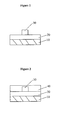
- the optical waveguide assembly comprises a substrate 10, a lower clad layer 20 comprising a cured polymer composition covering a surface of the substrate 10, a silicone core 30 covering a portion of the lower clad layer 20, wherein the silicone core 30 has a refractive index of from 1.30 to 1.65 at 23 °C for light having a wavelength of 589 nm, and the lower clad layer 20 has a refractive index less than the refractive index of the silicone core 30.
- the optical waveguide assembly comprises a substrate 10, a lower clad layer 20 comprising a cured polymer composition covering a surface of the substrate 10, a silicone core 30 covering a portion of the lower clad layer 20, wherein the silicone core 30 has a refractive index of from 1.30 to 1.65 at 23 °C for light having a wavelength of 589 nm, an upper clad layer 40 comprising a second cured polymer composition covering the lower clad layer 20 and the silicone core 30, wherein the lower clad layer 20 and the upper clad layer 40 each have a refractive index less than the refractive index of the silicone core 30.
- the method of the present invention is scaleable to a high throughput manufacturing process.
- the method allows simultaneous fabrication of multiple waveguides on a single substrate.
- the method employs conventional wafer fabrication techniques (e.g., coating, exposing, developing, curing) and equipment.
- the method uses a photopatternable silicone composition, thereby eliminating additional process steps, for example, applying a photoresist and etching, associated with use of a non-photopatternable polymer composition.
- the process of the instant invention has high resolution, meaning that the process transfers images from a photomask to the silicone film on a substrate with good retention of critical dimensions.
- planar optical waveguide assembly of the present invention exhibits good thermal stability over a wide range of temperatures and good environmental resistance, particularly moisture resistance. Also, the waveguide assembly exhibits low birefringence and low transmission loss.
- the optical waveguide assembly of the present invention can be used to fabricate components of optical integrated circuits, such as attenuators, switches, splitters, routers, filters, and gratings.
- Irradiation of a silicone film was carried out using a OAI 7-inch medium pressure mercury projection lamp equipped with a 4-inch diameter interference filter centered at 365 nm (I-line) and having a full width at half maximum (FWHM) of 10 ⁇ 2 nm (Optics Automation Instrumentation, Milpitas, CA). Radiation dose (mJ/cm 2 ) was measured using an International Light radiometer calibrated against I-line radiation.
- Thickness of a cured silicone film on a silicon wafer was determined using a Tencor P-11 surface profilometer (KLA Tencor, Milpitas, CA). Film thickness was measured at a step between the coated and uncoated surfaces of the wafer. The reported value for thickness, in microns, represents the average of three measurements performed on different regions of the same wafer.
- Resolution of the photopatterning process was determined by measuring the size of a feature in the silicone film corresponding to a 250-micron circular aperture (Examples 1-3) or a 40-micron circular aperture (Examples 4-33) in the photomask. Measurements were performed on a digitized photomicrograph of the via using Image Pro Plus image analysis software (Silver Spring, MD). The reported value for resolution, expressed in units of microns, represents the average of four measurements performed on different features of the same wafer.
- Crosslinking Agent A a mixture consisting of 88% of a trimethylsiloxy-tenninated poly(dimethylsiloxane/methylhydrogensiloxane) having an average of 92 dimethylsiloxane units and 6 methylhydrogensiloxane units and per molecule and containing about 0.08 % of silicon-bonded hydrogen atoms; 4% of dimethyl methylhydrogen cyclosiloxane; 4% of octamethylcyclotetrasiloxane; 3% of decamethylcyclopentasiloxane; and 1% of dimethylcyclosiloxanes (D 6 or greater).
- Crosslinking Agent B an organohydrogenpolysiloxane resin consisting essentially of PhSiO 3/2 units and H(CH 3 ) 2 SiO 1/2 units, wherein the mole ratio of PhSiO 3/2 units to H(CH 3 ) 2 SiO 1/2 units is about 1.2, and the resin has a viscosity of about 0.35 Pa ⁇ s, has a weight-average molecular weight of about 1250, and contains about 0.41 wt% of silicon-bonded hydrogen atoms.
- Silicone Base a mixture consisting of 61.32% of Resin A; 22.09% of a mixture consisting of 88% of a trimethylsiloxy-terminated poly(dimethylsiloxane/ methylhydrogensiloxane) having an average of 100 dimethylsiloxane units and 9 methylhydrogensiloxane units per molecule and containing about 0.11% of silicon-bonded hydrogen atoms, 5% of dimethyl methylhydrogen cyclosiloxane, 3% of octamethylcyclotetrasiloxane, 2% of decamethylpentasiloxane, 1% of methylhydrogen cyclosiloxanes, and 0.8% of dimethylcyclosiloxanes (D 6 or greater); 2.33% of a trimethylsiloxy-terminated poly(dimethylsiloxane/methylhydrogensiloxane) having an average of 3 dimethylsiloxane units and 5 methylhydrogensiloxane units per molecule
- the platinum(II) acetylacetonate used to prepare Catalysts A-E was obtained from Strem Chemicals (Newburyport, MA). The material was purified by sublimation at a temperature of 140 °C and a pressure of 4 mmHg.
- Resin A 46.84 parts
- 42.16 parts of Crosslinking Agent A 42.16 parts
- 10.12 parts of mesitylene were combined in an amber bottle.
- Catalyst D (0.89 part) was added to the blend and mixing was continued for 0.5 h at room temperature.
- the mixture was then pressure-filtered (138 to 276 kPa nitrogen) through a stainless steel canister containing 10- ⁇ m and 5- ⁇ lm nylon membranes in series.
- the silicone composition (filtrate) was stored prior to use at -15 °C in a closed polyethylene bottle wrapped in aluminum foil.
- the silicone composition (about 2.5 g), which was at room temperature, was applied to a 100-mm silicon wafer and spun out into a thin film (500 rpm for 10 s followed by 3000 rpm for 30 s).
- the coated wafer was heated on a hot plate at 110 °C for 2 min to remove most of the solvent.
- the film was then exposed to I-line radiation (365 nm) through a photomask containing 250- ⁇ m circular apertures and in near contact with the film.
- the wafer was then heated on a hot plate under the conditions of temperature and time specified in Table 1.
- the wafer was allowed to cool to room temperature and mounted on a spin coater.
- a silicone composition was prepared by combining the a silicone base with the Catalyst specified in Table 2 according to the following procedure: Silicone Base (99.15 parts) and 0.85 part of Catalyst were combined in an amber bottle and mixed for 0.5 h at room temperature. The mixture was then pressure-filtered (138 to 276 kPa nitrogen) through a stainless steel canister containing 10 ⁇ m and 5- ⁇ m nylon membranes in series. The silicone composition (filtrate) was stored prior to use at -15 °C in a closed polyethylene bottle wrapped in aluminum foil.
- Example 4-33 a sample of the silicone composition (about 2.5 g), which was at temperature, was applied to a 100-mm silicon wafer and spun out into a thin film (500 rpm for 10 s followed by 3000 rpm for 30 s). The coated wafer was heated on a hot plate at 110 °C for 2 min to remove most of the solvent. The film was then exposed to I-line radiation (365 nm) through a photomask containing 40- ⁇ m circular apertures and in near contact with the film. The wafer was then heated on a hot plate under the conditions of temperature and time specified in Table 2. The wafer was allowed to cool to room temperature and mounted on a spin coater.
- the coated surface of the wafer was flooded with n-butyl ether and allowed to stand at room temperature for 2 min.
- the wafer was then spun dry (500 rpm for 10 s followed by 3000 rpm for 30 s), placed in an oven for 30 min at 250 °C, and allowed to cool to room temperature.
- the film thickness, film retention, and resolution values for each wafer are reported in Table 2.
- Table 2 Example Catalyst Dose (mJ/cm 2 ) Post. UV Bake Film Thickness ( ⁇ m) Film Retention (%) Resolution ( ⁇ m) Temp.
- Resin B 60.21 parts
- 29.79 parts of Crosslinking Agent B 29.79 parts
- mesitylene 9.00 parts
- Catalyst D (1.00 part) was added to the blend and mixing was continued for 0.5 h at room temperature.
- the mixture was then pressure-filtered (138 to 276 kPa nitrogen) through a stainless steel canister containing 10- ⁇ m and 5- ⁇ m nylon membranes in series.
- the silicone composition (filtrate) was stored prior to use at -15 °C in a closed polyethylene bottle wrapped in aluminum foil.
- Example 34 the silicone composition (about 2.5 g), which was at room temperature, was applied to a 100-mm silicon wafer and spun out into a thin film.
- the wafers were spun at 500 rpm for 10 s (Examples 34 and 36-38) or 25 s (Example 35), followed by 1500 rpm for 20 s.
- the coated wafer was heated on a hot plate at 100 °C for 2 min to remove most of the solvent.
- the film was then exposed to I-line radiation (365 nm) through a photomask containing 250- ⁇ m circular apertures and in near contact with the film.
- the wafer was then heated on a hot plate under the conditions of temperature and time specified in Table 3.
- the wafer was allowed to cool to room temperature and mounted on a spin coater.
- the coated surface of the wafer was flooded with n-butyl ether and allowed to stand at room temperature for 1 min (Examples 34 and 35) or 0.1 min (Examples 36-38).
- the wafer was then spun dry (200 rpm for 30 s followed by 3000 rpm for 30 s), placed in an oven for 30 min at 200 °C, and allowed to cool to room temperature.
- the film thickness, film retention, and resolution values for each wafer are reported in Table 3.
- Table 3 Example Catalyst Dose (mJ/cm 2 ) Post. UV Bake Film Thickness ( ⁇ m) Film Retention (%) Resolution ( ⁇ m) Temp.
Landscapes
- Physics & Mathematics (AREA)
- General Physics & Mathematics (AREA)
- Engineering & Computer Science (AREA)
- Optics & Photonics (AREA)
- Microelectronics & Electronic Packaging (AREA)
- Chemical & Material Sciences (AREA)
- Life Sciences & Earth Sciences (AREA)
- Spectroscopy & Molecular Physics (AREA)
- Chemical Kinetics & Catalysis (AREA)
- General Chemical & Material Sciences (AREA)
- Geochemistry & Mineralogy (AREA)
- Materials Engineering (AREA)
- Organic Chemistry (AREA)
- Compositions Of Macromolecular Compounds (AREA)
- Optical Integrated Circuits (AREA)
Applications Claiming Priority (3)
| Application Number | Priority Date | Filing Date | Title |
|---|---|---|---|
| US179096 | 1988-04-08 | ||
| US10/179,096 US6905904B2 (en) | 2002-06-24 | 2002-06-24 | Planar optical waveguide assembly and method of preparing same |
| PCT/US2003/009699 WO2004001458A1 (en) | 2002-06-24 | 2003-03-28 | Planar optical waveguide assembly and method of preparing same |
Publications (2)
| Publication Number | Publication Date |
|---|---|
| EP1516208A1 EP1516208A1 (en) | 2005-03-23 |
| EP1516208B1 true EP1516208B1 (en) | 2014-11-05 |
Family
ID=29734855
Family Applications (1)
| Application Number | Title | Priority Date | Filing Date |
|---|---|---|---|
| EP03719514.6A Expired - Lifetime EP1516208B1 (en) | 2002-06-24 | 2003-03-28 | Planar optical waveguide assembly and method of preparing same |
Country Status (5)
| Country | Link |
|---|---|
| US (2) | US6905904B2 (enExample) |
| EP (1) | EP1516208B1 (enExample) |
| JP (1) | JP4849799B2 (enExample) |
| AU (1) | AU2003223392A1 (enExample) |
| WO (1) | WO2004001458A1 (enExample) |
Cited By (1)
| Publication number | Priority date | Publication date | Assignee | Title |
|---|---|---|---|---|
| CN104610752B (zh) * | 2013-11-05 | 2019-05-28 | 信越化学工业株式会社 | Uv固化性粘合性有机聚硅氧烷组合物 |
Families Citing this family (44)
| Publication number | Priority date | Publication date | Assignee | Title |
|---|---|---|---|---|
| US20100273011A1 (en) * | 1996-12-20 | 2010-10-28 | Bianxiao Zhong | Silicone Composition, Silicone Adhesive, Coated and Laminated Substrates |
| US6907176B2 (en) * | 2002-06-24 | 2005-06-14 | Dow Corning Corporation | Planar optical waveguide assembly and method of preparing same |
| US6768828B2 (en) * | 2002-11-04 | 2004-07-27 | Little Optics Inc. | Integrated optical circuit with dense planarized cladding layer |
| TWI285664B (en) * | 2003-12-25 | 2007-08-21 | Kansai Paint Co Ltd | Curable resin composition for optical waveguide, curable dry film for optical waveguide, waveguide, and, method for manufacturing optical waveguide |
| WO2006001447A1 (ja) * | 2004-06-28 | 2006-01-05 | Omron Corporation | フィルム光導波路及びその製造方法並びに電子機器装置 |
| WO2006023037A2 (en) * | 2004-08-11 | 2006-03-02 | Dow Corning Corporation | Photopolymerizable silicone materials forming semipermeable membranes for sensor applications |
| JP4800383B2 (ja) * | 2005-05-26 | 2011-10-26 | ダウ・コーニング・コーポレイション | 小さい形状を成形するための方法およびシリコーン封止剤組成物 |
| MY144041A (en) * | 2006-01-17 | 2011-07-29 | Dow Corning | Thermally stable transparent silicone resin compositions and methods for their preparation and use |
| CN101336383B (zh) * | 2006-02-01 | 2012-05-09 | 陶氏康宁公司 | 抗冲击的光波导管及其制造方法 |
| CN101389695B (zh) * | 2006-02-24 | 2012-07-04 | 陶氏康宁公司 | 用硅氧烷包封的发光器件和用于制备该硅氧烷的可固化的硅氧烷组合物 |
| EP2075310B1 (en) * | 2006-08-31 | 2012-03-14 | Nippon Steel Chemical Co., Ltd. | Organic electroluminescent device material and organic electroluminescent device |
| WO2008088407A1 (en) * | 2006-12-20 | 2008-07-24 | Dow Corning Corporation | Glass substrates coated or laminated with multiple layers of cured silicone resin compositions |
| JP5357046B2 (ja) * | 2006-12-20 | 2013-12-04 | ダウ・コーニング・コーポレイション | 硬化シリコーン組成物で被覆またはラミネートされたガラス基板 |
| KR101533470B1 (ko) * | 2007-09-19 | 2015-07-02 | 히타치가세이가부시끼가이샤 | 광도파로의 제조방법 및 그 제조방법에 의해 얻어진 광도파로 |
| US7944781B2 (en) * | 2007-10-16 | 2011-05-17 | Seagate Technology Llc | Flexible waveguide with adjustable index of refraction |
| WO2009111193A1 (en) * | 2008-03-04 | 2009-09-11 | Dow Corning Corporation | Borosiloxane composition, borosiloxane adhesive, coated and laminated substrates |
| WO2009111199A1 (en) * | 2008-03-04 | 2009-09-11 | Dow Corning Corporation | Silicone composition, silicone adhesive, coated and laminated substrates |
| WO2009146254A1 (en) * | 2008-05-27 | 2009-12-03 | Dow Corning Corporation | Adhesive tape and laminated glass |
| TW201004795A (en) * | 2008-07-31 | 2010-02-01 | Dow Corning | Laminated glass |
| JP5100681B2 (ja) * | 2009-02-16 | 2012-12-19 | 富士フイルム株式会社 | 微細パターン形成用部材 |
| US9080077B2 (en) | 2009-12-21 | 2015-07-14 | Dow Corning Corporation | Methods for fabricating flexible waveguides using alkyl-functional silsesquioxane resins |
| DE102010043149A1 (de) * | 2010-10-29 | 2012-05-03 | Wacker Chemie Ag | Hochtransparente durch Licht vernetzbare Siliconmischungen |
| US9012547B2 (en) | 2010-11-09 | 2015-04-21 | Dow Corning Corporation | Hydrosilylation cured silicone resins plasticized by organophosphorous compounds |
| JP5490671B2 (ja) * | 2010-12-07 | 2014-05-14 | 信越化学工業株式会社 | シリコーン樹脂組成物の硬化方法 |
| US9354518B2 (en) | 2011-05-25 | 2016-05-31 | Dow Corning Corporation | Epoxy-functional radiation-curable composition containing an epoxy-functional siloxane oligomer for enhanced film retention and adhesion during solvent development |
| JP5472241B2 (ja) * | 2011-09-16 | 2014-04-16 | 信越化学工業株式会社 | 光硬化型シリコーン樹脂組成物を用いる硬化薄膜の製造方法 |
| JP2016526069A (ja) | 2013-05-17 | 2016-09-01 | ダウ コーニング コーポレーションDow Corning Corporation | 硬化性組成物、硬化された物品の調製方法、及び該方法により形成された硬化物品 |
| WO2014186549A1 (en) * | 2013-05-17 | 2014-11-20 | Dow Corning Corporation | Method of preparing an article and article prepared thereby |
| US11320267B2 (en) | 2017-03-23 | 2022-05-03 | Kvh Industries, Inc. | Integrated optic wavemeter and method for fiber optic gyroscopes scale factor stabilization |
| US20200278611A1 (en) * | 2017-07-28 | 2020-09-03 | Dow Silicones Corporation | A method of preparing a planar optical waveguide assembly |
| US10852480B2 (en) * | 2017-08-24 | 2020-12-01 | Dow Global Technologies Llc | Method for optical waveguide fabrication using polysiloxane, epoxy, photo acid generator, and hydrosilation catalyst |
| KR102620913B1 (ko) * | 2017-08-24 | 2024-01-05 | 다우 글로벌 테크놀로지스 엘엘씨 | 광학 도파관 제작 방법 |
| EP3673307B1 (en) * | 2017-08-24 | 2021-08-25 | Dow Global Technologies LLC | Method for optical waveguide fabrication |
| KR20200060718A (ko) | 2017-09-15 | 2020-06-01 | 케이브이에이치 인더스트리즈, 인코포레이티드 | 광자 집적 회로의 도파관에 광섬유의 자기 정렬 연결을 위한 방법 및 장치 |
| WO2019209395A1 (en) * | 2018-04-24 | 2019-10-31 | Dow Silicones Corporation | Positive tone photopatternable silicone |
| KR20210084492A (ko) | 2018-10-11 | 2021-07-07 | 케이브이에이치 인더스트리즈, 인코포레이티드 | 광 집적 회로, 섬유광 자이로스코프, 및 그 제조 방법 |
| CA3115836A1 (en) | 2018-10-31 | 2020-05-07 | Kvh Industries, Inc. | Method and apparatus for control and suppression of stray light in a photonic integrated circuit |
| US11353655B2 (en) * | 2019-05-22 | 2022-06-07 | Kvh Industries, Inc. | Integrated optical polarizer and method of making same |
| CN115003760A (zh) * | 2019-12-26 | 2022-09-02 | 陶氏东丽株式会社 | 固化性聚有机硅氧烷组合物和其固化物、保护剂或粘接剂以及电气/电子设备 |
| GB202108979D0 (en) | 2021-06-23 | 2021-08-04 | Johnson Matthey Plc | Hydrosilylation catalysts |
| ES1281409Y (es) | 2021-07-29 | 2022-02-01 | Univ Valencia Politecnica | Dispositivo de ahorro de agua para instalaciones de agua caliente sanitaria |
| US12352571B2 (en) | 2021-08-11 | 2025-07-08 | Emcore Corporation | In-situ residual intensity noise measurement method and system |
| WO2023211518A2 (en) | 2021-11-30 | 2023-11-02 | Emcore Corporation | Multi-axis fiber optic gyroscope photonic integrated circuit for inertial measurement units and inertial navigation systems |
| TW202428780A (zh) | 2022-12-05 | 2024-07-16 | 美商陶氏有機矽公司 | Uv可固化聚矽氧組成物 |
Family Cites Families (33)
| Publication number | Priority date | Publication date | Assignee | Title |
|---|---|---|---|---|
| US3934061A (en) * | 1972-03-30 | 1976-01-20 | Corning Glass Works | Method of forming planar optical waveguides |
| ES8403555A1 (es) | 1983-03-08 | 1984-03-16 | Zottnik Edmund | Sistema codificado de validacion y comando. |
| US5080962A (en) * | 1985-02-25 | 1992-01-14 | University Of Florida | Method for making silica optical devices and devices produced thereby |
| JPS61275706A (ja) * | 1985-05-30 | 1986-12-05 | Sumitomo Electric Ind Ltd | 光導波路 |
| JPS6239660A (ja) * | 1985-08-14 | 1987-02-20 | Toshiba Silicone Co Ltd | 光学的接合用ゲル組成物 |
| FR2597110A1 (fr) | 1986-04-14 | 1987-10-16 | Rhone Poulenc Multi Tech | Composition organopolysiloxane, potentiellement reticulable et utilisable notamment en microlithographie, et son procede d'application |
| JPS63273804A (ja) * | 1987-05-01 | 1988-11-10 | Sumitomo Electric Ind Ltd | 光導波路 |
| JPS6457207A (en) * | 1987-08-28 | 1989-03-03 | Hitachi Ltd | Waveguide type optical device |
| JPS6459302A (en) * | 1987-08-31 | 1989-03-07 | Sumitomo Electric Industries | Manufacturer of plastic optical waveguide sheet |
| JP3273519B2 (ja) * | 1992-12-04 | 2002-04-08 | 日本電信電話株式会社 | ポリシロキサン系光導波路の製造方法 |
| JPH07140336A (ja) * | 1993-09-22 | 1995-06-02 | Shin Etsu Chem Co Ltd | 光導波路 |
| JPH0862440A (ja) * | 1994-08-17 | 1996-03-08 | Nippon Telegr & Teleph Corp <Ntt> | 光導波路及びその作製方法 |
| JPH07331173A (ja) * | 1995-02-21 | 1995-12-19 | Toray Ind Inc | 光学材料形成用塗液組成物および光学材料 |
| JPH07258604A (ja) * | 1995-02-21 | 1995-10-09 | Toray Ind Inc | 光学材料および光学材料用コーティング組成物 |
| JPH09124793A (ja) | 1995-11-02 | 1997-05-13 | Nippon Telegr & Teleph Corp <Ntt> | 高分子光学材料及びその製造方法及び高分子光導波路 |
| US5972516A (en) * | 1996-02-29 | 1999-10-26 | Kyocera Corporation | Method for manufacturing optical waveguide using siloxane polymer, and optoelectronic hybrid substrate using the optical waveguide |
| JPH1067935A (ja) * | 1996-08-29 | 1998-03-10 | Toray Dow Corning Silicone Co Ltd | 硬化性オルガノポリシロキサン組成物 |
| DE19645721A1 (de) * | 1996-11-06 | 1998-05-07 | Wacker Chemie Gmbh | Vernetzbare Organopolysiloxanmassen |
| JPH10148729A (ja) | 1996-11-21 | 1998-06-02 | Nippon Telegr & Teleph Corp <Ntt> | 高分子光導波路コア部のリッジ・パターン形成方法 |
| US6054253A (en) * | 1997-10-10 | 2000-04-25 | Mcgill University-The Royal Institute For The Advancement Of Learning | Solvent-assisted lithographic process using photosensitive sol-gel derived glass for depositing ridge waveguides on silicon |
| JP3063903B2 (ja) * | 1998-03-20 | 2000-07-12 | 日本電信電話株式会社 | 光導波路 |
| US6482551B1 (en) * | 1998-03-24 | 2002-11-19 | Inphase Technologies | Optical article and process for forming article |
| JP2000090643A (ja) | 1998-09-08 | 2000-03-31 | Matsushita Electric Ind Co Ltd | 記憶装置 |
| JP3133039B2 (ja) * | 1998-10-05 | 2001-02-05 | 日本電信電話株式会社 | 光導波路用感光性組成物およびその製造方法および高分子光導波路パターン形成方法 |
| JP4362255B2 (ja) * | 1999-09-16 | 2009-11-11 | 日本板硝子株式会社 | 所定表面形状を有する物品の製造方法および光導波路素子 |
| WO2001037049A1 (en) * | 1999-11-12 | 2001-05-25 | Nippon Sheet Glass Co., Ltd. | Photosensitive composition, and optical waveguide element and process for producing the same |
| JP2001288364A (ja) * | 2000-04-05 | 2001-10-16 | Jsr Corp | 放射線硬化性組成物およびそれを用いた光導波路ならびに光導波路の製造方法 |
| JP2001318248A (ja) * | 2000-05-12 | 2001-11-16 | Mitsubishi Electric Corp | 高分子光導波路の製造方法 |
| US6415093B1 (en) * | 2000-08-17 | 2002-07-02 | Nippon Sheet Glass Co., Ltd. | Optical device and adhesive composition used therefor |
| US6991887B1 (en) * | 2000-11-01 | 2006-01-31 | Battelle Memorial Institute | Photopatternable sorbent and functionalized films |
| US6617674B2 (en) | 2001-02-20 | 2003-09-09 | Dow Corning Corporation | Semiconductor package and method of preparing same |
| JP2003131058A (ja) * | 2001-08-09 | 2003-05-08 | Kanegafuchi Chem Ind Co Ltd | 光導波路および光導波路の作製方法。 |
| JP2004012635A (ja) * | 2002-06-04 | 2004-01-15 | Nippon Paint Co Ltd | 光電気配線複合実装基板及びその製造方法 |
-
2002
- 2002-06-24 US US10/179,096 patent/US6905904B2/en not_active Expired - Lifetime
-
2003
- 2003-03-28 EP EP03719514.6A patent/EP1516208B1/en not_active Expired - Lifetime
- 2003-03-28 WO PCT/US2003/009699 patent/WO2004001458A1/en not_active Ceased
- 2003-03-28 AU AU2003223392A patent/AU2003223392A1/en not_active Abandoned
- 2003-03-28 JP JP2004515621A patent/JP4849799B2/ja not_active Expired - Fee Related
-
2005
- 2005-04-13 US US11/104,814 patent/US7358582B2/en not_active Expired - Lifetime
Cited By (1)
| Publication number | Priority date | Publication date | Assignee | Title |
|---|---|---|---|---|
| CN104610752B (zh) * | 2013-11-05 | 2019-05-28 | 信越化学工业株式会社 | Uv固化性粘合性有机聚硅氧烷组合物 |
Also Published As
| Publication number | Publication date |
|---|---|
| WO2004001458A1 (en) | 2003-12-31 |
| EP1516208A1 (en) | 2005-03-23 |
| JP4849799B2 (ja) | 2012-01-11 |
| US7358582B2 (en) | 2008-04-15 |
| US20050175301A1 (en) | 2005-08-11 |
| US20030235383A1 (en) | 2003-12-25 |
| JP2005531029A (ja) | 2005-10-13 |
| AU2003223392A1 (en) | 2004-01-06 |
| US6905904B2 (en) | 2005-06-14 |
Similar Documents
| Publication | Publication Date | Title |
|---|---|---|
| EP1516208B1 (en) | Planar optical waveguide assembly and method of preparing same | |
| EP1523525B1 (en) | Planar optical waveguide assembly and method of preparing same | |
| JP2005531029A5 (enExample) | ||
| KR890003264B1 (ko) | 3층 레지스트 및 레지스트 패턴의 형성방법 | |
| WO2005017627A1 (en) | Method for etching a patterned silicone layyer | |
| JP5975582B2 (ja) | エポキシ官能性シロキサンオリゴマーを含有するエポキシ官能性の放射線硬化性組成物 | |
| KR101135375B1 (ko) | 센서용 반투과성 막을 형성하는 광중합 가능한 실리콘 재료 | |
| US7517808B2 (en) | Method for forming and removing a patterned silicone film | |
| US8227181B2 (en) | Method of preparing a patterned film with a developing solvent | |
| US20200278611A1 (en) | A method of preparing a planar optical waveguide assembly | |
| EP0199940B1 (en) | Photolithographic process, and organosilicone polymer composition for use therein | |
| Shanmugam et al. | Silica-like microstructures by x-ray irradiation of polymethylsilsesquioxane spin-on glass films |
Legal Events
| Date | Code | Title | Description |
|---|---|---|---|
| PUAI | Public reference made under article 153(3) epc to a published international application that has entered the european phase |
Free format text: ORIGINAL CODE: 0009012 |
|
| 17P | Request for examination filed |
Effective date: 20041224 |
|
| AK | Designated contracting states |
Kind code of ref document: A1 Designated state(s): AT BE BG CH CY CZ DE DK EE ES FI FR GB GR HU IE IT LI LU MC NL PT RO SE SI SK TR |
|
| AX | Request for extension of the european patent |
Extension state: AL LT LV MK |
|
| DAX | Request for extension of the european patent (deleted) | ||
| RIN1 | Information on inventor provided before grant (corrected) |
Inventor name: GARDNER, GEOFFREY Inventor name: SCHMIDT, RANDALL |
|
| 17Q | First examination report despatched |
Effective date: 20070810 |
|
| GRAP | Despatch of communication of intention to grant a patent |
Free format text: ORIGINAL CODE: EPIDOSNIGR1 |
|
| RIC1 | Information provided on ipc code assigned before grant |
Ipc: G03F 7/075 20060101ALI20140516BHEP Ipc: G02B 6/132 20060101ALI20140516BHEP Ipc: C03C 17/34 20060101ALI20140516BHEP Ipc: C08L 83/04 20060101ALI20140516BHEP Ipc: G03F 7/00 20060101ALI20140516BHEP Ipc: G02B 1/04 20060101AFI20140516BHEP Ipc: G02B 6/138 20060101ALI20140516BHEP Ipc: G02B 6/12 20060101ALI20140516BHEP |
|
| INTG | Intention to grant announced |
Effective date: 20140611 |
|
| GRAS | Grant fee paid |
Free format text: ORIGINAL CODE: EPIDOSNIGR3 |
|
| GRAA | (expected) grant |
Free format text: ORIGINAL CODE: 0009210 |
|
| AK | Designated contracting states |
Kind code of ref document: B1 Designated state(s): AT BE BG CH CY CZ DE DK EE ES FI FR GB GR HU IE IT LI LU MC NL PT RO SE SI SK TR |
|
| REG | Reference to a national code |
Ref country code: GB Ref legal event code: FG4D |
|
| REG | Reference to a national code |
Ref country code: CH Ref legal event code: EP |
|
| REG | Reference to a national code |
Ref country code: AT Ref legal event code: REF Ref document number: 694906 Country of ref document: AT Kind code of ref document: T Effective date: 20141115 |
|
| REG | Reference to a national code |
Ref country code: IE Ref legal event code: FG4D |
|
| REG | Reference to a national code |
Ref country code: DE Ref legal event code: R096 Ref document number: 60346951 Country of ref document: DE Effective date: 20141211 |
|
| REG | Reference to a national code |
Ref country code: AT Ref legal event code: MK05 Ref document number: 694906 Country of ref document: AT Kind code of ref document: T Effective date: 20141105 |
|
| REG | Reference to a national code |
Ref country code: NL Ref legal event code: VDEP Effective date: 20141105 |
|
| PG25 | Lapsed in a contracting state [announced via postgrant information from national office to epo] |
Ref country code: FI Free format text: LAPSE BECAUSE OF FAILURE TO SUBMIT A TRANSLATION OF THE DESCRIPTION OR TO PAY THE FEE WITHIN THE PRESCRIBED TIME-LIMIT Effective date: 20141105 Ref country code: ES Free format text: LAPSE BECAUSE OF FAILURE TO SUBMIT A TRANSLATION OF THE DESCRIPTION OR TO PAY THE FEE WITHIN THE PRESCRIBED TIME-LIMIT Effective date: 20141105 Ref country code: PT Free format text: LAPSE BECAUSE OF FAILURE TO SUBMIT A TRANSLATION OF THE DESCRIPTION OR TO PAY THE FEE WITHIN THE PRESCRIBED TIME-LIMIT Effective date: 20150305 Ref country code: NL Free format text: LAPSE BECAUSE OF FAILURE TO SUBMIT A TRANSLATION OF THE DESCRIPTION OR TO PAY THE FEE WITHIN THE PRESCRIBED TIME-LIMIT Effective date: 20141105 |
|
| PG25 | Lapsed in a contracting state [announced via postgrant information from national office to epo] |
Ref country code: GR Free format text: LAPSE BECAUSE OF FAILURE TO SUBMIT A TRANSLATION OF THE DESCRIPTION OR TO PAY THE FEE WITHIN THE PRESCRIBED TIME-LIMIT Effective date: 20150206 Ref country code: CY Free format text: LAPSE BECAUSE OF FAILURE TO SUBMIT A TRANSLATION OF THE DESCRIPTION OR TO PAY THE FEE WITHIN THE PRESCRIBED TIME-LIMIT Effective date: 20141105 Ref country code: SE Free format text: LAPSE BECAUSE OF FAILURE TO SUBMIT A TRANSLATION OF THE DESCRIPTION OR TO PAY THE FEE WITHIN THE PRESCRIBED TIME-LIMIT Effective date: 20141105 Ref country code: AT Free format text: LAPSE BECAUSE OF FAILURE TO SUBMIT A TRANSLATION OF THE DESCRIPTION OR TO PAY THE FEE WITHIN THE PRESCRIBED TIME-LIMIT Effective date: 20141105 |
|
| PG25 | Lapsed in a contracting state [announced via postgrant information from national office to epo] |
Ref country code: RO Free format text: LAPSE BECAUSE OF FAILURE TO SUBMIT A TRANSLATION OF THE DESCRIPTION OR TO PAY THE FEE WITHIN THE PRESCRIBED TIME-LIMIT Effective date: 20141105 Ref country code: SK Free format text: LAPSE BECAUSE OF FAILURE TO SUBMIT A TRANSLATION OF THE DESCRIPTION OR TO PAY THE FEE WITHIN THE PRESCRIBED TIME-LIMIT Effective date: 20141105 Ref country code: EE Free format text: LAPSE BECAUSE OF FAILURE TO SUBMIT A TRANSLATION OF THE DESCRIPTION OR TO PAY THE FEE WITHIN THE PRESCRIBED TIME-LIMIT Effective date: 20141105 Ref country code: CZ Free format text: LAPSE BECAUSE OF FAILURE TO SUBMIT A TRANSLATION OF THE DESCRIPTION OR TO PAY THE FEE WITHIN THE PRESCRIBED TIME-LIMIT Effective date: 20141105 Ref country code: DK Free format text: LAPSE BECAUSE OF FAILURE TO SUBMIT A TRANSLATION OF THE DESCRIPTION OR TO PAY THE FEE WITHIN THE PRESCRIBED TIME-LIMIT Effective date: 20141105 |
|
| REG | Reference to a national code |
Ref country code: DE Ref legal event code: R097 Ref document number: 60346951 Country of ref document: DE |
|
| PLBE | No opposition filed within time limit |
Free format text: ORIGINAL CODE: 0009261 |
|
| STAA | Information on the status of an ep patent application or granted ep patent |
Free format text: STATUS: NO OPPOSITION FILED WITHIN TIME LIMIT |
|
| 26N | No opposition filed |
Effective date: 20150806 |
|
| PG25 | Lapsed in a contracting state [announced via postgrant information from national office to epo] |
Ref country code: LU Free format text: LAPSE BECAUSE OF FAILURE TO SUBMIT A TRANSLATION OF THE DESCRIPTION OR TO PAY THE FEE WITHIN THE PRESCRIBED TIME-LIMIT Effective date: 20150328 Ref country code: MC Free format text: LAPSE BECAUSE OF FAILURE TO SUBMIT A TRANSLATION OF THE DESCRIPTION OR TO PAY THE FEE WITHIN THE PRESCRIBED TIME-LIMIT Effective date: 20141105 |
|
| REG | Reference to a national code |
Ref country code: CH Ref legal event code: PL |
|
| GBPC | Gb: european patent ceased through non-payment of renewal fee |
Effective date: 20150328 |
|
| PG25 | Lapsed in a contracting state [announced via postgrant information from national office to epo] |
Ref country code: IT Free format text: LAPSE BECAUSE OF FAILURE TO SUBMIT A TRANSLATION OF THE DESCRIPTION OR TO PAY THE FEE WITHIN THE PRESCRIBED TIME-LIMIT Effective date: 20141105 |
|
| REG | Reference to a national code |
Ref country code: FR Ref legal event code: ST Effective date: 20151130 |
|
| REG | Reference to a national code |
Ref country code: IE Ref legal event code: MM4A |
|
| PG25 | Lapsed in a contracting state [announced via postgrant information from national office to epo] |
Ref country code: CH Free format text: LAPSE BECAUSE OF NON-PAYMENT OF DUE FEES Effective date: 20150331 Ref country code: GB Free format text: LAPSE BECAUSE OF NON-PAYMENT OF DUE FEES Effective date: 20150328 Ref country code: IE Free format text: LAPSE BECAUSE OF NON-PAYMENT OF DUE FEES Effective date: 20150328 Ref country code: LI Free format text: LAPSE BECAUSE OF NON-PAYMENT OF DUE FEES Effective date: 20150331 |
|
| PG25 | Lapsed in a contracting state [announced via postgrant information from national office to epo] |
Ref country code: FR Free format text: LAPSE BECAUSE OF NON-PAYMENT OF DUE FEES Effective date: 20150331 Ref country code: SI Free format text: LAPSE BECAUSE OF FAILURE TO SUBMIT A TRANSLATION OF THE DESCRIPTION OR TO PAY THE FEE WITHIN THE PRESCRIBED TIME-LIMIT Effective date: 20141105 |
|
| PG25 | Lapsed in a contracting state [announced via postgrant information from national office to epo] |
Ref country code: HU Free format text: LAPSE BECAUSE OF FAILURE TO SUBMIT A TRANSLATION OF THE DESCRIPTION OR TO PAY THE FEE WITHIN THE PRESCRIBED TIME-LIMIT; INVALID AB INITIO Effective date: 20030328 Ref country code: BG Free format text: LAPSE BECAUSE OF FAILURE TO SUBMIT A TRANSLATION OF THE DESCRIPTION OR TO PAY THE FEE WITHIN THE PRESCRIBED TIME-LIMIT Effective date: 20141105 |
|
| PG25 | Lapsed in a contracting state [announced via postgrant information from national office to epo] |
Ref country code: TR Free format text: LAPSE BECAUSE OF FAILURE TO SUBMIT A TRANSLATION OF THE DESCRIPTION OR TO PAY THE FEE WITHIN THE PRESCRIBED TIME-LIMIT Effective date: 20141105 |
|
| PG25 | Lapsed in a contracting state [announced via postgrant information from national office to epo] |
Ref country code: BE Free format text: LAPSE BECAUSE OF FAILURE TO SUBMIT A TRANSLATION OF THE DESCRIPTION OR TO PAY THE FEE WITHIN THE PRESCRIBED TIME-LIMIT Effective date: 20141105 |
|
| PGFP | Annual fee paid to national office [announced via postgrant information from national office to epo] |
Ref country code: DE Payment date: 20220203 Year of fee payment: 20 |
|
| REG | Reference to a national code |
Ref country code: DE Ref legal event code: R071 Ref document number: 60346951 Country of ref document: DE |