EP1513157A1 - Method for multibank memory scheduling - Google Patents
Method for multibank memory scheduling Download PDFInfo
- Publication number
- EP1513157A1 EP1513157A1 EP03019948A EP03019948A EP1513157A1 EP 1513157 A1 EP1513157 A1 EP 1513157A1 EP 03019948 A EP03019948 A EP 03019948A EP 03019948 A EP03019948 A EP 03019948A EP 1513157 A1 EP1513157 A1 EP 1513157A1
- Authority
- EP
- European Patent Office
- Prior art keywords
- bank
- input stream
- writing
- banks
- stream
- Prior art date
- Legal status (The legal status is an assumption and is not a legal conclusion. Google has not performed a legal analysis and makes no representation as to the accuracy of the status listed.)
- Withdrawn
Links
Images


Classifications
-
- G—PHYSICS
- G06—COMPUTING; CALCULATING OR COUNTING
- G06F—ELECTRIC DIGITAL DATA PROCESSING
- G06F12/00—Accessing, addressing or allocating within memory systems or architectures
- G06F12/02—Addressing or allocation; Relocation
-
- G—PHYSICS
- G11—INFORMATION STORAGE
- G11C—STATIC STORES
- G11C7/00—Arrangements for writing information into, or reading information out from, a digital store
- G11C7/10—Input/output [I/O] data interface arrangements, e.g. I/O data control circuits, I/O data buffers
- G11C7/1015—Read-write modes for single port memories, i.e. having either a random port or a serial port
- G11C7/1042—Read-write modes for single port memories, i.e. having either a random port or a serial port using interleaving techniques, i.e. read-write of one part of the memory while preparing another part
-
- G—PHYSICS
- G06—COMPUTING; CALCULATING OR COUNTING
- G06F—ELECTRIC DIGITAL DATA PROCESSING
- G06F12/00—Accessing, addressing or allocating within memory systems or architectures
- G06F12/02—Addressing or allocation; Relocation
- G06F12/06—Addressing a physical block of locations, e.g. base addressing, module addressing, memory dedication
Definitions
- the present invention relates to a method for scheduling and controlling access to a multibank memory, and to an apparatus for reading from and/or writing to recording media using such method.
- SDRAM synchronous dynamical random access memory
- DDR-RAM double data rate RAM
- ESDRAM enhanced synchronous DRAM
- SLDRAM synchronous link DRAM
- RDRAM Rambus DRAM
- the invention is also applicable to single-port static random access memory (single-port SRAM) .
- Typical SDRAM modules comprise four independent banks. Each bank consists of rows, which consist of columns. To access a datum the corresponding row on the corresponding bank is opened by the command 'activate' for reading and writing. After activation, which needs 2 to 4 cycles, the data transfer is initiated by sending a 'read' or 'write' command together with the column address. After the transfer the bank is precharged, which again needs 2 to 4 cycles, to deactivate the open row and to prepare the bank for the next 'activate' command. The command 'precharge' closes the open row.
- a burst transfer is used for reading or writing several data with only one 'read' or 'write' command.
- the access starts at a selected location (column) and continues for a programmed number of locations. After initiating a new burst, the command bus is free and can be used to activate or precharge other banks.
- SDRAM is used for simultaneously storing CPU-instructions as well as data.
- the SDRAM is accessed through a cache.
- a linear access is achieved in the following way: first bank first row, second bank first row, third bank first row, fourth bank first row, first bank second row and so on. Assuming a linear access this allows to hide latency by activating the row on the next bank before the CPU/cache actually wants to access this row.
- a single SDRAM module is favorably used for storing instructions and data for an on-chip-CPU and for buffering the real-time data stream between a drive for the recording media and a host.
- the burst length of the buffer input and output stream need to be reduced to only a few beats.
- the overhead caused by the four interfaces, i.e. CPU-instructions, CPU-data, input stream, and output stream acts like random access.
- read and write access to the buffer is in random order. Therefore, since the next row is unknown, pre-activation of buffer banks is not possible.
- the SDRAM module can be replaced by static RAM (SRAM).
- SRAM static RAM
- the number of modules can be increased for reducing the workload of a single module, or the width of the data bus between the module and the application specific integrated circuit (ASIC) can be expanded for increasing the bandwidth.
- a further solution consists in de-coupling the buffer input and output, which can be performed by large on-chip SRAM buffering two or more complete rows.
- a very complex logic is required for controlling the data flow.
- a method for controlling access to a multibank memory having at least two banks comprises the steps of:
- the method further comprises the steps of:
- the method further comprises the steps of:
- the method further comprises the steps of:
- the multibank memory is a dynamical random access memory, e.g. an SDRAM.
- the method according to the invention takes full advantage of the pipelining architecture of the memory.
- the method further comprises the step of holding an activated row of a bank open until a refresh cycle is issued or until the end of the row is reached by a burst. This allows to save approximately ten cycles latency for each single access.
- the banks are single-port static random access memory modules.
- input data are written into the first module until a read request is received for this module.
- the input data are then written into the second module whilst data are read from the first module. Reading and writing is, therefore, performed simultaneously.
- a further advantage is that instead of a more expensive and complicated dual-port SRAM module of a specific size two single-port SRAM modules with half the size each can be used, e.g. two single-port SRAM modules with 512 bytes each instead of a dual-port SRAM module with 1024 bytes.
- more than two banks are provided for data buffering. This allows to buffer a larger amount of data. However, the overall performance is not further enhanced by this measure.
- the method further comprises the steps of:
- a device for controlling access to a multibank memory having at least two banks performs a method according to the invention.
- an apparatus for reading from and/or writing to recording media uses a method or comprises a device according to the invention for controlling access to a multibank memory having at least two banks.
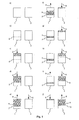
- Fig. 1 access to two banks 1,2 of an SDRAM using a method according to the invention is shown.
- the access is divided into a sequence of states of the banks, which are depicted in parts a) to j) of Fig. 1.
- a single complete output block is written into one bank 1,2.
- a plurality of output blocks can subsequently be written into the banks.
- both banks 1,2 are empty, which corresponds to Fig. 1a).
- a pointer 5 is set to mark the size of an output block.
- the input stream 6 coming from the drive are now stored in the left bank 1, which is depicted in part c). As soon as the pointer 5 is reached, the buffer can be read.
- the writing to the left bank 1 continues. This is shown in part d).
- the first bank 1 is filled with a plurality of output blocks.
- the input stream 6 is switched to the right bank 2 and its last position on the left bank 1 is marked with a further pointer 7, which is depicted in part e).
- the input stream 6 and the output stream 8 are active at the same time until the complete output block size has been read from the left bank 1.
- a new pointer 9 is set marking the size of an output block, which is shown in part h). When this pointer 9 is reached, the left bank 1 is read until the jump point 7 is reached.
- the access scheme can be extended to more than two banks. In this case upon switching between the banks it is possible to choose among at least two banks for writing the imput stream. By way of example, this choice can be based on the overall workload of each bank.
- Latencies during data transfer on an SDRAM bank 1, 2 are shown in Fig. 2.
- the data transfer is divided into data transfer occurring on a command bus 3 and data transfer occurring on a data bus 4.
- Fig. 2a depicts a typical random read/write access to one SDRAM bank only. First a row from that bank is activated. Then a write command to that row is issued and the data transfer is initiated. After that a precharge command is given for closing the row and for precharging for the next row access. Another row on the same bank is then activated, a read command to that row is issued and data transfer starts after a delay due to the 'read' command.
- FIG. 2b An SDRAM access over more than one bank is shown in Fig. 2b).
- First a row from a first bank is activated.
- a write command to that row from the first bank is then issued and data transfer is initiated.
- Simultaneously a row from a second bank is activated.
- a read command to that row from the second bank is then given and data transfer starts after a delay due to the 'read' command. It is to be noted that a write command in this example would lead to a data transfer from the second bank directly concatenated to the data transfer of the first bank.
- Fig. 2c shows a single burst to an already opened row on the same bank. In this case a write command is each time processed without delay on that row.
- FIG. 3 an apparatus for reading from recording media 20, e.g. optical recording media, using a method according to the invention is shown.
- Data are read from the recording medium 20 and are pre-processed by a pre-processing block 21, e.g. for error correction.
- the pre-processed data are transmitted as an input stream via a first interface 23 to an integrated circuit 22, which among other functions controls the data transfer within the apparatus.
- the integrated circuit 22 Via a second interface 24 the integrated circuit 22 communicates with a data bus 28, e.g. an ATA bus. Using this data bus 28 requested data are output for further processing.
- a micro-controller 29 communicates with the integrated circuit 22 via a third interface 25, e.g. for controlling settings of the integrated circuit 22 or for requesting specific data.
- the integrated circuit comprises an internal buffer 26 comprising a plurality of SDRAM banks 1, 2 for buffering all incoming data.
- the data traffic is controlled by a scheduler 27, which performs the method described with reference to Fig. 1 for handling the buffer accesses.
- the input stream and the output stream are physically separated from instructions from the micro-controller 29 and micro-controller data.
Landscapes
- Engineering & Computer Science (AREA)
- Theoretical Computer Science (AREA)
- Physics & Mathematics (AREA)
- General Engineering & Computer Science (AREA)
- General Physics & Mathematics (AREA)
- Dram (AREA)
- Memory System (AREA)
- Signal Processing For Digital Recording And Reproducing (AREA)
Priority Applications (7)
| Application Number | Priority Date | Filing Date | Title |
|---|---|---|---|
| EP03019948A EP1513157A1 (en) | 2003-09-02 | 2003-09-02 | Method for multibank memory scheduling |
| EP04300399A EP1513072A3 (en) | 2003-09-02 | 2004-06-28 | Method for multibank memory scheduling |
| KR1020040061384A KR20050025255A (ko) | 2003-09-02 | 2004-08-04 | 멀티뱅크 메모리 스케줄링 방법 |
| US10/915,067 US7613866B2 (en) | 2003-09-02 | 2004-08-10 | Method for controlling access to a multibank memory |
| TW093124140A TW200515143A (en) | 2003-09-02 | 2004-08-12 | Method for multibank memory scheduling |
| CNB2004100575804A CN100530414C (zh) | 2003-09-02 | 2004-08-20 | 用于多存储体存储器调度的方法和设备 |
| JP2004251890A JP4707351B2 (ja) | 2003-09-02 | 2004-08-31 | マルチバンクメモリのスケジューリング方法 |
Applications Claiming Priority (1)
| Application Number | Priority Date | Filing Date | Title |
|---|---|---|---|
| EP03019948A EP1513157A1 (en) | 2003-09-02 | 2003-09-02 | Method for multibank memory scheduling |
Publications (1)
| Publication Number | Publication Date |
|---|---|
| EP1513157A1 true EP1513157A1 (en) | 2005-03-09 |
Family
ID=34130110
Family Applications (1)
| Application Number | Title | Priority Date | Filing Date |
|---|---|---|---|
| EP03019948A Withdrawn EP1513157A1 (en) | 2003-09-02 | 2003-09-02 | Method for multibank memory scheduling |
Country Status (6)
| Country | Link |
|---|---|
| US (1) | US7613866B2 (zh) |
| EP (1) | EP1513157A1 (zh) |
| JP (1) | JP4707351B2 (zh) |
| KR (1) | KR20050025255A (zh) |
| CN (1) | CN100530414C (zh) |
| TW (1) | TW200515143A (zh) |
Families Citing this family (5)
| Publication number | Priority date | Publication date | Assignee | Title |
|---|---|---|---|---|
| US9201819B2 (en) * | 2005-12-26 | 2015-12-01 | Socionext Inc. | Command processing apparatus, method and integrated circuit apparatus |
| KR100754359B1 (ko) * | 2006-03-29 | 2007-09-03 | 엠텍비젼 주식회사 | 복수의 공유 블록을 포함하는 다중 포트 메모리 장치 |
| KR101594030B1 (ko) | 2009-05-13 | 2016-02-29 | 삼성전자주식회사 | 플래시 메모리 장치의 프로그램 방법 |
| US11055003B2 (en) * | 2019-08-20 | 2021-07-06 | Micron Technology, Inc. | Supplemental AI processing in memory |
| CN112767978B (zh) * | 2021-01-11 | 2022-10-14 | 湖南国科微电子股份有限公司 | 一种ddr命令调度方法、装置、设备及介质 |
Citations (2)
| Publication number | Priority date | Publication date | Assignee | Title |
|---|---|---|---|---|
| US5881016A (en) * | 1997-06-13 | 1999-03-09 | Cirrus Logic, Inc. | Method and apparatus for optimizing power consumption and memory bandwidth in a video controller using SGRAM and SDRAM power reduction modes |
| WO2000067129A1 (en) * | 1999-04-30 | 2000-11-09 | Matsushita Electric Industrial Co., Ltd. | Memory control unit |
Family Cites Families (15)
| Publication number | Priority date | Publication date | Assignee | Title |
|---|---|---|---|---|
| JPS60193044A (ja) * | 1984-03-14 | 1985-10-01 | Nec Corp | デ−タバツフア装置 |
| JPH01199248A (ja) * | 1988-02-04 | 1989-08-10 | Matsushita Electric Ind Co Ltd | バッファメモリ装置 |
| US5572691A (en) * | 1993-04-21 | 1996-11-05 | Gi Corporation | Apparatus and method for providing multiple data streams from stored data using dual memory buffers |
| JP3847848B2 (ja) * | 1996-07-12 | 2006-11-22 | キヤノン株式会社 | 信号処理装置 |
| US6343352B1 (en) * | 1997-10-10 | 2002-01-29 | Rambus Inc. | Method and apparatus for two step memory write operations |
| US6415364B1 (en) * | 1997-12-31 | 2002-07-02 | Unisys Corporation | High-speed memory storage unit for a multiprocessor system having integrated directory and data storage subsystems |
| US6219765B1 (en) * | 1998-08-03 | 2001-04-17 | Micron Technology, Inc. | Memory paging control apparatus |
| JP2000123485A (ja) * | 1998-10-19 | 2000-04-28 | Sony Corp | 記録装置および方法 |
| JP2000215659A (ja) * | 1999-01-27 | 2000-08-04 | Fujitsu Ltd | 半導体メモリ及び情報処理装置 |
| JP3902886B2 (ja) * | 1999-05-24 | 2007-04-11 | キヤノン株式会社 | 印刷装置及びそのメモリ制御方法ならびに記録媒体 |
| US6405293B1 (en) * | 2000-03-21 | 2002-06-11 | Oak Technology, Inc. | Selectively accessible memory banks for operating in alternately reading or writing modes of operation |
| US6732223B1 (en) * | 2000-04-03 | 2004-05-04 | Micron Technology, Inc. | Method and apparatus for address FIFO for high-bandwidth command/address busses in digital storage system |
| JP4658397B2 (ja) * | 2000-08-23 | 2011-03-23 | 任天堂株式会社 | オーディオメモリ内のデータを予めキャッシュする方法及び装置 |
| US6732247B2 (en) * | 2001-01-17 | 2004-05-04 | University Of Washington | Multi-ported memory having pipelined data banks |
| US6944728B2 (en) * | 2002-12-23 | 2005-09-13 | Intel Corporation | Interleaving memory access |
-
2003
- 2003-09-02 EP EP03019948A patent/EP1513157A1/en not_active Withdrawn
-
2004
- 2004-08-04 KR KR1020040061384A patent/KR20050025255A/ko not_active Application Discontinuation
- 2004-08-10 US US10/915,067 patent/US7613866B2/en not_active Expired - Fee Related
- 2004-08-12 TW TW093124140A patent/TW200515143A/zh unknown
- 2004-08-20 CN CNB2004100575804A patent/CN100530414C/zh not_active Expired - Fee Related
- 2004-08-31 JP JP2004251890A patent/JP4707351B2/ja not_active Expired - Fee Related
Patent Citations (2)
| Publication number | Priority date | Publication date | Assignee | Title |
|---|---|---|---|---|
| US5881016A (en) * | 1997-06-13 | 1999-03-09 | Cirrus Logic, Inc. | Method and apparatus for optimizing power consumption and memory bandwidth in a video controller using SGRAM and SDRAM power reduction modes |
| WO2000067129A1 (en) * | 1999-04-30 | 2000-11-09 | Matsushita Electric Industrial Co., Ltd. | Memory control unit |
Also Published As
| Publication number | Publication date |
|---|---|
| JP2005078647A (ja) | 2005-03-24 |
| US20050050259A1 (en) | 2005-03-03 |
| JP4707351B2 (ja) | 2011-06-22 |
| CN1591670A (zh) | 2005-03-09 |
| KR20050025255A (ko) | 2005-03-14 |
| CN100530414C (zh) | 2009-08-19 |
| US7613866B2 (en) | 2009-11-03 |
| TW200515143A (en) | 2005-05-01 |
Similar Documents
| Publication | Publication Date | Title |
|---|---|---|
| EP1488323B1 (en) | Memory system with burst length shorter than prefetch length | |
| JP5005350B2 (ja) | メモリコントローラ | |
| EP1474747B1 (en) | Address space, bus system, memory controller and device system | |
| US7277996B2 (en) | Modified persistent auto precharge command protocol system and method for memory devices | |
| KR100873829B1 (ko) | 단방향 데이터 버스를 가진 메모리 시스템 및 방법 | |
| US20040228166A1 (en) | Buffer chip and method for actuating one or more memory arrangements | |
| US20120246401A1 (en) | In-memory processor | |
| KR20080104184A (ko) | 모드-선택 프리페치 및 클록-코어 타이밍 기능을 갖는 메모리장치 | |
| JP2008532140A (ja) | 複数内部データバス及びメモリバンクインターリービングを有するメモリデバイス及び方法 | |
| MX2008000310A (es) | Indicador no-dram y metodo para tener acceso a datos no almacenados en un arreglo dram. | |
| KR20150104169A (ko) | 적응가능한 수의 오픈 로우들을 갖는 메모리 디바이스 | |
| US6922770B2 (en) | Memory controller providing dynamic arbitration of memory commands | |
| JP4704345B2 (ja) | 暗示dramプレチャージ用の方法及びデバイス | |
| US7613866B2 (en) | Method for controlling access to a multibank memory | |
| KR100438736B1 (ko) | 어드레스 라인을 이용해 데이터 쓰기를 수행하는 메모리제어 장치 | |
| EP1513072A2 (en) | Method for multibank memory scheduling | |
| AU776026B2 (en) | Usage of an SDRAM as storage for correction and track buffering in frontend ICs of optical recording or reproduction devices | |
| CN109508305A (zh) | 存储器装置和包括存储器装置的存储器系统 | |
| US7103707B2 (en) | Access control unit and method for use with synchronous dynamic random access memory device | |
| KR100368117B1 (ko) | 레이트 선택 동기 파이프라인 타입 반도체 메모리장치에서의 데이터 코히런시 유지방법 및 그에 따른데이터 코히런시 유지회로 | |
| WO2017156747A1 (zh) | 一种内存访问方法以及计算机系统 | |
| US10768859B1 (en) | History-based memory control system and method | |
| KR100368132B1 (ko) | 메모리 어드레싱 방법 | |
| JP2002358783A (ja) | データ入出力方法及びdram | |
| JP2020087055A (ja) | メモリ制御装置 |
Legal Events
| Date | Code | Title | Description |
|---|---|---|---|
| PUAI | Public reference made under article 153(3) epc to a published international application that has entered the european phase |
Free format text: ORIGINAL CODE: 0009012 |
|
| AK | Designated contracting states |
Kind code of ref document: A1 Designated state(s): AT BE BG CH CY CZ DE DK EE ES FI FR GB GR HU IE IT LI LU MC NL PT RO SE SI SK TR |
|
| AX | Request for extension of the european patent |
Extension state: AL LT LV MK |
|
| AKX | Designation fees paid | ||
| REG | Reference to a national code |
Ref country code: DE Ref legal event code: 8566 |
|
| STAA | Information on the status of an ep patent application or granted ep patent |
Free format text: STATUS: THE APPLICATION IS DEEMED TO BE WITHDRAWN |
|
| 18D | Application deemed to be withdrawn |
Effective date: 20050910 |