EP1511025A1 - Optisches informations medium und herstellungsverfahren dafür - Google Patents
Optisches informations medium und herstellungsverfahren dafür Download PDFInfo
- Publication number
- EP1511025A1 EP1511025A1 EP03730618A EP03730618A EP1511025A1 EP 1511025 A1 EP1511025 A1 EP 1511025A1 EP 03730618 A EP03730618 A EP 03730618A EP 03730618 A EP03730618 A EP 03730618A EP 1511025 A1 EP1511025 A1 EP 1511025A1
- Authority
- EP
- European Patent Office
- Prior art keywords
- information medium
- optical information
- composition
- hard coat
- fine particles
- Prior art date
- Legal status (The legal status is an assumption and is not a legal conclusion. Google has not performed a legal analysis and makes no representation as to the accuracy of the status listed.)
- Granted
Links
- 230000003287 optical effect Effects 0.000 title claims abstract description 111
- 238000004519 manufacturing process Methods 0.000 title claims abstract description 11
- 239000000203 mixture Substances 0.000 claims abstract description 65
- 229920001296 polysiloxane Polymers 0.000 claims abstract description 55
- 239000010419 fine particle Substances 0.000 claims abstract description 43
- 150000001875 compounds Chemical class 0.000 claims abstract description 42
- 239000000758 substrate Substances 0.000 claims abstract description 23
- 239000002245 particle Substances 0.000 claims abstract description 12
- VYPSYNLAJGMNEJ-UHFFFAOYSA-N Silicium dioxide Chemical compound O=[Si]=O VYPSYNLAJGMNEJ-UHFFFAOYSA-N 0.000 claims description 24
- 229910052751 metal Inorganic materials 0.000 claims description 22
- 239000002184 metal Substances 0.000 claims description 20
- 239000003999 initiator Substances 0.000 claims description 17
- 125000003647 acryloyl group Chemical group O=C([*])C([H])=C([H])[H] 0.000 claims description 14
- -1 silane compound Chemical class 0.000 claims description 13
- 239000000377 silicon dioxide Substances 0.000 claims description 12
- 125000003396 thiol group Chemical group [H]S* 0.000 claims description 8
- 125000000391 vinyl group Chemical group [H]C([*])=C([H])[H] 0.000 claims description 8
- 239000003960 organic solvent Substances 0.000 claims description 6
- 230000001678 irradiating effect Effects 0.000 claims description 5
- UCKMPCXJQFINFW-UHFFFAOYSA-N Sulphide Chemical compound [S-2] UCKMPCXJQFINFW-UHFFFAOYSA-N 0.000 claims description 3
- 238000001035 drying Methods 0.000 claims description 3
- 229910000077 silane Inorganic materials 0.000 claims description 3
- 238000005299 abrasion Methods 0.000 abstract description 13
- 239000010410 layer Substances 0.000 description 152
- 239000000463 material Substances 0.000 description 36
- 239000002609 medium Substances 0.000 description 27
- 239000011347 resin Substances 0.000 description 26
- 229920005989 resin Polymers 0.000 description 26
- NIXOWILDQLNWCW-UHFFFAOYSA-M Acrylate Chemical compound [O-]C(=O)C=C NIXOWILDQLNWCW-UHFFFAOYSA-M 0.000 description 23
- 239000010408 film Substances 0.000 description 18
- 239000002585 base Substances 0.000 description 13
- 230000000052 comparative effect Effects 0.000 description 12
- 238000003860 storage Methods 0.000 description 10
- 239000004417 polycarbonate Substances 0.000 description 9
- 229920000515 polycarbonate Polymers 0.000 description 9
- 239000004593 Epoxy Substances 0.000 description 8
- 238000000034 method Methods 0.000 description 8
- 150000003839 salts Chemical class 0.000 description 8
- 238000004132 cross linking Methods 0.000 description 7
- 229920000642 polymer Polymers 0.000 description 7
- YCKRFDGAMUMZLT-UHFFFAOYSA-N Fluorine atom Chemical compound [F] YCKRFDGAMUMZLT-UHFFFAOYSA-N 0.000 description 6
- 238000000576 coating method Methods 0.000 description 6
- 239000003085 diluting agent Substances 0.000 description 6
- 229910052731 fluorine Inorganic materials 0.000 description 6
- 239000011737 fluorine Substances 0.000 description 6
- 238000004544 sputter deposition Methods 0.000 description 6
- 238000012360 testing method Methods 0.000 description 6
- QNODIIQQMGDSEF-UHFFFAOYSA-N (1-hydroxycyclohexyl)-phenylmethanone Chemical compound C=1C=CC=CC=1C(=O)C1(O)CCCCC1 QNODIIQQMGDSEF-UHFFFAOYSA-N 0.000 description 5
- LCGLNKUTAGEVQW-UHFFFAOYSA-N Dimethyl ether Chemical compound COC LCGLNKUTAGEVQW-UHFFFAOYSA-N 0.000 description 5
- 125000003118 aryl group Chemical group 0.000 description 5
- 239000003795 chemical substances by application Substances 0.000 description 5
- 239000011248 coating agent Substances 0.000 description 5
- 239000000178 monomer Substances 0.000 description 5
- 239000004745 nonwoven fabric Substances 0.000 description 5
- 238000006116 polymerization reaction Methods 0.000 description 5
- ZJCCRDAZUWHFQH-UHFFFAOYSA-N Trimethylolpropane Chemical compound CCC(CO)(CO)CO ZJCCRDAZUWHFQH-UHFFFAOYSA-N 0.000 description 4
- 230000003247 decreasing effect Effects 0.000 description 4
- 238000011156 evaluation Methods 0.000 description 4
- 125000000524 functional group Chemical group 0.000 description 4
- 238000005259 measurement Methods 0.000 description 4
- WXZMFSXDPGVJKK-UHFFFAOYSA-N pentaerythritol Chemical compound OCC(CO)(CO)CO WXZMFSXDPGVJKK-UHFFFAOYSA-N 0.000 description 4
- 229920003023 plastic Polymers 0.000 description 4
- 239000004033 plastic Substances 0.000 description 4
- 230000008569 process Effects 0.000 description 4
- 238000004528 spin coating Methods 0.000 description 4
- 238000010186 staining Methods 0.000 description 4
- ZWEHNKRNPOVVGH-UHFFFAOYSA-N 2-Butanone Chemical compound CCC(C)=O ZWEHNKRNPOVVGH-UHFFFAOYSA-N 0.000 description 3
- KFZMGEQAYNKOFK-UHFFFAOYSA-N Isopropanol Chemical compound CC(C)O KFZMGEQAYNKOFK-UHFFFAOYSA-N 0.000 description 3
- 125000002723 alicyclic group Chemical group 0.000 description 3
- 229910052782 aluminium Inorganic materials 0.000 description 3
- 238000010538 cationic polymerization reaction Methods 0.000 description 3
- 238000006243 chemical reaction Methods 0.000 description 3
- 230000000694 effects Effects 0.000 description 3
- 238000010438 heat treatment Methods 0.000 description 3
- 125000002496 methyl group Chemical group [H]C([H])([H])* 0.000 description 3
- 229920003229 poly(methyl methacrylate) Polymers 0.000 description 3
- 239000002685 polymerization catalyst Substances 0.000 description 3
- 239000003505 polymerization initiator Substances 0.000 description 3
- LLHKCFNBLRBOGN-UHFFFAOYSA-N propylene glycol methyl ether acetate Chemical compound COCC(C)OC(C)=O LLHKCFNBLRBOGN-UHFFFAOYSA-N 0.000 description 3
- 230000002829 reductive effect Effects 0.000 description 3
- 229910052709 silver Inorganic materials 0.000 description 3
- 239000000243 solution Substances 0.000 description 3
- 229910052718 tin Inorganic materials 0.000 description 3
- 229910052719 titanium Inorganic materials 0.000 description 3
- 229910052725 zinc Inorganic materials 0.000 description 3
- 229910052726 zirconium Inorganic materials 0.000 description 3
- KWVGIHKZDCUPEU-UHFFFAOYSA-N 2,2-dimethoxy-2-phenylacetophenone Chemical compound C=1C=CC=CC=1C(OC)(OC)C(=O)C1=CC=CC=C1 KWVGIHKZDCUPEU-UHFFFAOYSA-N 0.000 description 2
- LEJBBGNFPAFPKQ-UHFFFAOYSA-N 2-(2-prop-2-enoyloxyethoxy)ethyl prop-2-enoate Chemical compound C=CC(=O)OCCOCCOC(=O)C=C LEJBBGNFPAFPKQ-UHFFFAOYSA-N 0.000 description 2
- WMYINDVYGQKYMI-UHFFFAOYSA-N 2-[2,2-bis(hydroxymethyl)butoxymethyl]-2-ethylpropane-1,3-diol Chemical compound CCC(CO)(CO)COCC(CC)(CO)CO WMYINDVYGQKYMI-UHFFFAOYSA-N 0.000 description 2
- TXBCBTDQIULDIA-UHFFFAOYSA-N 2-[[3-hydroxy-2,2-bis(hydroxymethyl)propoxy]methyl]-2-(hydroxymethyl)propane-1,3-diol Chemical compound OCC(CO)(CO)COCC(CO)(CO)CO TXBCBTDQIULDIA-UHFFFAOYSA-N 0.000 description 2
- XMLYCEVDHLAQEL-UHFFFAOYSA-N 2-hydroxy-2-methyl-1-phenylpropan-1-one Chemical compound CC(C)(O)C(=O)C1=CC=CC=C1 XMLYCEVDHLAQEL-UHFFFAOYSA-N 0.000 description 2
- LWRBVKNFOYUCNP-UHFFFAOYSA-N 2-methyl-1-(4-methylsulfanylphenyl)-2-morpholin-4-ylpropan-1-one Chemical compound C1=CC(SC)=CC=C1C(=O)C(C)(C)N1CCOCC1 LWRBVKNFOYUCNP-UHFFFAOYSA-N 0.000 description 2
- KUDUQBURMYMBIJ-UHFFFAOYSA-N 2-prop-2-enoyloxyethyl prop-2-enoate Chemical compound C=CC(=O)OCCOC(=O)C=C KUDUQBURMYMBIJ-UHFFFAOYSA-N 0.000 description 2
- FIHBHSQYSYVZQE-UHFFFAOYSA-N 6-prop-2-enoyloxyhexyl prop-2-enoate Chemical compound C=CC(=O)OCCCCCCOC(=O)C=C FIHBHSQYSYVZQE-UHFFFAOYSA-N 0.000 description 2
- KWOLFJPFCHCOCG-UHFFFAOYSA-N Acetophenone Chemical compound CC(=O)C1=CC=CC=C1 KWOLFJPFCHCOCG-UHFFFAOYSA-N 0.000 description 2
- IJGRMHOSHXDMSA-UHFFFAOYSA-N Atomic nitrogen Chemical compound N#N IJGRMHOSHXDMSA-UHFFFAOYSA-N 0.000 description 2
- DKPFZGUDAPQIHT-UHFFFAOYSA-N Butyl acetate Natural products CCCCOC(C)=O DKPFZGUDAPQIHT-UHFFFAOYSA-N 0.000 description 2
- RTZKZFJDLAIYFH-UHFFFAOYSA-N Diethyl ether Chemical compound CCOCC RTZKZFJDLAIYFH-UHFFFAOYSA-N 0.000 description 2
- 229910007161 Si(CH3)3 Inorganic materials 0.000 description 2
- PPBRXRYQALVLMV-UHFFFAOYSA-N Styrene Chemical compound C=CC1=CC=CC=C1 PPBRXRYQALVLMV-UHFFFAOYSA-N 0.000 description 2
- GWEVSGVZZGPLCZ-UHFFFAOYSA-N Titan oxide Chemical compound O=[Ti]=O GWEVSGVZZGPLCZ-UHFFFAOYSA-N 0.000 description 2
- MCMNRKCIXSYSNV-UHFFFAOYSA-N Zirconium dioxide Chemical compound O=[Zr]=O MCMNRKCIXSYSNV-UHFFFAOYSA-N 0.000 description 2
- RUDUCNPHDIMQCY-UHFFFAOYSA-N [3-(2-sulfanylacetyl)oxy-2,2-bis[(2-sulfanylacetyl)oxymethyl]propyl] 2-sulfanylacetate Chemical compound SCC(=O)OCC(COC(=O)CS)(COC(=O)CS)COC(=O)CS RUDUCNPHDIMQCY-UHFFFAOYSA-N 0.000 description 2
- PNEYBMLMFCGWSK-UHFFFAOYSA-N aluminium oxide Inorganic materials [O-2].[O-2].[O-2].[Al+3].[Al+3] PNEYBMLMFCGWSK-UHFFFAOYSA-N 0.000 description 2
- ISAOCJYIOMOJEB-UHFFFAOYSA-N benzoin Chemical compound C=1C=CC=CC=1C(O)C(=O)C1=CC=CC=C1 ISAOCJYIOMOJEB-UHFFFAOYSA-N 0.000 description 2
- 230000001588 bifunctional effect Effects 0.000 description 2
- 230000008602 contraction Effects 0.000 description 2
- 229910052802 copper Inorganic materials 0.000 description 2
- 230000001186 cumulative effect Effects 0.000 description 2
- 239000000428 dust Substances 0.000 description 2
- UHESRSKEBRADOO-UHFFFAOYSA-N ethyl carbamate;prop-2-enoic acid Chemical class OC(=O)C=C.CCOC(N)=O UHESRSKEBRADOO-UHFFFAOYSA-N 0.000 description 2
- STVZJERGLQHEKB-UHFFFAOYSA-N ethylene glycol dimethacrylate Substances CC(=C)C(=O)OCCOC(=O)C(C)=C STVZJERGLQHEKB-UHFFFAOYSA-N 0.000 description 2
- 229910052737 gold Inorganic materials 0.000 description 2
- FUZZWVXGSFPDMH-UHFFFAOYSA-N hexanoic acid Chemical compound CCCCCC(O)=O FUZZWVXGSFPDMH-UHFFFAOYSA-N 0.000 description 2
- 229910052738 indium Inorganic materials 0.000 description 2
- 239000011159 matrix material Substances 0.000 description 2
- 150000002739 metals Chemical class 0.000 description 2
- VNWKTOKETHGBQD-UHFFFAOYSA-N methane Chemical compound C VNWKTOKETHGBQD-UHFFFAOYSA-N 0.000 description 2
- 150000004767 nitrides Chemical class 0.000 description 2
- 239000003921 oil Substances 0.000 description 2
- 229910052763 palladium Inorganic materials 0.000 description 2
- 229920005668 polycarbonate resin Polymers 0.000 description 2
- 239000004431 polycarbonate resin Substances 0.000 description 2
- 239000004926 polymethyl methacrylate Substances 0.000 description 2
- 230000001681 protective effect Effects 0.000 description 2
- 239000002904 solvent Substances 0.000 description 2
- 239000000126 substance Substances 0.000 description 2
- 125000001424 substituent group Chemical group 0.000 description 2
- RWSOTUBLDIXVET-UHFFFAOYSA-O sulfonium Chemical compound [SH3+] RWSOTUBLDIXVET-UHFFFAOYSA-O 0.000 description 2
- 239000004094 surface-active agent Substances 0.000 description 2
- 229910052715 tantalum Inorganic materials 0.000 description 2
- 229910052714 tellurium Inorganic materials 0.000 description 2
- 150000003568 thioethers Chemical class 0.000 description 2
- 229910052720 vanadium Inorganic materials 0.000 description 2
- XLYOFNOQVPJJNP-UHFFFAOYSA-N water Substances O XLYOFNOQVPJJNP-UHFFFAOYSA-N 0.000 description 2
- MYWOJODOMFBVCB-UHFFFAOYSA-N 1,2,6-trimethylphenanthrene Chemical compound CC1=CC=C2C3=CC(C)=CC=C3C=CC2=C1C MYWOJODOMFBVCB-UHFFFAOYSA-N 0.000 description 1
- ZXHDVRATSGZISC-UHFFFAOYSA-N 1,2-bis(ethenoxy)ethane Chemical compound C=COCCOC=C ZXHDVRATSGZISC-UHFFFAOYSA-N 0.000 description 1
- JOSFJABFAXRZJQ-UHFFFAOYSA-N 1,6-bis(ethenoxy)hexane Chemical compound C=COCCCCCCOC=C JOSFJABFAXRZJQ-UHFFFAOYSA-N 0.000 description 1
- ARXJGSRGQADJSQ-UHFFFAOYSA-N 1-methoxypropan-2-ol Chemical compound COCC(C)O ARXJGSRGQADJSQ-UHFFFAOYSA-N 0.000 description 1
- IMQFZQVZKBIPCQ-UHFFFAOYSA-N 2,2-bis(3-sulfanylpropanoyloxymethyl)butyl 3-sulfanylpropanoate Chemical compound SCCC(=O)OCC(CC)(COC(=O)CCS)COC(=O)CCS IMQFZQVZKBIPCQ-UHFFFAOYSA-N 0.000 description 1
- SUFSXWBMZQUYOC-UHFFFAOYSA-N 2,2-bis(ethenoxymethyl)propane-1,3-diol Chemical compound C=COCC(CO)(CO)COC=C SUFSXWBMZQUYOC-UHFFFAOYSA-N 0.000 description 1
- KAJBSGLXSREIHP-UHFFFAOYSA-N 2,2-bis[(2-sulfanylacetyl)oxymethyl]butyl 2-sulfanylacetate Chemical compound SCC(=O)OCC(CC)(COC(=O)CS)COC(=O)CS KAJBSGLXSREIHP-UHFFFAOYSA-N 0.000 description 1
- OLQFXOWPTQTLDP-UHFFFAOYSA-N 2-(2-hydroxyethoxy)ethyl 2-methylprop-2-enoate Chemical compound CC(=C)C(=O)OCCOCCO OLQFXOWPTQTLDP-UHFFFAOYSA-N 0.000 description 1
- PSYGHMBJXWRQFD-UHFFFAOYSA-N 2-(2-sulfanylacetyl)oxyethyl 2-sulfanylacetate Chemical compound SCC(=O)OCCOC(=O)CS PSYGHMBJXWRQFD-UHFFFAOYSA-N 0.000 description 1
- HAQZWTGSNCDKTK-UHFFFAOYSA-N 2-(3-sulfanylpropanoyloxy)ethyl 3-sulfanylpropanoate Chemical compound SCCC(=O)OCCOC(=O)CCS HAQZWTGSNCDKTK-UHFFFAOYSA-N 0.000 description 1
- XNWFRZJHXBZDAG-UHFFFAOYSA-N 2-METHOXYETHANOL Chemical compound COCCO XNWFRZJHXBZDAG-UHFFFAOYSA-N 0.000 description 1
- RZVINYQDSSQUKO-UHFFFAOYSA-N 2-phenoxyethyl prop-2-enoate Chemical compound C=CC(=O)OCCOC1=CC=CC=C1 RZVINYQDSSQUKO-UHFFFAOYSA-N 0.000 description 1
- 125000003903 2-propenyl group Chemical group [H]C([*])([H])C([H])=C([H])[H] 0.000 description 1
- ILRVMZXWYVQUMN-UHFFFAOYSA-N 3-ethenoxy-2,2-bis(ethenoxymethyl)propan-1-ol Chemical compound C=COCC(CO)(COC=C)COC=C ILRVMZXWYVQUMN-UHFFFAOYSA-N 0.000 description 1
- DBCAQXHNJOFNGC-UHFFFAOYSA-N 4-bromo-1,1,1-trifluorobutane Chemical compound FC(F)(F)CCCBr DBCAQXHNJOFNGC-UHFFFAOYSA-N 0.000 description 1
- OECTYKWYRCHAKR-UHFFFAOYSA-N 4-vinylcyclohexene dioxide Chemical compound C1OC1C1CC2OC2CC1 OECTYKWYRCHAKR-UHFFFAOYSA-N 0.000 description 1
- NHJIDZUQMHKGRE-UHFFFAOYSA-N 7-oxabicyclo[4.1.0]heptan-4-yl 2-(7-oxabicyclo[4.1.0]heptan-4-yl)acetate Chemical compound C1CC2OC2CC1OC(=O)CC1CC2OC2CC1 NHJIDZUQMHKGRE-UHFFFAOYSA-N 0.000 description 1
- 239000004925 Acrylic resin Substances 0.000 description 1
- 229920000178 Acrylic resin Polymers 0.000 description 1
- ADAHGVUHKDNLEB-UHFFFAOYSA-N Bis(2,3-epoxycyclopentyl)ether Chemical compound C1CC2OC2C1OC1CCC2OC21 ADAHGVUHKDNLEB-UHFFFAOYSA-N 0.000 description 1
- 229910052684 Cerium Inorganic materials 0.000 description 1
- 239000004641 Diallyl-phthalate Substances 0.000 description 1
- JIGUQPWFLRLWPJ-UHFFFAOYSA-N Ethyl acrylate Chemical compound CCOC(=O)C=C JIGUQPWFLRLWPJ-UHFFFAOYSA-N 0.000 description 1
- KRHYYFGTRYWZRS-UHFFFAOYSA-M Fluoride anion Chemical compound [F-] KRHYYFGTRYWZRS-UHFFFAOYSA-M 0.000 description 1
- CERQOIWHTDAKMF-UHFFFAOYSA-M Methacrylate Chemical compound CC(=C)C([O-])=O CERQOIWHTDAKMF-UHFFFAOYSA-M 0.000 description 1
- NTIZESTWPVYFNL-UHFFFAOYSA-N Methyl isobutyl ketone Chemical compound CC(C)CC(C)=O NTIZESTWPVYFNL-UHFFFAOYSA-N 0.000 description 1
- UIHCLUNTQKBZGK-UHFFFAOYSA-N Methyl isobutyl ketone Natural products CCC(C)C(C)=O UIHCLUNTQKBZGK-UHFFFAOYSA-N 0.000 description 1
- 239000004721 Polyphenylene oxide Substances 0.000 description 1
- 229920000297 Rayon Polymers 0.000 description 1
- 229910018110 Se—Te Inorganic materials 0.000 description 1
- 239000006087 Silane Coupling Agent Substances 0.000 description 1
- 244000028419 Styrax benzoin Species 0.000 description 1
- 235000000126 Styrax benzoin Nutrition 0.000 description 1
- 235000008411 Sumatra benzointree Nutrition 0.000 description 1
- DAKWPKUUDNSNPN-UHFFFAOYSA-N Trimethylolpropane triacrylate Chemical compound C=CC(=O)OCC(CC)(COC(=O)C=C)COC(=O)C=C DAKWPKUUDNSNPN-UHFFFAOYSA-N 0.000 description 1
- 229920006311 Urethane elastomer Polymers 0.000 description 1
- 238000005411 Van der Waals force Methods 0.000 description 1
- QYKIQEUNHZKYBP-UHFFFAOYSA-N Vinyl ether Chemical compound C=COC=C QYKIQEUNHZKYBP-UHFFFAOYSA-N 0.000 description 1
- HVVWZTWDBSEWIH-UHFFFAOYSA-N [2-(hydroxymethyl)-3-prop-2-enoyloxy-2-(prop-2-enoyloxymethyl)propyl] prop-2-enoate Chemical compound C=CC(=O)OCC(CO)(COC(=O)C=C)COC(=O)C=C HVVWZTWDBSEWIH-UHFFFAOYSA-N 0.000 description 1
- JOBBTVPTPXRUBP-UHFFFAOYSA-N [3-(3-sulfanylpropanoyloxy)-2,2-bis(3-sulfanylpropanoyloxymethyl)propyl] 3-sulfanylpropanoate Chemical compound SCCC(=O)OCC(COC(=O)CCS)(COC(=O)CCS)COC(=O)CCS JOBBTVPTPXRUBP-UHFFFAOYSA-N 0.000 description 1
- MPIAGWXWVAHQBB-UHFFFAOYSA-N [3-prop-2-enoyloxy-2-[[3-prop-2-enoyloxy-2,2-bis(prop-2-enoyloxymethyl)propoxy]methyl]-2-(prop-2-enoyloxymethyl)propyl] prop-2-enoate Chemical compound C=CC(=O)OCC(COC(=O)C=C)(COC(=O)C=C)COCC(COC(=O)C=C)(COC(=O)C=C)COC(=O)C=C MPIAGWXWVAHQBB-UHFFFAOYSA-N 0.000 description 1
- 239000006096 absorbing agent Substances 0.000 description 1
- 238000010521 absorption reaction Methods 0.000 description 1
- 150000001252 acrylic acid derivatives Chemical class 0.000 description 1
- NIXOWILDQLNWCW-UHFFFAOYSA-N acrylic acid group Chemical group C(C=C)(=O)O NIXOWILDQLNWCW-UHFFFAOYSA-N 0.000 description 1
- 229920000122 acrylonitrile butadiene styrene Polymers 0.000 description 1
- 239000000956 alloy Substances 0.000 description 1
- 229910045601 alloy Inorganic materials 0.000 description 1
- 229910052787 antimony Inorganic materials 0.000 description 1
- 239000003963 antioxidant agent Substances 0.000 description 1
- 230000003078 antioxidant effect Effects 0.000 description 1
- 229910052785 arsenic Inorganic materials 0.000 description 1
- 239000012298 atmosphere Substances 0.000 description 1
- 229960002130 benzoin Drugs 0.000 description 1
- RWCCWEUUXYIKHB-UHFFFAOYSA-N benzophenone Chemical compound C=1C=CC=CC=1C(=O)C1=CC=CC=C1 RWCCWEUUXYIKHB-UHFFFAOYSA-N 0.000 description 1
- 239000012965 benzophenone Substances 0.000 description 1
- 230000008033 biological extinction Effects 0.000 description 1
- 230000005540 biological transmission Effects 0.000 description 1
- IDSLNGDJQFVDPQ-UHFFFAOYSA-N bis(7-oxabicyclo[4.1.0]heptan-4-yl) hexanedioate Chemical compound C1CC2OC2CC1OC(=O)CCCCC(=O)OC1CC2OC2CC1 IDSLNGDJQFVDPQ-UHFFFAOYSA-N 0.000 description 1
- DJUWPHRCMMMSCV-UHFFFAOYSA-N bis(7-oxabicyclo[4.1.0]heptan-4-ylmethyl) hexanedioate Chemical compound C1CC2OC2CC1COC(=O)CCCCC(=O)OCC1CC2OC2CC1 DJUWPHRCMMMSCV-UHFFFAOYSA-N 0.000 description 1
- QUDWYFHPNIMBFC-UHFFFAOYSA-N bis(prop-2-enyl) benzene-1,2-dicarboxylate Chemical compound C=CCOC(=O)C1=CC=CC=C1C(=O)OCC=C QUDWYFHPNIMBFC-UHFFFAOYSA-N 0.000 description 1
- 229910052797 bismuth Inorganic materials 0.000 description 1
- WTEOIRVLGSZEPR-UHFFFAOYSA-N boron trifluoride Chemical class FB(F)F WTEOIRVLGSZEPR-UHFFFAOYSA-N 0.000 description 1
- QHIWVLPBUQWDMQ-UHFFFAOYSA-N butyl prop-2-enoate;methyl 2-methylprop-2-enoate;prop-2-enoic acid Chemical compound OC(=O)C=C.COC(=O)C(C)=C.CCCCOC(=O)C=C QHIWVLPBUQWDMQ-UHFFFAOYSA-N 0.000 description 1
- 229910052791 calcium Inorganic materials 0.000 description 1
- 238000005266 casting Methods 0.000 description 1
- 230000015556 catabolic process Effects 0.000 description 1
- 239000000919 ceramic Substances 0.000 description 1
- 150000004770 chalcogenides Chemical class 0.000 description 1
- 230000008859 change Effects 0.000 description 1
- 239000013522 chelant Substances 0.000 description 1
- 229910052804 chromium Inorganic materials 0.000 description 1
- 229910052681 coesite Inorganic materials 0.000 description 1
- 239000002131 composite material Substances 0.000 description 1
- 239000012141 concentrate Substances 0.000 description 1
- 239000000356 contaminant Substances 0.000 description 1
- 229910052593 corundum Inorganic materials 0.000 description 1
- 229910052906 cristobalite Inorganic materials 0.000 description 1
- 238000006731 degradation reaction Methods 0.000 description 1
- 238000010586 diagram Methods 0.000 description 1
- 125000004989 dicarbonyl group Chemical group 0.000 description 1
- 238000003618 dip coating Methods 0.000 description 1
- 239000002612 dispersion medium Substances 0.000 description 1
- 125000003700 epoxy group Chemical group 0.000 description 1
- 238000001704 evaporation Methods 0.000 description 1
- 230000008020 evaporation Effects 0.000 description 1
- 230000001747 exhibiting effect Effects 0.000 description 1
- 239000012458 free base Substances 0.000 description 1
- 239000007789 gas Substances 0.000 description 1
- 239000011521 glass Substances 0.000 description 1
- 238000007756 gravure coating Methods 0.000 description 1
- 235000019382 gum benzoic Nutrition 0.000 description 1
- 229910052736 halogen Inorganic materials 0.000 description 1
- 150000002367 halogens Chemical class 0.000 description 1
- VLKZOEOYAKHREP-UHFFFAOYSA-N hexane Substances CCCCCC VLKZOEOYAKHREP-UHFFFAOYSA-N 0.000 description 1
- XXMIOPMDWAUFGU-UHFFFAOYSA-N hexane-1,6-diol Chemical compound OCCCCCCO XXMIOPMDWAUFGU-UHFFFAOYSA-N 0.000 description 1
- XMBWDFGMSWQBCA-UHFFFAOYSA-N hydrogen iodide Chemical class I XMBWDFGMSWQBCA-UHFFFAOYSA-N 0.000 description 1
- 239000003112 inhibitor Substances 0.000 description 1
- 238000001746 injection moulding Methods 0.000 description 1
- 238000009413 insulation Methods 0.000 description 1
- 238000011835 investigation Methods 0.000 description 1
- MGFYSGNNHQQTJW-UHFFFAOYSA-N iodonium Chemical compound [IH2+] MGFYSGNNHQQTJW-UHFFFAOYSA-N 0.000 description 1
- 150000002500 ions Chemical class 0.000 description 1
- 229910052741 iridium Inorganic materials 0.000 description 1
- 229910052742 iron Inorganic materials 0.000 description 1
- 229910052745 lead Inorganic materials 0.000 description 1
- 229910052749 magnesium Inorganic materials 0.000 description 1
- 150000002688 maleic acid derivatives Chemical class 0.000 description 1
- 150000001247 metal acetylides Chemical class 0.000 description 1
- 238000013508 migration Methods 0.000 description 1
- 230000005012 migration Effects 0.000 description 1
- 239000003595 mist Substances 0.000 description 1
- 238000012986 modification Methods 0.000 description 1
- 230000004048 modification Effects 0.000 description 1
- 229910052758 niobium Inorganic materials 0.000 description 1
- 229910052757 nitrogen Inorganic materials 0.000 description 1
- 229920002601 oligoester Polymers 0.000 description 1
- 239000012766 organic filler Substances 0.000 description 1
- VSXGXPNADZQTGQ-UHFFFAOYSA-N oxirane;phenol Chemical compound C1CO1.OC1=CC=CC=C1 VSXGXPNADZQTGQ-UHFFFAOYSA-N 0.000 description 1
- PNJWIWWMYCMZRO-UHFFFAOYSA-N pent‐4‐en‐2‐one Natural products CC(=O)CC=C PNJWIWWMYCMZRO-UHFFFAOYSA-N 0.000 description 1
- 238000011056 performance test Methods 0.000 description 1
- 229910052698 phosphorus Inorganic materials 0.000 description 1
- 239000000049 pigment Substances 0.000 description 1
- 229910052697 platinum Inorganic materials 0.000 description 1
- 229920000570 polyether Polymers 0.000 description 1
- 229920000098 polyolefin Polymers 0.000 description 1
- 229920001289 polyvinyl ether Polymers 0.000 description 1
- 238000002360 preparation method Methods 0.000 description 1
- KCTAWXVAICEBSD-UHFFFAOYSA-N prop-2-enoyloxy prop-2-eneperoxoate Chemical compound C=CC(=O)OOOC(=O)C=C KCTAWXVAICEBSD-UHFFFAOYSA-N 0.000 description 1
- 238000010526 radical polymerization reaction Methods 0.000 description 1
- 239000002964 rayon Substances 0.000 description 1
- 230000002940 repellent Effects 0.000 description 1
- 239000005871 repellent Substances 0.000 description 1
- 230000003678 scratch resistant effect Effects 0.000 description 1
- 150000003346 selenoethers Chemical class 0.000 description 1
- 239000004065 semiconductor Substances 0.000 description 1
- 229910052710 silicon Inorganic materials 0.000 description 1
- 150000003377 silicon compounds Chemical class 0.000 description 1
- 239000002356 single layer Substances 0.000 description 1
- 239000003381 stabilizer Substances 0.000 description 1
- 229910052682 stishovite Inorganic materials 0.000 description 1
- 238000004381 surface treatment Methods 0.000 description 1
- MUTNCGKQJGXKEM-UHFFFAOYSA-N tamibarotene Chemical compound C=1C=C2C(C)(C)CCC(C)(C)C2=CC=1NC(=O)C1=CC=C(C(O)=O)C=C1 MUTNCGKQJGXKEM-UHFFFAOYSA-N 0.000 description 1
- 150000004772 tellurides Chemical class 0.000 description 1
- 239000010409 thin film Substances 0.000 description 1
- OKYDCMQQLGECPI-UHFFFAOYSA-N thiopyrylium Chemical class C1=CC=[S+]C=C1 OKYDCMQQLGECPI-UHFFFAOYSA-N 0.000 description 1
- YRHRIQCWCFGUEQ-UHFFFAOYSA-N thioxanthen-9-one Chemical compound C1=CC=C2C(=O)C3=CC=CC=C3SC2=C1 YRHRIQCWCFGUEQ-UHFFFAOYSA-N 0.000 description 1
- 239000012780 transparent material Substances 0.000 description 1
- 125000005409 triarylsulfonium group Chemical group 0.000 description 1
- 229910052905 tridymite Inorganic materials 0.000 description 1
- ZIBGPFATKBEMQZ-UHFFFAOYSA-N triethylene glycol Chemical compound OCCOCCOCCO ZIBGPFATKBEMQZ-UHFFFAOYSA-N 0.000 description 1
- 229960000834 vinyl ether Drugs 0.000 description 1
- 238000011179 visual inspection Methods 0.000 description 1
- 229910001845 yogo sapphire Inorganic materials 0.000 description 1
Images


Classifications
-
- G—PHYSICS
- G11—INFORMATION STORAGE
- G11B—INFORMATION STORAGE BASED ON RELATIVE MOVEMENT BETWEEN RECORD CARRIER AND TRANSDUCER
- G11B7/00—Recording or reproducing by optical means, e.g. recording using a thermal beam of optical radiation by modifying optical properties or the physical structure, reproducing using an optical beam at lower power by sensing optical properties; Record carriers therefor
- G11B7/24—Record carriers characterised by shape, structure or physical properties, or by the selection of the material
- G11B7/241—Record carriers characterised by shape, structure or physical properties, or by the selection of the material characterised by the selection of the material
- G11B7/252—Record carriers characterised by shape, structure or physical properties, or by the selection of the material characterised by the selection of the material of layers other than recording layers
- G11B7/254—Record carriers characterised by shape, structure or physical properties, or by the selection of the material characterised by the selection of the material of layers other than recording layers of protective topcoat layers
- G11B7/2542—Record carriers characterised by shape, structure or physical properties, or by the selection of the material characterised by the selection of the material of layers other than recording layers of protective topcoat layers consisting essentially of organic resins
- G11B7/2545—Record carriers characterised by shape, structure or physical properties, or by the selection of the material characterised by the selection of the material of layers other than recording layers of protective topcoat layers consisting essentially of organic resins containing inorganic fillers, e.g. particles or fibres
-
- G—PHYSICS
- G11—INFORMATION STORAGE
- G11B—INFORMATION STORAGE BASED ON RELATIVE MOVEMENT BETWEEN RECORD CARRIER AND TRANSDUCER
- G11B7/00—Recording or reproducing by optical means, e.g. recording using a thermal beam of optical radiation by modifying optical properties or the physical structure, reproducing using an optical beam at lower power by sensing optical properties; Record carriers therefor
- G11B7/24—Record carriers characterised by shape, structure or physical properties, or by the selection of the material
- G11B7/26—Apparatus or processes specially adapted for the manufacture of record carriers
Definitions
- the present invention relates to optical information media, such as read-only optical disks, optical recording disks, and magneto-optical recording disks, as well as to production methods for such optical information media. More specifically, the present invention relates to optical information media that are less susceptible to warp in the disk surface and at the same time offer significantly high scratch resistance and abrasion resistance. The invention also relates to production methods for such optical information media.
- Polycarbonate resin materials and methyl methacrylate resin materials are currently widely used in various optical information media as optical materials of the light-transmitting layers and the like because of their moldability, transparency, and prices.
- One drawback of these resin materials is their lack of sufficient scratch/abrasion resistance and sufficient anti-staining property against organic stains.
- Another drawback is that these resin materials are easily charged because of their high insulation, so that the surfaces of the optical information media may pick up substantial amounts of dust particles during storage or use of the media, causing errors in recording/reproducing of optical information.
- a transparent, scratch-resistant hard coat is generally formed on the surface of the light-transmitting layer of the media. This is done by applying an active energy ray-polymerizable/curable compound onto the surface of the light-transmitting layer and subsequently irradiating active energy rays, such as ultraviolet rays, onto the surface to cure the compound.
- the active energy ray-curable compound typically includes, within its molecule, two or more polymerizable functional groups, such as (meth) acryloyl groups, that take part in polymerization.
- the hard coat obtained in this manner has higher abrasion resistance as compared to the surface of the resin films made of a polycarbonate, methyl(meth)acrylate and the like, the highest achievable abrasion resistance is still limited and the hard coat does not necessarily provide sufficient scratch resistance required during the use of the media.
- Use of harder resins to improve the scratch resistance generally results in an increase in the shrinkage of the hard coat upon curing, so that the resulting medium tends to suffer significant warp in the disk surface. Since the sole purpose of such hard coats is to improve the scratch resistance, the coatings generally fail to achieve sufficient anti-staining property against various contaminants, including dust particles, oil mist in the atmosphere, and fingerprints.
- a hard coat having anti-staining property against organic stains is described in Japanese Patent Laid-Open Publication No. Hei 10-110118(1998).
- Such a hard coat can be fabricated by admixing a non-crosslinking fluorine-based surfactant to a hard coat agent.
- the non-crosslinking fluorine-based surfactant in the hard coat agent is gradually lost as the media are repeatedly cleaned by, for example, wiping over the course of their use.
- EP1146510A2 It is suggested in European Patent Publication No. EP1146510A2 to add metal chalcogenide fine particles such as silica fine particles to a hard coat to improve the scratch resistance of the hard coat. A film of a water repellant group or an oil repellent group-containing silane coupling agent is then applied over the hard coat to improve the anti-staining property of the surface.
- an objective of the present invention to provide an optical information medium that is less susceptible to warp in the disk surface and at the same time offers significantly high scratch resistance and abrasion resistance. It is another objective of the present invention to provide a production method for such an optical information medium that is less susceptible to warp in the disk surface and at the same time offers significantly high scratch resistance and abrasion resistance.
- an optical information medium that is less susceptible to warp in the disk surface while offering significantly high scratch resistance and abrasion resistance can be obtained by forming at least one surface of the medium, preferably, the laser beam incident surface, as a hard coat layer that is formed of a cured product of a particular composition that comprises fine particles with an average particle size of 100nm or less; a reactive silicone; and an active energy ray-curable compound.
- the present invention comprises the followings:
- optical information medium is intended to encompass read-only optical disks, optical recording disks, magneto-optical recording disks, and other media.
- optical disk An optical recording medium (for brevity to be referred to hereinafter as "optical disk") and a method for producing the same of the present invention will be described with reference to Fig. 1.
- optical disk An optical recording medium (for brevity to be referred to hereinafter as "optical disk") and a method for producing the same of the present invention will be described with reference to Fig. 1.
- a phase change type optical disk as an example, the present invention is not limited to this, but is widely applicable to various optical disks with any type of recording layers, including read-only optical disks, and write-once optical disks and the like.
- Fig. 1 is a schematic cross sectional view of one example of an optical disk of the present invention.
- an optical disk (1) has a supporting substrate (2) having information pits, pregrooves, and other fine scale concavities-convexities formed on one surface thereof.
- the optical disk (1) has a reflective layer (3), a second dielectric layer (4), a recording layer (5), and a first dielectric layer (6) formed in this order, and further has a resin layer (7) on the first dielectric layer (6), a light transmitting layer (8) on the resin layer (7), and a hard coat layer (9) on the light transmitting layer (8).
- a film element necessary for recording and/or reproducing is formed of the reflective layer (3), the second dielectric layer (4), the recording layer (5), the first dielectric layer (6), the resin layer (7), and the light transmitting layer (8).
- a laser beam for recording and/or reproducing is incident through the hard coat layer (9) and the light transmitting layer (8), namely the film element side.
- the supporting substrate (2) has a thickness of 0.3 to 1.6mm, preferably of 0.5 to 1.3mm, and includes information pits, pregrooves, and other fine scale concavities-convexities formed on the surface on which the recording layer (5) is formed.
- the supporting substrate (2) is not required to be optically transparent when the optical disk (1) is used in such a manner that a laser beam is incident through the film element side as described above, while is required to be optically transparent when the optical disk (1) is used in such a manner that a laser beam is incident through the side of the supporting substrate (2).
- transparent materials various plastic materials including polycarbonate resins, acrylic resins such as polymethyl methacrylate (PMMA), and polyolefine resins and the like may be used. Such flexible materials are particularly useful in the present invention since the present invention can control their warping. It should be noted, however, that glass, ceramics or metals and the like may be also used for the supporting substrate. If a plastic material is employed, the pattern of the concavity-convexity in the surface will be often produced by injection molding, whereas the pattern will be formed by a photopolymer process (2P process) in the case of any material other than plastics.
- the reflective layer (3) is usually deposited by a sputtering process on the supporting substrate (2).
- a metallic element, semi-metallic element, semiconductor element or a compound thereof may be used singly or compositely. More specifically, the material may be selected from known materials for the reflective layers such as Au, Ag, Cu, Al, and Pd.
- the reflective layer is preferably formed as a thin film with a thickness of 20 to 200nm.
- the second dielectric layer (4), the recording layer (5), and the first dielectric layer (6) are deposited in this order by sputtering process on the reflective layer (3), or on the supporting substrate (2) in the case that no reflective layer is provided.
- the recording layer (5) is formed of a material changing reversibly by irradiation of laser beam between the crystalline state and the amorphous state, and exhibiting different optical properties between these states.
- examples of such material include Ge-Sb-Te, In-Sb-Te, Sn-Se-Te, Ge-Te-Sn, In-Se-Tl, and In-Sb-Te.
- a trace of at least one metal selected from Co, Pt, Pd, Au, Ag, Ir, Nb, Ta, V, W, Ti, Cr, Zr, Bi, In and the like may be added.
- a trace of reductive gas such as nitrogen also may be added.
- the thickness of the recording layer (5) which is for example in a range of about 3 to 50nm.
- the second dielectric layers (4) and the first dielectric layer (6) are formed on the top and under surfaces of the recording layer (5), respectively, so as to sandwich the same.
- the second dielectric layers (4) and the first dielectric layer (6) have not only a function of protecting the recording layer (5) mechanically and chemically but also a function as an interference layer for adjusting the optical properties.
- the second dielectric layers (4) and the first dielectric layer (6) may each consist of either a single layer or a plurality of layers.
- the second dielectric layers (4) and the first dielectric layer (6) is preferably formed of an oxide, a nitride, a sulfide, or a fluoride or a composite thereof, containing at least one metal selected from Si, Zn, Al, Ta, Ti, Co, Zr, Pb, Ag, Zn, Sn, Ca, Ce, V, Cu, Fe, and Mg. Further, the second dielectric layers (4) and the first dielectric layer (6) preferably have an extinction coefficient k of 0.1 or less.
- the thickness of the second dielectric layer (4) which is preferably for example in a range of about 20 to 150nm.
- the thickness of the first dielectric layer (6) either, which is preferably for example in a range of about 20 to 200nm. Setting the thicknesses of the second dielectric layers (4) and the first dielectric layer (6) in these ranges makes it possible to adjust reflection.
- the resin layer (7) having light transmission properties is formed on the first dielectric layer (6) by using active energy ray-curable material.
- the active energy ray-curable material should be optically transparent, exhibit low optical absorption or reflection in the laser wavelength range to be used, and have low birefringence, and is selected from ultraviolet ray-curable materials, electron ray-curable materials and the like on these conditions.
- the active energy ray-curable material is constituted preferably of the ultraviolet ray- (electron ray-) curable compound or its composition for polymerization.
- examples include monomers, oligomers, polymers and the like in which groups to be crosslinked or polymerized by irradiation with ultraviolet rays, such as acrylic type double bonds such as in ester compounds of acrylate and methacrylate, epoxy acrylates and urethane acrylates, allyl type double bonds such as in diallyl phthalate, and unsaturated double bonds such as in maleic acid derivatives and the like have been contained or introduced into a molecule.
- These are preferably polyfunctional, particularly trifunctional or more, and may be used alone or in combination thereof. While monofunctional ones may be used for necessary.
- the ultraviolet ray-curable monomer is preferably a compound with a molecular weight of less than 2000
- the oligomer is preferably a compound with a molecular weight of 2000 to 10000.
- These include styrene, ethyl acrylate, ethylene glycol diacrylate, ethylene glycol dimethacrylate, diethylene glycol diacrylate, diethylene glycol methacrylate, 1,6-hexane glycol diacrylate, 1,6-hexane glycol dimethacrylate etc.
- particularly preferable examples include pentaerythritol tetra(meth)acrylate, pentaerythritol (meth)acrylate, trimethylolpropane tri(meth)acrylate, trimethylolpropane di(meth)acrylate, (meth)acrylate of phenol ethylene oxide adduct, etc.
- the ultraviolet ray-curable oligomer includes oligoester acrylate, acrylic modified
- the ultraviolet ray- (electron ray-) curable material may contain known photopolymerization initiators.
- the photopolymerization initiator is not particularly necessary when electron rays are used as the active energy rays. However, when ultraviolet rays are used, the initiator is necessary.
- the photopolymerization initiator may be properly selected from the usual photopolymerization initiators such as acetophenone, benzoin, benzophenone, thioxanthone. Examples of a radical photo initiator, among the photopolymerization initiators, include DAROCURE 1173, IRGACURE 651, IRGACURE 184, and IRGACURE 907 (all of which are products manufactured by Ciba Specialty Chemicals Inc.).
- the content by percentage of the photopolymerization initiator is, for example, from about 0.5 to 5wt% with respect to the ultraviolet ray- (electron ray-) curable component.
- a composition containing epoxy compound and a photo-cation polymerization catalyst is also preferably used.
- the epoxy compound is preferably alicyclic epoxy compound, particularly the compound having 2 or more epoxy groups in the molecule.
- the alicyclic epoxy compound is preferably one or more of the following compounds: 3,4-epoxycyclohexyl methyl-3,4-epoxycyclohexane carboxylate, bis-(3,4-epoxycyclohexylmethyl) adipate, bis-(3,4-epoxycyclohexyl) adipate, 2-(3,4-epoxycyclohexyl-5,5-spiro-3,4-epoxy) cyclohexane-metha-dioxane, bis(2,3-epoxycyclopentyl) ether and vinyl cyclohexene dioxide etc.
- the epoxy equivalent of alicyclic epoxy compound is not particularly limited, it is preferably 60 to 300, more preferably
- the photo-cation polymerization catalyst used may be any of known ones and is not particularly limited.
- metal fluoroborates and boron trifluoride complexes bis(perfluoroalkyl sulfonyl) methane metal salts, aryl diazonium compounds, aromatic onium salts of the group 6A elements, aromatic onium salts of the group 5A elements, dicarbonyl chelate of the groups 3A to 5A elements, thiopyrylium salts, the group 6A elements having MF6 anions (M is P, As or Sb), triaryl sulfonium complex salts, aromatic iodonium complex salts, aromatic sulfonium complex salts etc., and it is particularly preferable to use one or more of the followings: polyaryl sulfonium complex salts, aromatic sulfonium salts or iodonium salts of halogen-containing complex ions, and aromatic
- the active energy ray-curable material used for the resin layer preferably has a viscosity of 3 to 500cp (at 25°C).
- the resin layer (7) can be formed by applying the active energy ray-curable material onto the first dielectric layer (6) using the spin coating technique.
- the thickness of the resin layer (7) after curing may be adjusted to approximately 1 to 50 ⁇ m.
- a light-transmitting sheet to serve as the light-transmitting layer (8) is placed on the still uncured resin layer (7) and the active energy rays, such as ultraviolet rays, are then irradiated to cure the resin layer (7).
- the light-transmitting sheet is adhered to serve as the light-transmitting layer (8).
- the light-transmitting sheet may, for example, be a polycarbonate sheet with a desired thickness ranging from 50 to 300 ⁇ m.
- the light-transmitting layer (8) is formed by placing the polycarbonate sheet having a desired thickness on the still uncured resin layer (7) in vacuum (0.1 atom or less), allowing the pressure to return to atmospheric pressure, and then irradiating ultraviolet rays to cure the resin layer (7).
- the resin layer (7) may be formed to a sufficiently large thickness to serve also as the light-transmitting layer so that the polycarbonate sheet can be dispensed with.
- the resin layer (7) may have a thickness of approximately 50 to 300 ⁇ m after curing. While the same active energy ray-curable materials as those described above may be used, the materials preferably have a viscosity of 1,000 to 10,000cp (at 25°C).
- a composition for the hard coat layer is then applied onto the light-transmitting layer (8) and active energy rays, such as ultraviolet rays, electron rays, or visible rays, are then irradiated to cure the composition and to thereby form the hard coat layer (9).
- the composition contains (A) inorganic fine particles with an average particle size of 100nm or less, (B) a reactive silicone, and (C) an active energy ray-curable compound other than those described in (B) above.
- the components of the composition for the hard coat layer are described below.
- the active energy ray-curable compound (C) for use in the composition for the hard coat layer may have any structure, provided that it contains at least one active group selected from (meth)acryloyl group, vinyl group, and mercapto group.
- the active energy ray-curable compound preferably includes a polyfunctional monomer or a polyfunctional oligomer that contains, in one molecule, two or more, preferably three or more polymerizable groups. If used in excess, the polyfunctional monomer or the polyfunctional oligomer causes an increase in the contraction of the hard coat upon curing and, thus, a substantial warp in the disk, though the hard coat will become sufficiently hard. It should be given attention.
- examples of the compound having (meth)acryloyl group include 1,6-hexanediol di(meth)acrylate, triethylene glycol di(meth)acrylate, ethylene oxide modified bisphenol A di(meth)acrylate, trimethylolpropane tri(meth)acrylate, pentaerythritol tetra(meth)acrylate, ditrimethylolpropane tetra(meth)acrylate, dipentaerythritol hexa(meth)acrylate, pentaerythritol tri(meth)acrylate, 3-(meth)acryloyloxyglycerin mono(meth)acrylate, urethane acrylate, epoxy acrylate, and ester acrylate.
- the compound having (meth)acryloyl group is not limited to these examples.
- Examples of the compound having vinyl group include ethylene glycol divinyl ether, pentaerythritol divinyl ether, 1,6-hexanediol divinyl ether, trimethylolpropane divinyl ether, ethylene oxide modified hydroquinone divinyl ether, ethylene oxide modified bisphenol A divinyl ether, pentaerythritol trivinyl ether, dipentaerythritol hexavinyl ether, and ditrimethylolpropane polyvinyl ether.
- the compound having vinyl group is not limited to these examples.
- Examples of the compound having mercapto group include ethylene glycol bis(thioglycolate), ethylene glycol bis (3-mercaptopropionate), trimethylolpropane tris(thioglycolate), trimethylolpropane tris(3-mercaptopropionate), pentaerythritol tetrakis(mercaptoacetate), pentaerythritol tetrakis(thioglycolate), and pentaerythritol tetrakis(3-mercaptopropionate).
- the compound having mercapto group is not limited to these examples.
- the active energy ray-curable compounds (C) contained in the composition for the hard coat layer may be used alone or in combination of two or more thereof.
- the inorganic fine particles (A) for use in the composition for the hard coat layer have an average particle size of 100nm or less, preferably 20nm or less, to ensure the transparency of the hard coat layer.
- the average particle size of the inorganic fine particles (A) is 5nm or larger to meet the requirements for making a colloidal solution.
- the inorganic fine particles (A) may, for example, be fine particles of metal (or semi-metal) oxides, or fine particles of metal (or a semi-metal) sulfides.
- the metals or semi-metals for the inorganic fine particles include Si, Ti, Al, Zn, Zr, In, Sn, andSb.
- the inorganic fine particles (A) may include selenides, tellurides, nitrides, and carbides.
- Examples of the inorganic fine particles include fine particles of silica, alumina, zirconia, and titania. Of these, silica fine particles are preferred. When added to the hard coat agent composition, such inorganic fine particles enhance the abrasion resistance of the hard coat layer.
- the silica fine particles are preferably surface-modified with a hydrolyzable silane compound containing active energy ray-reactive groups.
- Such reactive silica fine particles undergo a crosslinking reaction when exposed to active energy rays during curing of the hard coat and are fixed in the polymer matrix.
- One example of such reactive silica fine particles is the one described in Japanese Patent Laid-Open Publication No. Hei 9-100111(1997), which is suitable for use in the present invention.
- the reactive silicone (B) contained in the composition for the hard coat layer may be of any type, provided that it imparts water repellency and/or lubricity to the hard coat layer and it contains functional groups that cause polymerization to occur when exposed to active energy rays.
- the reactive silicone (B) may be a silicone compound containing at least one active energy ray-polymerizable functional group selected from (meth)acryloyl group, vinyl group, and mercapto group.
- the silicone compounds may include compounds containing a moiety with a silicone-based substituent and at least one type of reactive group selected from (meth) acryloyl group, vinyl group, and mercapto group.
- Specific examples include, but are not limited to, compounds as represented by the following formulae (1) to (3): R-[Si(CH 3 ) 2 O] n -R R-[Si(CH 3 ) 2 O] n -Si(CH 3 ) 3 and (CH 3 ) 3 SiO-[Si(CH 3 ) 2 O] n -[Si(CH 3 )(R)O] m -Si(CH 3 ) 3 wherein R is a substituent containing at least one type of reactive group selected from (meth)acryloyl group, vinyl group, and mercapto group; and n and m each represent the degree of polymerization.
- These reactive silicones (B) may be used either individually or in combination of two or more.
- the reactive silicone (B) When added to the composition for the hard coat layer, the reactive silicone (B) imparts lubricity to the surface of the hard coat layer (9), thereby making the surface of the hard coat layer (9) less susceptible to scratches. Containing the active energy ray-polymerizable functional groups, the reactive silicone undergoes a crosslinking reaction when exposed to the active energy rays during curing of the hard coat and is fixed in the polymer matrix. To ensure that the crosslinking reaction takes place, the reactive silicone preferably includes two or more reactive groups, preferably two or more (meth)acryloyl groups, within its molecule. In this manner, media can be obtained that exhibit high scratch resistance/abrasion resistance under various conditions for storage and use.
- the reactive silicone has an average molecular weight of 1.0 x 10 2 or more and 1.5 x 10 4 or less.
- the reactive silicone cannot provide the desired lubricity when the average molecular weight is less than 1.0 x 10 2 .
- the average molecular weight is greater than 1.5 x 10 4 , the compatibility of the reactive silicone in the composition for the hard coat layer tends to be decreased, making uniform coating difficult.
- the reactive silicone is preferably a compound that includes two or more reactive groups within its molecule and has a formula weight per one silicone unit of 3000 or less.
- the reactive silicone may include, aside from the silicone units, polyether or polymethylene units within its molecule.
- Preferred reactive silicones are compounds represented by the formula (1) in which R on each end is (meth)acryloyl group and the silicone unit represented by -[Si(CH 3 ) 2 O] n - has a formula weight of 3000 or less. More preferred reactive silicones are those in which R on each end is (meth)acryloyl group and the silicone unit represented by -[Si(CH 3 ) 2 O] n - has a formula weight of 2000 or less.
- the composition for the hard coat layer preferably contains 5wt% or more and 80wt% or less of the inorganic fine particles (A), 0.01wt% or more and 1wt% or less of the reactive silicone (B), and 19wt% or more and 94.99wt% or less of the active energy ray-curable compound with respect to the total amount of the components (A), (B), and (C).
- the film strength of the hard coat layer tends to be reduced when the amount of the inorganic fine particles (A) exceeds 80wt%, whereas the effect of the fine particles to improve the abrasion resistance of the hard coat layer is insufficient when the amount of the fine particles is less than 5wt%.
- the hardness of the hard coat layer tends to be reduced when the amount of the reactive silicone (B) exceeds 1wt%.
- the effect of the reactive silicone (B) to improve the lubricity is insufficient when the amount of the reactive silicone is less than 0.01wt%.
- a more preferred ratio of these components in the composition for the hard coat layer is as follows: 10wt% or more and 60wt% or less of the inorganic fine particles (A), 0.01wt% or more and 1wt% or less of the reactive silicone (B), and 39wt% or more and 89.99wt% or less of the active energy ray-curable compound (C) with respect to the total amount of the components (A), (B) and (C).
- the composition for the hard coat layer may contain known photopolymerization initiators.
- the photopolymerization initiator is not particularly necessary when electron rays are used as the active energy rays. However, when ultraviolet rays are used, the initiator is necessary.
- examples of a radical photo initiator, among the photopolymerization initiators, include DAROCURE 1173, IRGACURE 651, IRGACURE 184, and IRGACURE 907 (all of which are products manufactured by Ciba Specialty Chemicals Inc.).
- the content by percentage of the photopolymerization initiator is, for example, from about 0.5 to 5wt% with respect to the total amount of the components (A), (B), and (C).
- the composition for the hard coat layer may contain a non-reactive organic diluent, a photopolymerization co-initiator, an organic filler, a polymerization inhibitor, an antioxidant, an ultraviolet ray absorber, a photo-stabilizer, an antifoamer, a leveling agent, a pigment, and a silicon compound and others.
- the composition for the hard coat layer is applied onto the light-transmitting layer (8) to form an uncured hard coat layer. Subsequently, the active energy rays are irradiated to cure the uncured layer to form the hard coat layer (9).
- the composition can be applied using any proper coating technique, including spin coating, dip coating, and gravure coating.
- the hard coat layer (9) is first formed onto an elongate raw light-transmitting sheet as described above, and disks are subsequently stamped out from the raw sheet. In the same manner as described above, the disks are placed on the uncured resin layer (7) and the uncured resin layer (7) is cured.
- the composition for the hard coat layer contains the non-reactive organic diluent
- the composition for the hard coat layer is first applied to form an uncured hard coat layer, which is then dried by heating to remove the non-reactive organic solvent. Subsequently, the active energy rays are irradiated to cure the uncured layer and to thereby form the hard coat layer (9).
- the reactive silicone tends to concentrate in the proximity of the surface of the uncured hard coat layer. The result is more silicone existing in the proximity of the surface of the cured hard coat layer (9). This further enhances the lubricity.
- the heating/drying process is preferably carried out at a temperature of for example 40°C or more and 100° C or less and over a time period of for example 30 seconds or more and 8 minutes or less, preferably 1 minute or more and 5 minutes or less, and more preferably 3 minutes or more and 5 minutes or less.
- the non-reactive organic diluent include, but are not limited to, propyleneglycol monomethylether acetate, propyleneglycol monomethylether, ethyleneglycol monomethylether, butyl acetate, methyl ethyl ketone, methyl isobutyl ketone, and isopropyl alcohol.
- the active energy rays may be properly selected from ultraviolet rays, electron rays, visible rays, and other proper active energy rays. Preferably, ultraviolet rays or electron rays are used.
- the thickness of the hard coat (9) after curing is adjusted to about 0.5 to 5 ⁇ m.
- base compositions (a), (b), and (c) for ultraviolet ray-curable materials were prepared:
- the reactive silicones shown in Table 1 were then added to the base compositions (a), (b), and (c) to obtain compositions a-1, a-2, a-3, b-1, and c-1 for forming respective hard coat layers. 0.25 parts by weight of each of the reactive silicones were added to 100 parts by weight of the corresponding base composition. For the base composition (a), 0.25 parts byweight of each of the corresponding reactive silicones were added with respect to 100 parts by weight of the non-volatile component in the composition (a).
- a sample optical recording disk having a layered structure as shown in Fig. 1 was prepared in the following manner.
- a 100nm thick reflective layer (3) of Al 98 Pd 1 Cu 1 (in atomic ratio) was deposited on the surface of a grooved disk-shaped supporting substrate (2) (formed of polycarbonate, 120mm in diameter and 1.2mm in thickness) by sputtering.
- the recording track pitch in the groove-recording scheme was set into 0.32 ⁇ m.
- a 20nm thick second dielectric layer (4) was then deposited on the surface of the reflective layer (3) by sputtering using an Al 2 O 3 target.
- a 12nm thick recording layer (5) was then deposited by sputtering using an alloy target formed of a phase-changing material.
- the composition of the recording layer (5) (in atomic ratio) was Sb 74 Te 18 (Ge 7 In 1 ).
- a 130nm thick first dielectric layer (6) was deposited on the surface of the recording layer (5) by sputtering using a ZnS (80mol%)-SiO 2 (20mol%) target.
- a solution of an ultraviolet ray-curable resin that can undergo radical polymerization (4X10⁸E, manufactured by MITSUBISHI RAYON, solvent butyl acetate) was then applied onto the surface of the first dielectric layer (6) by spin-coating to form a resin layer (7).
- the solution was applied in such a manner that the resulting resin layer (7) was 2.0 ⁇ m thick after curing.
- compositions for respective hard coat layers i . e ., a-1 (Example 1), a-2 (Example 2), a-3 (Comparative Example 1), b-1 (Comparative Example 2), and c-1 (Comparative Example 3), was then applied onto the surface of the light-transmitting layer (8) by spin-coating. Ultraviolet rays were then irradiated to cure the composition and to thereby form a hard coat layer (9). The same procedures were followed to prepare a sample disk for each composition. For each composition, the hard coat layer (9) was approximately 1.5 ⁇ m thick after curing.
- the disk was heated at 60° C for 3 minutes after application of the composition and prior to exposure to ultraviolet rays to remove the diluent solvent remaining in the coating and to thereby form the hard coat layer (9).
- sample optical recording disks No. 1 (Example 1), No. 2 (Example 2), No. 3 (Comparative Example 1), No. 4 (Comparative Example 2), and No. 5 (Comparative Example 3) were prepared.
- a sample optical recording disk No. 0 was prepared in the same manner as in Example 1, except that the hard coat layer (9) was not formed.
- each sample disk was measured for the tilt angle (deg.) along the radius of the disk.
- the results are shown in Table 2 below.
- positive numbers indicate that the disks were warped concavely toward the light-transmitting layer and negative numbers indicate that the disks were warped in the opposite direction.
- optical disk evaluation apparatus DDU1000, manufactured by PULSTEC
- the optical head contact test was conducted in the following manner: Each sample optical disk was mounted on a spindle motor of the evaluation apparatus with the hard coat surface facing upward. The height of the optical head was adjusted so that the distance between the tip of the optical head and the surface of the optical disk was approximately 0.5mm. The spindle motor was operated at 2000rpm and the focus servo of the apparatus was activated to drive the actuator of the optical head. This caused the tip of the optical head to repeatedly come into contact with the hard coat surface of the optical disk at certain time intervals. After 10 contacts between the tip of the optical head and the hard coat surface of the optical disk, the focus servo was deactivated and the optical disk was removed.
- DDU1000 optical disk evaluation apparatus
- the hard coat surface of the optical disk was visually inspected for the presence or absence of scratches.
- Five sample optical disks were tested for each of Examples and Comparative Examples, and the scratch resistance was evaluated based on the number of the scratched samples.
- visual inspection for the presence or absence of scratches was performed on the surface of the light-transmitting layer.
- the optical head mounted on the evaluation apparatus included a plastic objective lens surrounded by a disk-shaped ABS-resin protective plate. It was this protective plate that came into contact with the hard coat surface during the test.
- the coefficient of friction of the hard coat surface was determined for each sample optical disk.
- a sample optical disk (1) was mounted on a spindle motor (21) with the hard coat surface (9) facing upward.
- a 10mm wide, 100mm long strip (22) of non-woven fabric (Bemcot Lint-Free CT-8, manufactured by Asahi Kasei Co., Ltd.) was placed on the hard coat surface (9) of the optical disk, and a weight (24) was placed on one end (22a) of the non-woven fabric (22) to apply a load of 0.1N/cm 2 .
- the weight (24) was positioned about 40mm radially away from the center of the disk and the non-woven fabric (22) was oriented so that the length direction thereof was perpendicular to the radial direction connecting the center of the disk to the position of the weight (24).
- the optical disk (1) was rotated at a rate of 600rpm and the frictional force acting upon the non-woven fabric (22) was detected by the transducer (23) to determine the coefficient of friction.
- the sample optical disk No. 0 of Comparative Example 4 proved to have a significantly low scratch resistance of the surface of the light-transmitting layer: the samples received significant scratches during the measurement under the above-described conditions.
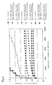
- the results of the measurement of the coefficient of friction of the sample optical disks No. 1 to No. 3 are shown in Fig. 3 (cumulative number of rotation versus coefficient of friction).
- the initial warp was significantly small for each of the sample optical disks No. 1 and No. 2 and remained small after storage in high-temperature, high humidity environment.
- the sample optical disks No. 1 and No. 2 proved to be suitable for practical use. None of the five samples of No. 1 and No. 2 received scratches in the optical head contact test. The samples also showed significantly high initial scratch resistance.
- the coefficient of friction of the sample No. 1 was initially small, indicating that the scratch resistance, or lubricity, of the sample No. 1 was initially as high as that of the sample No. 2.
- the sample No. 1 showed somewhat higher coefficient of friction as compared to the sample No. 2. The difference became significant especially after storage in high-temperature, low humidity environment. The reason for this is considered to be as follows: since the silicone acrylate used in the sample No. 1 was monofunctional, the crosslinking between the silicone acrylate and the base material could not proceed to a sufficient degree.
- All of the five of the sample optical disks No. 3 received scratches in the optical head contact test.
- the hard coat layers of the samples No. 3 used the same base material (a) as that used in the samples No. 1 and No. 2 and thus had a high hardness, the lack of the reactive silicone in the hard coat agent resulted in insufficient lubricity of the hard coat surface, making the samples susceptible to scratches.
- the sample optical disks No. 4 which used the base material (b) with insufficient hardness, received scratches in three samples in the optical head contact test despite the addition of the reactive silicone to impart lubricity to the hard coat surface.
- the hard coat layer was given to the phase-change type optical disks.
- the present invention can be applied to read-only type optical disks or write-once type optical disks as well as optical disks having a phase-change type recording layer. Therefore, the above-mentioned working examples are merely examples in all points, and the present invention should not be restrictedly interpreted by the examples. Furthermore, all modifications belonging to a scope equivalent to that of the claims are within the scope of the present invention.
- an optical information medium that is less susceptible to warp in the disk surface while offering significantly high scratch resistance and abrasion resistance is provided.
- a method for producing an optical information medium that is less susceptible to warp in the disk surface while offering significantly high scratch resistance and abrasion resistance is provided.
Landscapes
- Chemical & Material Sciences (AREA)
- Inorganic Chemistry (AREA)
- Engineering & Computer Science (AREA)
- Manufacturing & Machinery (AREA)
- Optical Record Carriers And Manufacture Thereof (AREA)
- Manufacturing Optical Record Carriers (AREA)
- Holo Graphy (AREA)
- Adornments (AREA)
Applications Claiming Priority (3)
| Application Number | Priority Date | Filing Date | Title |
|---|---|---|---|
| JP2002156518 | 2002-05-29 | ||
| JP2002156518 | 2002-05-29 | ||
| PCT/JP2003/006495 WO2003100777A1 (en) | 2002-05-29 | 2003-05-23 | Optical information medium and production method therefor |
Publications (3)
| Publication Number | Publication Date |
|---|---|
| EP1511025A1 true EP1511025A1 (de) | 2005-03-02 |
| EP1511025A4 EP1511025A4 (de) | 2009-09-30 |
| EP1511025B1 EP1511025B1 (de) | 2012-02-01 |
Family
ID=29561487
Family Applications (1)
| Application Number | Title | Priority Date | Filing Date |
|---|---|---|---|
| EP03730618A Expired - Lifetime EP1511025B1 (de) | 2002-05-29 | 2003-05-23 | Optisches informations medium und herstellungsverfahren dafür |
Country Status (9)
| Country | Link |
|---|---|
| US (1) | US7153558B2 (de) |
| EP (1) | EP1511025B1 (de) |
| JP (1) | JP4204545B2 (de) |
| KR (1) | KR20050009715A (de) |
| CN (1) | CN100437784C (de) |
| AT (1) | ATE544150T1 (de) |
| AU (1) | AU2003241756A1 (de) |
| TW (1) | TWI338892B (de) |
| WO (1) | WO2003100777A1 (de) |
Families Citing this family (8)
| Publication number | Priority date | Publication date | Assignee | Title |
|---|---|---|---|---|
| WO2004047095A1 (ja) * | 2002-11-18 | 2004-06-03 | Asahi Glass Company, Limited | 皮脂汚れ防止性を付与されたハードコート層を有する光ディスク |
| WO2004047094A1 (ja) * | 2002-11-18 | 2004-06-03 | Asahi Glass Company, Limited | 表面潤滑性を付与されたハードコート層を有する光ディスク |
| JP4794116B2 (ja) * | 2003-05-14 | 2011-10-19 | Tdk株式会社 | 光情報媒体 |
| JP2005111756A (ja) * | 2003-10-06 | 2005-04-28 | Fuji Photo Film Co Ltd | ハードコート処理物品、硬化性組成物、および情報記録担体 |
| JP4319522B2 (ja) * | 2003-10-31 | 2009-08-26 | Tdk株式会社 | 光情報媒体 |
| JP4715990B2 (ja) * | 2004-01-09 | 2011-07-06 | 信越化学工業株式会社 | 光記録媒体用硬化性樹脂組成物及び光記録媒体 |
| JP2005255706A (ja) * | 2004-03-09 | 2005-09-22 | Lintec Corp | 粘接着剤組成物、光ディスク製造用シートおよび光ディスク |
| US20070134463A1 (en) * | 2005-12-09 | 2007-06-14 | General Electric Company | Storage media and associated method |
Family Cites Families (29)
| Publication number | Priority date | Publication date | Assignee | Title |
|---|---|---|---|---|
| JP2901417B2 (ja) | 1992-05-19 | 1999-06-07 | ティーディーケイ株式会社 | 光記録ディスクの製造方法 |
| JPH0641467A (ja) * | 1992-07-24 | 1994-02-15 | Shin Etsu Chem Co Ltd | 紫外線硬化性コーティング組成物及び保護皮膜 |
| JPH07169100A (ja) * | 1993-10-18 | 1995-07-04 | Mitsui Toatsu Chem Inc | 光情報記録媒体 |
| JPH07254169A (ja) | 1994-03-15 | 1995-10-03 | Kao Corp | 表面処理基体 |
| JPH08203121A (ja) | 1995-01-30 | 1996-08-09 | Dainippon Printing Co Ltd | 光記録媒体 |
| JPH08235639A (ja) * | 1995-03-02 | 1996-09-13 | Dainippon Printing Co Ltd | 光記録媒体及びその作成方法 |
| JPH08124216A (ja) * | 1994-10-21 | 1996-05-17 | Ricoh Co Ltd | 光情報記録媒体 |
| US5609990A (en) * | 1995-02-08 | 1997-03-11 | Imation Corp. | Optical recording disk having a sealcoat layer |
| JPH0954984A (ja) | 1995-06-07 | 1997-02-25 | Dainippon Printing Co Ltd | 光記録媒体 |
| JP3474330B2 (ja) | 1995-10-03 | 2003-12-08 | Jsr株式会社 | 反応性シリカ粒子、その製法および用途 |
| US6160067A (en) * | 1995-10-03 | 2000-12-12 | Dsm N.V. | Reactive silica particles, process for manufacturing the same, use of the same |
| JPH10110118A (ja) | 1996-08-13 | 1998-04-28 | Toray Ind Inc | 防汚性ハードコート剤および光記録媒体 |
| JPH10326435A (ja) * | 1997-03-25 | 1998-12-08 | Sony Corp | 光学記録媒体及び光学ディスク装置 |
| JPH10287822A (ja) * | 1997-04-15 | 1998-10-27 | Mitsubishi Chem Corp | 活性エネルギー線硬化性被覆組成物 |
| JPH11134714A (ja) * | 1997-10-31 | 1999-05-21 | Taiyo Yuden Co Ltd | 光情報媒体とその製造方法 |
| JPH11213444A (ja) | 1998-01-30 | 1999-08-06 | Sony Corp | 光記録媒体 |
| JP3436492B2 (ja) * | 1998-08-24 | 2003-08-11 | 三菱レイヨン株式会社 | 耐摩耗性薄膜を有する薄型物品、及び光学ディスク |
| US6376060B1 (en) * | 1998-09-25 | 2002-04-23 | Dai Nippon Printing Co., Ltd. | Hardcoat film |
| US6623791B2 (en) * | 1999-07-30 | 2003-09-23 | Ppg Industries Ohio, Inc. | Coating compositions having improved adhesion, coated substrates and methods related thereto |
| MX238958B (es) * | 1999-07-30 | 2006-07-27 | Ppg Ind Ohio Inc | Recubrimientos curados que tienen una mejorada resistencia al rayado, sustratos recubiertos y metodos relacionados con los mismos. |
| JP4590758B2 (ja) * | 2000-04-10 | 2010-12-01 | Tdk株式会社 | 光情報媒体 |
| JP2002260280A (ja) | 2000-06-28 | 2002-09-13 | Tdk Corp | 光情報媒体およびその評価方法 |
| JP2002157782A (ja) | 2000-09-05 | 2002-05-31 | Tdk Corp | 光情報媒体およびその試験方法 |
| JP3897583B2 (ja) | 2000-11-30 | 2007-03-28 | 三菱レイヨン株式会社 | 光ディスク |
| EP1350816B1 (de) * | 2000-11-30 | 2010-06-02 | Mitsubishi Rayon Co., Ltd. | Strahlungshärtbarer lack für optische platten sowie optische platte |
| JP2002230837A (ja) | 2001-01-30 | 2002-08-16 | Asahi Glass Co Ltd | ハードコート層を有する青色レーザーディスク((登録商標)およびその製造方法 |
| JP2003077184A (ja) * | 2001-08-31 | 2003-03-14 | Tdk Corp | 光記録媒体及びその製造方法 |
| US7452609B2 (en) * | 2001-12-26 | 2008-11-18 | Tdk Corporation | Article having composite hard coat layer and method for forming composite hard coat layer |
| JP4475016B2 (ja) * | 2003-06-30 | 2010-06-09 | 東レ株式会社 | ハードコートフィルム、反射防止フィルムおよび画像表示装置 |
-
2003
- 2003-05-23 AU AU2003241756A patent/AU2003241756A1/en not_active Abandoned
- 2003-05-23 KR KR10-2004-7019064A patent/KR20050009715A/ko not_active Ceased
- 2003-05-23 CN CNB038083426A patent/CN100437784C/zh not_active Expired - Fee Related
- 2003-05-23 JP JP2004508342A patent/JP4204545B2/ja not_active Expired - Fee Related
- 2003-05-23 EP EP03730618A patent/EP1511025B1/de not_active Expired - Lifetime
- 2003-05-23 US US10/504,054 patent/US7153558B2/en not_active Expired - Lifetime
- 2003-05-23 AT AT03730618T patent/ATE544150T1/de active
- 2003-05-23 WO PCT/JP2003/006495 patent/WO2003100777A1/ja not_active Ceased
- 2003-05-27 TW TW092114208A patent/TWI338892B/zh not_active IP Right Cessation
Non-Patent Citations (2)
| Title |
|---|
| No further relevant documents disclosed * |
| See also references of WO03100777A1 * |
Also Published As
| Publication number | Publication date |
|---|---|
| KR20050009715A (ko) | 2005-01-25 |
| US20050089665A1 (en) | 2005-04-28 |
| WO2003100777A1 (en) | 2003-12-04 |
| EP1511025B1 (de) | 2012-02-01 |
| ATE544150T1 (de) | 2012-02-15 |
| CN100437784C (zh) | 2008-11-26 |
| JP4204545B2 (ja) | 2009-01-07 |
| TWI338892B (en) | 2011-03-11 |
| JPWO2003100777A1 (ja) | 2005-09-29 |
| AU2003241756A1 (en) | 2003-12-12 |
| CN1647177A (zh) | 2005-07-27 |
| US7153558B2 (en) | 2006-12-26 |
| EP1511025A4 (de) | 2009-09-30 |
| TW200402710A (en) | 2004-02-16 |
Similar Documents
| Publication | Publication Date | Title |
|---|---|---|
| JP4590849B2 (ja) | ハードコート剤組成物及びこれを用いた光情報媒体 | |
| JP4779293B2 (ja) | ハードコート剤組成物及びこれを用いた光情報媒体 | |
| CN1898342B (zh) | 硬膜剂组合物和采用该组合物的光信息介质 | |
| US7026030B2 (en) | Optical information medium | |
| EP1462245B1 (de) | Artikel mit harter verbundbeschichtungsschicht und verfahren zur herstellung der harten verbundbeschichtungsschicht | |
| EP1511025B1 (de) | Optisches informations medium und herstellungsverfahren dafür | |
| EP1571659B1 (de) | Verfahren zur bewertung eines optischen informationsmediums und optisches informationsmedium | |
| WO2003049099A1 (en) | Optical disk having hard coat layer exhibiting effective lubricity | |
| JP4496766B2 (ja) | 保護層の形成方法及び光情報媒体の製造方法 | |
| JP4185496B2 (ja) | 光情報媒体の製造方法 | |
| JP2008287883A (ja) | 光情報媒体 | |
| JP4794116B2 (ja) | 光情報媒体 | |
| WO2004010425A1 (ja) | 光情報媒体用の活性エネルギー線硬化性組成物及びこれを用いた光情報媒体 | |
| JP2004335021A (ja) | 光記録ディスク | |
| JP2005011440A (ja) | 光記録ディスク | |
| JP2005011442A (ja) | 光記録ディスク | |
| JP2005011446A (ja) | 光記録ディスク |
Legal Events
| Date | Code | Title | Description |
|---|---|---|---|
| PUAI | Public reference made under article 153(3) epc to a published international application that has entered the european phase |
Free format text: ORIGINAL CODE: 0009012 |
|
| 17P | Request for examination filed |
Effective date: 20041223 |
|
| AK | Designated contracting states |
Kind code of ref document: A1 Designated state(s): AT BE BG CH CY CZ DE DK EE ES FI FR GB GR HU IE IT LI LU MC NL PT RO SE SI SK TR |
|
| AX | Request for extension of the european patent |
Extension state: AL LT LV MK |
|
| RIN1 | Information on inventor provided before grant (corrected) |
Inventor name: TANAKA, KAZUSHI,C/O TDK CORPORATION Inventor name: IHARA, RIE,C/O TDK CORPORATION Inventor name: HAYASHIDA, NAOKI,C/O TDK CORPORATION |
|
| DAX | Request for extension of the european patent (deleted) | ||
| A4 | Supplementary search report drawn up and despatched |
Effective date: 20090827 |
|
| 17Q | First examination report despatched |
Effective date: 20100504 |
|
| GRAP | Despatch of communication of intention to grant a patent |
Free format text: ORIGINAL CODE: EPIDOSNIGR1 |
|
| RIN1 | Information on inventor provided before grant (corrected) |
Inventor name: IHARA, RIE,C/O TDK CORPORATION Inventor name: HAYASHIDA, NAOKIC/O TDK CORPORATION Inventor name: TANAKA, KAZUSHI,C/O TDK CORPORATION |
|
| GRAS | Grant fee paid |
Free format text: ORIGINAL CODE: EPIDOSNIGR3 |
|
| GRAA | (expected) grant |
Free format text: ORIGINAL CODE: 0009210 |
|
| AK | Designated contracting states |
Kind code of ref document: B1 Designated state(s): AT BE BG CH CY CZ DE DK EE ES FI FR GB GR HU IE IT LI LU MC NL PT RO SE SI SK TR |
|
| REG | Reference to a national code |
Ref country code: GB Ref legal event code: FG4D |
|
| REG | Reference to a national code |
Ref country code: AT Ref legal event code: REF Ref document number: 544150 Country of ref document: AT Kind code of ref document: T Effective date: 20120215 Ref country code: CH Ref legal event code: EP |
|
| REG | Reference to a national code |
Ref country code: DE Ref legal event code: R096 Ref document number: 60339899 Country of ref document: DE Effective date: 20120405 |
|
| REG | Reference to a national code |
Ref country code: NL Ref legal event code: VDEP Effective date: 20120201 |
|
| PG25 | Lapsed in a contracting state [announced via postgrant information from national office to epo] |
Ref country code: NL Free format text: LAPSE BECAUSE OF FAILURE TO SUBMIT A TRANSLATION OF THE DESCRIPTION OR TO PAY THE FEE WITHIN THE PRESCRIBED TIME-LIMIT Effective date: 20120201 |
|
| PG25 | Lapsed in a contracting state [announced via postgrant information from national office to epo] |
Ref country code: BE Free format text: LAPSE BECAUSE OF FAILURE TO SUBMIT A TRANSLATION OF THE DESCRIPTION OR TO PAY THE FEE WITHIN THE PRESCRIBED TIME-LIMIT Effective date: 20120201 Ref country code: PT Free format text: LAPSE BECAUSE OF FAILURE TO SUBMIT A TRANSLATION OF THE DESCRIPTION OR TO PAY THE FEE WITHIN THE PRESCRIBED TIME-LIMIT Effective date: 20120601 Ref country code: GR Free format text: LAPSE BECAUSE OF FAILURE TO SUBMIT A TRANSLATION OF THE DESCRIPTION OR TO PAY THE FEE WITHIN THE PRESCRIBED TIME-LIMIT Effective date: 20120502 Ref country code: FI Free format text: LAPSE BECAUSE OF FAILURE TO SUBMIT A TRANSLATION OF THE DESCRIPTION OR TO PAY THE FEE WITHIN THE PRESCRIBED TIME-LIMIT Effective date: 20120201 |
|
| REG | Reference to a national code |
Ref country code: AT Ref legal event code: MK05 Ref document number: 544150 Country of ref document: AT Kind code of ref document: T Effective date: 20120201 |
|
| PG25 | Lapsed in a contracting state [announced via postgrant information from national office to epo] |
Ref country code: CY Free format text: LAPSE BECAUSE OF FAILURE TO SUBMIT A TRANSLATION OF THE DESCRIPTION OR TO PAY THE FEE WITHIN THE PRESCRIBED TIME-LIMIT Effective date: 20120201 |
|
| PG25 | Lapsed in a contracting state [announced via postgrant information from national office to epo] |
Ref country code: CZ Free format text: LAPSE BECAUSE OF FAILURE TO SUBMIT A TRANSLATION OF THE DESCRIPTION OR TO PAY THE FEE WITHIN THE PRESCRIBED TIME-LIMIT Effective date: 20120201 Ref country code: SI Free format text: LAPSE BECAUSE OF FAILURE TO SUBMIT A TRANSLATION OF THE DESCRIPTION OR TO PAY THE FEE WITHIN THE PRESCRIBED TIME-LIMIT Effective date: 20120201 Ref country code: RO Free format text: LAPSE BECAUSE OF FAILURE TO SUBMIT A TRANSLATION OF THE DESCRIPTION OR TO PAY THE FEE WITHIN THE PRESCRIBED TIME-LIMIT Effective date: 20120201 Ref country code: DK Free format text: LAPSE BECAUSE OF FAILURE TO SUBMIT A TRANSLATION OF THE DESCRIPTION OR TO PAY THE FEE WITHIN THE PRESCRIBED TIME-LIMIT Effective date: 20120201 Ref country code: SE Free format text: LAPSE BECAUSE OF FAILURE TO SUBMIT A TRANSLATION OF THE DESCRIPTION OR TO PAY THE FEE WITHIN THE PRESCRIBED TIME-LIMIT Effective date: 20120201 Ref country code: EE Free format text: LAPSE BECAUSE OF FAILURE TO SUBMIT A TRANSLATION OF THE DESCRIPTION OR TO PAY THE FEE WITHIN THE PRESCRIBED TIME-LIMIT Effective date: 20120201 |
|
| PG25 | Lapsed in a contracting state [announced via postgrant information from national office to epo] |
Ref country code: SK Free format text: LAPSE BECAUSE OF FAILURE TO SUBMIT A TRANSLATION OF THE DESCRIPTION OR TO PAY THE FEE WITHIN THE PRESCRIBED TIME-LIMIT Effective date: 20120201 Ref country code: IT Free format text: LAPSE BECAUSE OF FAILURE TO SUBMIT A TRANSLATION OF THE DESCRIPTION OR TO PAY THE FEE WITHIN THE PRESCRIBED TIME-LIMIT Effective date: 20120201 |
|
| PLBE | No opposition filed within time limit |
Free format text: ORIGINAL CODE: 0009261 |
|
| STAA | Information on the status of an ep patent application or granted ep patent |
Free format text: STATUS: NO OPPOSITION FILED WITHIN TIME LIMIT |
|
| PG25 | Lapsed in a contracting state [announced via postgrant information from national office to epo] |
Ref country code: MC Free format text: LAPSE BECAUSE OF NON-PAYMENT OF DUE FEES Effective date: 20120531 |
|
| REG | Reference to a national code |
Ref country code: CH Ref legal event code: PL |
|
| 26N | No opposition filed |
Effective date: 20121105 |
|
| REG | Reference to a national code |
Ref country code: DE Ref legal event code: R082 Ref document number: 60339899 Country of ref document: DE Representative=s name: KILIAN KILIAN & PARTNER MBB PATENTANWAELTE, DE Ref country code: DE Ref legal event code: R082 Ref document number: 60339899 Country of ref document: DE Representative=s name: KILIAN KILIAN & PARTNER, DE |
|
| PG25 | Lapsed in a contracting state [announced via postgrant information from national office to epo] |
Ref country code: CH Free format text: LAPSE BECAUSE OF NON-PAYMENT OF DUE FEES Effective date: 20120531 Ref country code: LI Free format text: LAPSE BECAUSE OF NON-PAYMENT OF DUE FEES Effective date: 20120531 Ref country code: AT Free format text: LAPSE BECAUSE OF FAILURE TO SUBMIT A TRANSLATION OF THE DESCRIPTION OR TO PAY THE FEE WITHIN THE PRESCRIBED TIME-LIMIT Effective date: 20120201 |
|
| REG | Reference to a national code |
Ref country code: IE Ref legal event code: MM4A |
|
| REG | Reference to a national code |
Ref country code: DE Ref legal event code: R097 Ref document number: 60339899 Country of ref document: DE Effective date: 20121105 |
|
| PG25 | Lapsed in a contracting state [announced via postgrant information from national office to epo] |
Ref country code: IE Free format text: LAPSE BECAUSE OF NON-PAYMENT OF DUE FEES Effective date: 20120523 Ref country code: ES Free format text: LAPSE BECAUSE OF FAILURE TO SUBMIT A TRANSLATION OF THE DESCRIPTION OR TO PAY THE FEE WITHIN THE PRESCRIBED TIME-LIMIT Effective date: 20120512 |
|
| PG25 | Lapsed in a contracting state [announced via postgrant information from national office to epo] |
Ref country code: BG Free format text: LAPSE BECAUSE OF FAILURE TO SUBMIT A TRANSLATION OF THE DESCRIPTION OR TO PAY THE FEE WITHIN THE PRESCRIBED TIME-LIMIT Effective date: 20120501 |
|
| PG25 | Lapsed in a contracting state [announced via postgrant information from national office to epo] |
Ref country code: TR Free format text: LAPSE BECAUSE OF FAILURE TO SUBMIT A TRANSLATION OF THE DESCRIPTION OR TO PAY THE FEE WITHIN THE PRESCRIBED TIME-LIMIT Effective date: 20120201 |
|
| PG25 | Lapsed in a contracting state [announced via postgrant information from national office to epo] |
Ref country code: LU Free format text: LAPSE BECAUSE OF NON-PAYMENT OF DUE FEES Effective date: 20120523 |
|
| PG25 | Lapsed in a contracting state [announced via postgrant information from national office to epo] |
Ref country code: HU Free format text: LAPSE BECAUSE OF FAILURE TO SUBMIT A TRANSLATION OF THE DESCRIPTION OR TO PAY THE FEE WITHIN THE PRESCRIBED TIME-LIMIT Effective date: 20030523 |
|
| REG | Reference to a national code |
Ref country code: FR Ref legal event code: PLFP Year of fee payment: 14 |
|
| REG | Reference to a national code |
Ref country code: FR Ref legal event code: PLFP Year of fee payment: 15 |
|
| REG | Reference to a national code |
Ref country code: FR Ref legal event code: PLFP Year of fee payment: 16 |
|
| PGFP | Annual fee paid to national office [announced via postgrant information from national office to epo] |
Ref country code: DE Payment date: 20190508 Year of fee payment: 17 |
|
| PGFP | Annual fee paid to national office [announced via postgrant information from national office to epo] |
Ref country code: FR Payment date: 20190410 Year of fee payment: 17 |
|
| PGFP | Annual fee paid to national office [announced via postgrant information from national office to epo] |
Ref country code: GB Payment date: 20190522 Year of fee payment: 17 |
|
| REG | Reference to a national code |
Ref country code: DE Ref legal event code: R119 Ref document number: 60339899 Country of ref document: DE |
|
| GBPC | Gb: european patent ceased through non-payment of renewal fee |
Effective date: 20200523 |
|
| PG25 | Lapsed in a contracting state [announced via postgrant information from national office to epo] |
Ref country code: GB Free format text: LAPSE BECAUSE OF NON-PAYMENT OF DUE FEES Effective date: 20200523 Ref country code: FR Free format text: LAPSE BECAUSE OF NON-PAYMENT OF DUE FEES Effective date: 20200531 |
|
| PG25 | Lapsed in a contracting state [announced via postgrant information from national office to epo] |
Ref country code: DE Free format text: LAPSE BECAUSE OF NON-PAYMENT OF DUE FEES Effective date: 20201201 |