EP1501099A1 - Nicht flüchtiges Speichermatrix mit Speicherzellen mit geteiltem Gate sowie Programmierverfahren zur Vermeidung von Störungen - Google Patents
Nicht flüchtiges Speichermatrix mit Speicherzellen mit geteiltem Gate sowie Programmierverfahren zur Vermeidung von Störungen Download PDFInfo
- Publication number
- EP1501099A1 EP1501099A1 EP03016786A EP03016786A EP1501099A1 EP 1501099 A1 EP1501099 A1 EP 1501099A1 EP 03016786 A EP03016786 A EP 03016786A EP 03016786 A EP03016786 A EP 03016786A EP 1501099 A1 EP1501099 A1 EP 1501099A1
- Authority
- EP
- European Patent Office
- Prior art keywords
- voltage
- cell
- cells
- control
- programming
- Prior art date
- Legal status (The legal status is an assumption and is not a legal conclusion. Google has not performed a legal analysis and makes no representation as to the accuracy of the status listed.)
- Granted
Links
- 230000015654 memory Effects 0.000 title claims abstract description 45
- 238000000034 method Methods 0.000 title claims abstract description 8
- 230000000903 blocking effect Effects 0.000 claims abstract description 30
- 230000004913 activation Effects 0.000 claims description 3
- 230000003213 activating effect Effects 0.000 claims 1
- 230000003071 parasitic effect Effects 0.000 description 10
- 230000010354 integration Effects 0.000 description 4
- 230000000694 effects Effects 0.000 description 2
- 230000006978 adaptation Effects 0.000 description 1
- 230000002301 combined effect Effects 0.000 description 1
- 230000001419 dependent effect Effects 0.000 description 1
- 230000006870 function Effects 0.000 description 1
- 239000002784 hot electron Substances 0.000 description 1
- 238000010295 mobile communication Methods 0.000 description 1
- 238000012986 modification Methods 0.000 description 1
- 230000004048 modification Effects 0.000 description 1
- 230000009467 reduction Effects 0.000 description 1
Images


Classifications
-
- G—PHYSICS
- G11—INFORMATION STORAGE
- G11C—STATIC STORES
- G11C16/00—Erasable programmable read-only memories
- G11C16/02—Erasable programmable read-only memories electrically programmable
- G11C16/04—Erasable programmable read-only memories electrically programmable using variable threshold transistors, e.g. FAMOS
- G11C16/0408—Erasable programmable read-only memories electrically programmable using variable threshold transistors, e.g. FAMOS comprising cells containing floating gate transistors
- G11C16/0425—Erasable programmable read-only memories electrically programmable using variable threshold transistors, e.g. FAMOS comprising cells containing floating gate transistors comprising cells containing a merged floating gate and select transistor
-
- G—PHYSICS
- G11—INFORMATION STORAGE
- G11C—STATIC STORES
- G11C16/00—Erasable programmable read-only memories
- G11C16/02—Erasable programmable read-only memories electrically programmable
- G11C16/06—Auxiliary circuits, e.g. for writing into memory
- G11C16/10—Programming or data input circuits
-
- G—PHYSICS
- G11—INFORMATION STORAGE
- G11C—STATIC STORES
- G11C16/00—Erasable programmable read-only memories
- G11C16/02—Erasable programmable read-only memories electrically programmable
- G11C16/06—Auxiliary circuits, e.g. for writing into memory
- G11C16/34—Determination of programming status, e.g. threshold voltage, overprogramming or underprogramming, retention
- G11C16/3418—Disturbance prevention or evaluation; Refreshing of disturbed memory data
Definitions
- the present invention relates, in general, to an integrated circuit comprising an array of non-volatile memory cells with a divided gate, of the type FLASH EEPROM, having a page architecture for erase operations and programming the cells. More particularly, the present invention regards the use of such architectures of memory boards for applications embedded in smart cards to replace traditional birds.
- the present invention also relates to a programming method of a memory cell of such a table.
- Tables of non-volatile memory cells with a divided gate, arranged in one or more rows and columns and electrically connected to each other by group so as to form one or more pages, are already known.
- the US 6,400,603, hereby incorporated by reference, for example describes a table that meets the general definition given above.
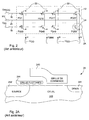
- Figure 1 represents a table architecture 10 organized in 8 columns of 256 pages 12. At these 8 columns correspond 8 columns of control circuits 14 of 128 circuits of control with a control circuit for two pages.
- the different signals of command which will not be detailed here, allow operations to be carried out such as erasing a page or programming a cell page.
- row control lines will be noted 16 and 16b, each being connected to all the control circuits 14 of the row corresponding.
- These rows of command lines 16 and 16b have the function activate or deactivate a row of control circuit 14. Note again the presence of word command lines 18, source command lines 20 and bit control lines 22 to control each column of pages 12 and control circuits 14.
- FIG. 2 represents the detail of a page 12 of a table according to FIG. In the example shown, each page 12 is formed by two rows of cells 24 superimposed.
- FIG. 2A An enlargement of a used memory cell 24 is detailed in FIG. 2A.
- Each of these cells has a first region 241, also called a drain, a second region 242, also called source, spaced from the first region 241, a channel region 243 between the first 241 and second 242 regions, a grid floating 244 and a control gate 245.
- These cells 24 contain binary information that can be modified either programmatically, or by erasing the cell.
- the binary information it contains can take a first determined value, for example 0, by trapping hot electrons in the grid floating 244 of the transistor.
- the binary information can take a second determined value, for example 1, by tunnel effect of Fowler-Nordheim which allows the passage, without ionization, of an electron trapped from the floating gate 244.
- each cell receives first, second and third control signals respectively applied to the control gate 245, on the second region 242, i.e. the source, and on the first region 241, i.e. the drain, of the cell 24 to be programmed.
- page 12 is formed by a group of cells 24 electrically connected to each other.
- This connection between the cells of the same page may be carried out in particular means of a source control line 20 connecting all the sources 242 of the cells of a page between them. It's through this command line of source 20 that the second control signals are applied to the sources 242 cells of the same page.
- the first control signals that are applied to the grid of 245 command of at least one or more cells of the same page, are provided through command lines of words 18. These command lines of words connect each other preferably all the cells 24 forming one and the same row (shown horizontally) inside a page 12.
- the third control signals are applied to the drain 241 of the memory cells of the same column via command lines of bits 22. These bit control lines preferably connect all the cells memories of the pages forming the same column.
- V PROG represents the programming voltage applied to the control gate 245 of the FG16 cell to be programmed via the corresponding word command line 18. Consequently, all the cells 24 of the page sharing the same word command line 18, or the cells FG1 to FG32, receive on their control gate 245 the same control signal V PROG .
- V SS represents a reference voltage, for example the mass, applied to the control gate 245 of all the cells 24 of the page sharing the same word command line 18 as that of the cell to be programmed, ie the cells FG33 at FG64.
- I SINK represents a bias current drawn from the drain 241 of the FG16 cell to be programmed via the bit control line 22 corresponding to this cell. Consequently, all the cells 24 forming a column with the cell to be programmed and sharing the same bit control line 22, here the cell FG48, are applied the same control signal on their drain.
- V DD represents the supply voltage of the memory applied to the drain 241 of all cells not sharing the same bit control line 22, which normally prevents their programming.
- HV represents a high voltage, for example 12 volts, obtained by means of a charge pump comprising the number of suitable amplifier stages. This high voltage is applied to the source 242 of the FG16 cell to be programmed through the source command line 20 of the page containing this cell. Knowing that this source command line connects them all the sources 242 of the cells 24 of the same page, the high voltage HV is therefore also applied on the source of each cell of the page.
- the type of memory presented above is mainly intended for low-power applications, for example in a smart card or for a cellphone.
- G.S.M applications Global System for Mobile Communications
- a general object of the present invention is therefore to propose a solution to ensure good reliability of the information contained in the memory while ensuring a reasonable service life of this memory.
- the aim is in particular to ensure for a low voltage power supply, effective programming of a specific cell without presenting significant risks of parasitic programming of cells with connections common electric with the cell to program and in particular sharing the same command line of words.
- the present invention thus relates to an integrated circuit comprising a array of non-volatile memory cells with a divided gate of the aforementioned type the features are set forth in claim 1.
- the present invention also relates to a programming method memory cells of such an array.
- the invention also relates to an integrated circuit comprising means voltage amplifiers connected to the blocking logic to deliver the first blocking voltage strictly higher than the low supply voltage.
- These voltage amplifier means may be, for example, either a voltage doubler built into the switchboard, a source of high voltage external to the table, of the charge pump type, or advantageously at least one stage of the charge pump used to deliver high voltage to the cell sources.
- FIG. 3A shows, according to a first programming mode, an enlargement of a part of the memory array shown in FIG. 1 and more particularly of a page 12 represented in FIG. 2.
- four memory cells 24 divided grid of the same page are represented.
- These cells 24A, 24B, 24C and 24D are similar to that shown in FIG. 2A. They each have a first region corresponding to their drain D, a second region corresponding to their source S and a third region corresponding to their control gate G.
- the control gates G receive first control signals (V PROG or V SS ) via the word control lines 18.
- the sources S receive second control signals (HV) via a source control line 20.
- the drains D receive third control signals (I SINK or V BLOC1 ) via lines bit control 22.
- the four cells 24A to 24D are connected between them as follows.
- the four cells belong to the same page and so share the same command line of sources 20. Nevertheless, it's all actually envisioned that these cells do not physically share the same line of source control, but that each of the cells forming a page receive, independently of other cells forming this page, a high voltage like second command signal via source command lines distinct.
- the cells 24A and 24B, respectively 24C and 24D, located on the same row share a same word command line 18.
- the cells 24A and 24C, respectively 24B and 24D, located on the same column share the same line bit control 22.
- a so-called programming voltage V PROG slightly lower or substantially equal to the low supply voltage V DD , is applied to the control gate of the cell 24A via the command line of words. corresponding to this cell. It is also applied a HV high voltage on the source of this cell 24A via the source control line 20 and a bias current I SINK is pulled on the drain D of this cell 24A via the bit control line 22 corresponding to this cell.
- the cell 24B receives the programming voltage V PROG on its control gate because it shares the same word command line 18 as the cell 24A to be programmed and the high voltage HV on its source, because it shares the same command line. sources 20 as the cell 24A.
- the third control signal applied via the bit control line 22 is free because the cell 24B does not share the same bit control line 22 as the cell 24A to be programmed.
- a blocking voltage V BLOC1 strictly greater than the low supply voltage V DD of the memory is applied to the drain of this cell 24B via the bit control line 22 corresponding to this cell 24B.
- this first blocking voltage V BLOC1 is at least twice higher than the low supply voltage V DD .
- the cells 24C and 24D have their respective control gates connected to the same word control line 18 different from that connected to the control gate of the cell 24A to be programmed.
- a reference voltage V SS such as the mass
- FIG. 3B also shows, by way of example, the same magnification as that of FIG. 3A according to a second programming mode.
- the numerical references are the same as those used in Figure 3A.
- this other solution consists, in the example shown, in lowering the programming voltage V PROG of the cell 24A to be programmed, this programming voltage V PROG then being significantly lower than the low supply voltage V DD of the memory. It should nevertheless be noted that this programming voltage must remain sufficiently high so as to make the channel of the cell to be programmed conductive.
- the bias current I SINK pulled from the drain of the cell 24A to be programmed via the bit control line 22 causes a reduced voltage on the drain 241 of the cell 24C, which increases the potential difference between the source 242 and the drain 241 of this cell 24C, thus increasing its leakage current I F.
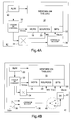
- FIG. 4A shows the integration of a memory array as defined previously in an integrated circuit, according to a first embodiment of the invention.
- the integrated circuit IC is powered by an external or internal low voltage power source V DD .
- the circuit notably comprises the memory array 10 as defined previously, that is to say the memory cells arranged in rows and columns to which must be added the control logic 32 of the cells delivering the various control signals via first, second and third control lines, respectively of words 18, of sources 20 and of bits 22 as well as voltage amplifying means, such as for example a charge pump 34 making it possible to deliver a high voltage HV supplied to the sources of the memory cells comprising a cell to be programmed via the source control line 20.
- the circuit further comprises a blocking logic 36 for delivering a blocking signal V BLOC1 applicable to the drains of cells sharing the same word control line 18. a cell to be programmed via the bit control line 22 according to the first programming variant mentioned above.
- This blocking logic 36 is connected to external voltage amplifying means or internal to the memory.
- it is intended to use the HV high voltage supplied by the charge pump 34, either by deriving the output voltage of a stage of the charge pump, or by providing a voltage divider bridge, not shown, between the output of the charge pump 34 and the bit control lines 22 for receiving the blocking signal V BLOC1 .
- FIG. 4B represents the integration of a table 10 as defined previously in an integrated circuit IC according to a second embodiment of the invention.
- the elements common with FIG. 4A keep the same numerical references.
- it is advantageously provided to feed the integrated circuit IC with any supply voltage V DD , preferably standard, providing at least a predetermined low supply voltage V REF , hereinafter called " reference voltage ".
- a charge pump 34 can be used to generate the HV high voltage supplied to the sources of the cells of the same page which it is intended to program at least one cell.
- this second mode applied to the first programming variant it is additionally provided for comparing means 38 of the supply voltage V DD supplied with the minimum supply voltage or reference voltage V REF for operating the integrated circuit IC . If the supply voltage V DD is strictly greater than the reference voltage V REF , activation means, such as a switch 40, are positioned so as to directly supply the supply voltage V DD to the drains of the cells not to be programmed and sharing the same command line of words 18 as a cell to be programmed, via the bit control lines 22 corresponding to these cells.
- the activation means 40 are positioned in such a way that the supply voltage V DD is amplified through voltage amplifying means, such as for example, a voltage doubler 42 outputting a blocking voltage V BLOC1 strictly greater than the supply voltage V DD , applicable to the cell drains not to be programmed and sharing the same command line of words 18 that a cell to be programmed, via the bit control lines 22 corresponding to these cells.
- voltage amplifying means such as for example, a voltage doubler 42 outputting a blocking voltage V BLOC1 strictly greater than the supply voltage V DD , applicable to the cell drains not to be programmed and sharing the same command line of words 18 that a cell to be programmed, via the bit control lines 22 corresponding to these cells.
- the adaptation of the second embodiment to the second programming variant can be done simply by replacing the voltage doubler 42 by means for generating a negative blocking voltage -V BLOC2 , as for example voltage inverter means, not shown.
- the voltage amplifier means used to obtain the first and second blocking voltages V BLOC1 and -V BLOC2 can be supplied to the blocking means from a unit external to the integrated circuit containing the array of memory cells.
- the high voltage HV applied to the sources of the memory cells via the source control line may be provided by a unit external to the integrated circuit.
Landscapes
- Engineering & Computer Science (AREA)
- Microelectronics & Electronic Packaging (AREA)
- Read Only Memory (AREA)
Priority Applications (3)
| Application Number | Priority Date | Filing Date | Title |
|---|---|---|---|
| EP03016786A EP1501099B1 (de) | 2003-07-23 | 2003-07-23 | Nicht flüchtiges Speichermatrix mit Speicherzellen mit geteiltem Gate sowie Programmierverfahren zur Vermeidung von Störungen |
| DE60318837T DE60318837T2 (de) | 2003-07-23 | 2003-07-23 | Nicht flüchtiges Speichermatrix mit Speicherzellen mit geteiltem Gate sowie Programmierverfahren zur Vermeidung von Störungen |
| US10/896,911 US20050018504A1 (en) | 2003-07-23 | 2004-07-23 | Array of non volatile split-gate memory cells for avoiding parasitic programming and programming method thereof |
Applications Claiming Priority (1)
| Application Number | Priority Date | Filing Date | Title |
|---|---|---|---|
| EP03016786A EP1501099B1 (de) | 2003-07-23 | 2003-07-23 | Nicht flüchtiges Speichermatrix mit Speicherzellen mit geteiltem Gate sowie Programmierverfahren zur Vermeidung von Störungen |
Publications (2)
| Publication Number | Publication Date |
|---|---|
| EP1501099A1 true EP1501099A1 (de) | 2005-01-26 |
| EP1501099B1 EP1501099B1 (de) | 2008-01-23 |
Family
ID=33483932
Family Applications (1)
| Application Number | Title | Priority Date | Filing Date |
|---|---|---|---|
| EP03016786A Expired - Lifetime EP1501099B1 (de) | 2003-07-23 | 2003-07-23 | Nicht flüchtiges Speichermatrix mit Speicherzellen mit geteiltem Gate sowie Programmierverfahren zur Vermeidung von Störungen |
Country Status (3)
| Country | Link |
|---|---|
| US (1) | US20050018504A1 (de) |
| EP (1) | EP1501099B1 (de) |
| DE (1) | DE60318837T2 (de) |
Families Citing this family (24)
| Publication number | Priority date | Publication date | Assignee | Title |
|---|---|---|---|---|
| US20060238702A1 (en) * | 1999-04-30 | 2006-10-26 | Advanced Medical Optics, Inc. | Ophthalmic lens combinations |
| US20030060881A1 (en) * | 1999-04-30 | 2003-03-27 | Advanced Medical Optics, Inc. | Intraocular lens combinations |
| US7763069B2 (en) | 2002-01-14 | 2010-07-27 | Abbott Medical Optics Inc. | Accommodating intraocular lens with outer support structure |
| US7150759B2 (en) * | 2002-01-14 | 2006-12-19 | Advanced Medical Optics, Inc. | Multi-mechanistic accommodating intraocular lenses |
| US20040082993A1 (en) * | 2002-10-25 | 2004-04-29 | Randall Woods | Capsular intraocular lens implant having a refractive liquid therein |
| US20040082995A1 (en) * | 2002-10-25 | 2004-04-29 | Randall Woods | Telescopic intraocular lens implant for treating age-related macular degeneration |
| US7662180B2 (en) * | 2002-12-05 | 2010-02-16 | Abbott Medical Optics Inc. | Accommodating intraocular lens and method of manufacture thereof |
| US20050131535A1 (en) * | 2003-12-15 | 2005-06-16 | Randall Woods | Intraocular lens implant having posterior bendable optic |
| US20070032866A1 (en) * | 2005-08-05 | 2007-02-08 | Valdemar Portney | Accommodating diffractive intraocular lens |
| US9636213B2 (en) * | 2005-09-30 | 2017-05-02 | Abbott Medical Optics Inc. | Deformable intraocular lenses and lens systems |
| US8241355B2 (en) | 2005-10-28 | 2012-08-14 | Abbott Medical Optics Inc. | Haptic for accommodating intraocular lens |
| US20070168027A1 (en) * | 2006-01-13 | 2007-07-19 | Brady Daniel G | Accommodating diffractive intraocular lens |
| CA2674018C (en) * | 2006-12-29 | 2015-05-26 | Advanced Medical Optics, Inc. | Multifocal accommodating intraocular lens |
| US20080161914A1 (en) * | 2006-12-29 | 2008-07-03 | Advanced Medical Optics, Inc. | Pre-stressed haptic for accommodating intraocular lens |
| US7713299B2 (en) * | 2006-12-29 | 2010-05-11 | Abbott Medical Optics Inc. | Haptic for accommodating intraocular lens |
| US8320191B2 (en) | 2007-08-30 | 2012-11-27 | Infineon Technologies Ag | Memory cell arrangement, method for controlling a memory cell, memory array and electronic device |
| US8034108B2 (en) | 2008-03-28 | 2011-10-11 | Abbott Medical Optics Inc. | Intraocular lens having a haptic that includes a cap |
| US8043372B2 (en) | 2008-10-14 | 2011-10-25 | Abbott Medical Optics Inc. | Intraocular lens and capsular ring |
| CA2766654C (en) * | 2009-06-26 | 2017-10-10 | Abbott Medical Optics Inc. | Accommodating intraocular lenses |
| EP2461768B1 (de) | 2009-08-03 | 2020-02-19 | Johnson & Johnson Surgical Vision, Inc. | Intraokularlinse für akkommodatives sehvermögen |
| CA2772315C (en) * | 2009-08-27 | 2017-09-05 | Abbott Medical Optics Inc. | An accommodating intraocular lens with a surface adherent |
| US9084674B2 (en) | 2012-05-02 | 2015-07-21 | Abbott Medical Optics Inc. | Intraocular lens with shape changing capability to provide enhanced accomodation and visual acuity |
| US8945215B2 (en) | 2012-05-10 | 2015-02-03 | Abbott Medical Optics Inc. | Accommodating intraocular lens with a compressible inner structure |
| WO2019048708A1 (en) | 2017-09-11 | 2019-03-14 | Amo Groningen B.V. | METHODS AND APPARATUSES FOR INCREASING POSITION STABILITY OF INTRAOCULAR LENSES |
Citations (4)
| Publication number | Priority date | Publication date | Assignee | Title |
|---|---|---|---|---|
| US6211547B1 (en) * | 1997-11-24 | 2001-04-03 | Winbond Electronics Corporation | Semiconductor memory array with buried drain lines and processing methods therefor |
| US6285593B1 (en) * | 1998-12-31 | 2001-09-04 | Sandisk Corporation | Word-line decoder for multi-bit-per-cell and analog/multi-level memories with improved resolution and signal-to-noise ratio |
| US6400603B1 (en) * | 2000-05-03 | 2002-06-04 | Advanced Technology Materials, Inc. | Electronically-eraseable programmable read-only memory having reduced-page-size program and erase |
| US20020167844A1 (en) * | 2001-05-14 | 2002-11-14 | Han Kyung Joon | Method and apparatus for multiple byte or page mode programming and reading and for erasing of a flash memory array |
Family Cites Families (2)
| Publication number | Priority date | Publication date | Assignee | Title |
|---|---|---|---|---|
| US7071060B1 (en) * | 1996-02-28 | 2006-07-04 | Sandisk Corporation | EEPROM with split gate source side infection with sidewall spacers |
| US5596532A (en) * | 1995-10-18 | 1997-01-21 | Sandisk Corporation | Flash EEPROM self-adaptive voltage generation circuit operative within a continuous voltage source range |
-
2003
- 2003-07-23 EP EP03016786A patent/EP1501099B1/de not_active Expired - Lifetime
- 2003-07-23 DE DE60318837T patent/DE60318837T2/de not_active Expired - Lifetime
-
2004
- 2004-07-23 US US10/896,911 patent/US20050018504A1/en not_active Abandoned
Patent Citations (4)
| Publication number | Priority date | Publication date | Assignee | Title |
|---|---|---|---|---|
| US6211547B1 (en) * | 1997-11-24 | 2001-04-03 | Winbond Electronics Corporation | Semiconductor memory array with buried drain lines and processing methods therefor |
| US6285593B1 (en) * | 1998-12-31 | 2001-09-04 | Sandisk Corporation | Word-line decoder for multi-bit-per-cell and analog/multi-level memories with improved resolution and signal-to-noise ratio |
| US6400603B1 (en) * | 2000-05-03 | 2002-06-04 | Advanced Technology Materials, Inc. | Electronically-eraseable programmable read-only memory having reduced-page-size program and erase |
| US20020167844A1 (en) * | 2001-05-14 | 2002-11-14 | Han Kyung Joon | Method and apparatus for multiple byte or page mode programming and reading and for erasing of a flash memory array |
Also Published As
| Publication number | Publication date |
|---|---|
| DE60318837D1 (de) | 2008-03-13 |
| DE60318837T2 (de) | 2009-01-22 |
| EP1501099B1 (de) | 2008-01-23 |
| US20050018504A1 (en) | 2005-01-27 |
Similar Documents
| Publication | Publication Date | Title |
|---|---|---|
| EP1501099B1 (de) | Nicht flüchtiges Speichermatrix mit Speicherzellen mit geteiltem Gate sowie Programmierverfahren zur Vermeidung von Störungen | |
| FR2480504A1 (fr) | Transistor programmable et effacable electriquement | |
| EP0272955B1 (de) | Spannungsschalter in MOS-Technologie | |
| JPH0513776A (ja) | 半導体記憶装置 | |
| FR3029343A1 (fr) | Dispositif compact de memoire de type electriquement effacable et programmable | |
| FR2652189A1 (fr) | Memoire eeprom "flash" a effacement par blocs. | |
| EP2337032A1 (de) | Verfahren zur Programmierung einer nichtflüchtigen elektrisch löschbaren und programmierbaren Speicherzelle und und dementsprechende Speicheranordnung | |
| FR3071355B1 (fr) | Cellule-memoire eeprom compacte | |
| FR2987696A1 (fr) | Procede de lecture ecriture de cellules memoire non volatiles | |
| FR3049380A1 (fr) | Amelioration des performances en lecture d'un dispositif de memoire non volatile, en particulier un dispositif de memoire non volatile avec transistor de selection enterre | |
| EP0251853A1 (de) | Integrierte Schaltung zur Speicherung und zur vertraulichen Verarbeitung von Informationen, die eine Antibetrugsvorrichtung enthält | |
| FR2843648A1 (fr) | Dispositif a memoire flash ayant une ligne de source stable independamment du couplage de la ligne de bits et d'un effet de charge | |
| FR2987700A1 (fr) | Memoire non volatile comprenant des mini caissons a potentiel flottant | |
| JP3162264B2 (ja) | フラッシュメモリの書換え方法 | |
| US7274603B2 (en) | Level shifter circuit and semiconductor memory device using same | |
| FR3095526A1 (fr) | Procédé d’écriture dans une mémoire EEPROM et circuit intégré correspondant | |
| FR3048115A1 (fr) | Dispositif et procede de gestion du claquage de transistors d'acces de memoire eeprom. | |
| FR3070537A1 (fr) | Memoire non-volatile a encombrement restreint | |
| EP0265312A1 (de) | Integrierte Schaltung vom Logik-Typ mit EEPROM | |
| EP1727152B1 (de) | EEPROM-Speicherarchitektur | |
| EP0750313B1 (de) | EEPROM-Speicher, der mit Fowler-Nordheim Effekt programmiert und gelöscht wird | |
| WO2004021361A2 (fr) | Memoire eeprom comprenant un registre non volatile integre dans son plan memoire | |
| US20090052259A1 (en) | Non-volatile semiconductor memory device | |
| EP0543703A1 (de) | Elektrisch programmierbarer integrierter Eintransistorspeicher | |
| JP5477483B2 (ja) | 不揮発性半導体メモリ素子、および不揮発性半導体メモリ装置 |
Legal Events
| Date | Code | Title | Description |
|---|---|---|---|
| PUAI | Public reference made under article 153(3) epc to a published international application that has entered the european phase |
Free format text: ORIGINAL CODE: 0009012 |
|
| AK | Designated contracting states |
Kind code of ref document: A1 Designated state(s): AT BE BG CH CY CZ DE DK EE ES FI FR GB GR HU IE IT LI LU MC NL PT RO SE SI SK TR |
|
| AX | Request for extension of the european patent |
Extension state: AL LT LV MK |
|
| RBV | Designated contracting states (corrected) |
Designated state(s): AT BE BG CH CY CZ DE DK EE ES FI FR GB GR HU IE IT LI LU MC NL PT RO SE SI SK TR |
|
| 17P | Request for examination filed |
Effective date: 20050726 |
|
| AKX | Designation fees paid |
Designated state(s): CH DE FR GB IT LI |
|
| 17Q | First examination report despatched |
Effective date: 20061124 |
|
| GRAP | Despatch of communication of intention to grant a patent |
Free format text: ORIGINAL CODE: EPIDOSNIGR1 |
|
| GRAC | Information related to communication of intention to grant a patent modified |
Free format text: ORIGINAL CODE: EPIDOSCIGR1 |
|
| GRAS | Grant fee paid |
Free format text: ORIGINAL CODE: EPIDOSNIGR3 |
|
| GRAA | (expected) grant |
Free format text: ORIGINAL CODE: 0009210 |
|
| AK | Designated contracting states |
Kind code of ref document: B1 Designated state(s): CH DE FR GB IT LI |
|
| REG | Reference to a national code |
Ref country code: GB Ref legal event code: FG4D Free format text: NOT ENGLISH |
|
| REG | Reference to a national code |
Ref country code: CH Ref legal event code: EP |
|
| REF | Corresponds to: |
Ref document number: 60318837 Country of ref document: DE Date of ref document: 20080313 Kind code of ref document: P |
|
| GBT | Gb: translation of ep patent filed (gb section 77(6)(a)/1977) |
Effective date: 20080420 |
|
| REG | Reference to a national code |
Ref country code: CH Ref legal event code: NV Representative=s name: ICB INGENIEURS CONSEILS EN BREVETS SA |
|
| PLBE | No opposition filed within time limit |
Free format text: ORIGINAL CODE: 0009261 |
|
| STAA | Information on the status of an ep patent application or granted ep patent |
Free format text: STATUS: NO OPPOSITION FILED WITHIN TIME LIMIT |
|
| 26N | No opposition filed |
Effective date: 20081024 |
|
| PG25 | Lapsed in a contracting state [announced via postgrant information from national office to epo] |
Ref country code: IT Free format text: LAPSE BECAUSE OF FAILURE TO SUBMIT A TRANSLATION OF THE DESCRIPTION OR TO PAY THE FEE WITHIN THE PRESCRIBED TIME-LIMIT Effective date: 20080123 |
|
| PGFP | Annual fee paid to national office [announced via postgrant information from national office to epo] |
Ref country code: GB Payment date: 20110701 Year of fee payment: 9 |
|
| GBPC | Gb: european patent ceased through non-payment of renewal fee |
Effective date: 20120723 |
|
| PG25 | Lapsed in a contracting state [announced via postgrant information from national office to epo] |
Ref country code: GB Free format text: LAPSE BECAUSE OF NON-PAYMENT OF DUE FEES Effective date: 20120723 |
|
| REG | Reference to a national code |
Ref country code: FR Ref legal event code: PLFP Year of fee payment: 13 |
|
| REG | Reference to a national code |
Ref country code: FR Ref legal event code: PLFP Year of fee payment: 14 |
|
| REG | Reference to a national code |
Ref country code: FR Ref legal event code: PLFP Year of fee payment: 15 |
|
| REG | Reference to a national code |
Ref country code: FR Ref legal event code: PLFP Year of fee payment: 16 |
|
| PGFP | Annual fee paid to national office [announced via postgrant information from national office to epo] |
Ref country code: FR Payment date: 20220622 Year of fee payment: 20 |
|
| PGFP | Annual fee paid to national office [announced via postgrant information from national office to epo] |
Ref country code: DE Payment date: 20220621 Year of fee payment: 20 |
|
| PGFP | Annual fee paid to national office [announced via postgrant information from national office to epo] |
Ref country code: CH Payment date: 20220802 Year of fee payment: 20 |
|
| P01 | Opt-out of the competence of the unified patent court (upc) registered |
Effective date: 20230611 |
|
| REG | Reference to a national code |
Ref country code: DE Ref legal event code: R071 Ref document number: 60318837 Country of ref document: DE |
|
| REG | Reference to a national code |
Ref country code: CH Ref legal event code: PL |