EP1500971A1 - Partikel zur bildanzeige und vorrichtung dafür - Google Patents
Partikel zur bildanzeige und vorrichtung dafür Download PDFInfo
- Publication number
- EP1500971A1 EP1500971A1 EP03719124A EP03719124A EP1500971A1 EP 1500971 A1 EP1500971 A1 EP 1500971A1 EP 03719124 A EP03719124 A EP 03719124A EP 03719124 A EP03719124 A EP 03719124A EP 1500971 A1 EP1500971 A1 EP 1500971A1
- Authority
- EP
- European Patent Office
- Prior art keywords
- particles
- particle
- image
- substrate
- image display
- Prior art date
- Legal status (The legal status is an assumption and is not a legal conclusion. Google has not performed a legal analysis and makes no representation as to the accuracy of the status listed.)
- Granted
Links
Images


Classifications
-
- G—PHYSICS
- G02—OPTICS
- G02F—OPTICAL DEVICES OR ARRANGEMENTS FOR THE CONTROL OF LIGHT BY MODIFICATION OF THE OPTICAL PROPERTIES OF THE MEDIA OF THE ELEMENTS INVOLVED THEREIN; NON-LINEAR OPTICS; FREQUENCY-CHANGING OF LIGHT; OPTICAL LOGIC ELEMENTS; OPTICAL ANALOGUE/DIGITAL CONVERTERS
- G02F1/00—Devices or arrangements for the control of the intensity, colour, phase, polarisation or direction of light arriving from an independent light source, e.g. switching, gating or modulating; Non-linear optics
- G02F1/01—Devices or arrangements for the control of the intensity, colour, phase, polarisation or direction of light arriving from an independent light source, e.g. switching, gating or modulating; Non-linear optics for the control of the intensity, phase, polarisation or colour
- G02F1/165—Devices or arrangements for the control of the intensity, colour, phase, polarisation or direction of light arriving from an independent light source, e.g. switching, gating or modulating; Non-linear optics for the control of the intensity, phase, polarisation or colour based on translational movement of particles in a fluid under the influence of an applied field
- G02F1/1685—Operation of cells; Circuit arrangements affecting the entire cell
-
- G—PHYSICS
- G02—OPTICS
- G02F—OPTICAL DEVICES OR ARRANGEMENTS FOR THE CONTROL OF LIGHT BY MODIFICATION OF THE OPTICAL PROPERTIES OF THE MEDIA OF THE ELEMENTS INVOLVED THEREIN; NON-LINEAR OPTICS; FREQUENCY-CHANGING OF LIGHT; OPTICAL LOGIC ELEMENTS; OPTICAL ANALOGUE/DIGITAL CONVERTERS
- G02F1/00—Devices or arrangements for the control of the intensity, colour, phase, polarisation or direction of light arriving from an independent light source, e.g. switching, gating or modulating; Non-linear optics
- G02F1/01—Devices or arrangements for the control of the intensity, colour, phase, polarisation or direction of light arriving from an independent light source, e.g. switching, gating or modulating; Non-linear optics for the control of the intensity, phase, polarisation or colour
- G02F1/165—Devices or arrangements for the control of the intensity, colour, phase, polarisation or direction of light arriving from an independent light source, e.g. switching, gating or modulating; Non-linear optics for the control of the intensity, phase, polarisation or colour based on translational movement of particles in a fluid under the influence of an applied field
- G02F1/166—Devices or arrangements for the control of the intensity, colour, phase, polarisation or direction of light arriving from an independent light source, e.g. switching, gating or modulating; Non-linear optics for the control of the intensity, phase, polarisation or colour based on translational movement of particles in a fluid under the influence of an applied field characterised by the electro-optical or magneto-optical effect
- G02F1/1671—Devices or arrangements for the control of the intensity, colour, phase, polarisation or direction of light arriving from an independent light source, e.g. switching, gating or modulating; Non-linear optics for the control of the intensity, phase, polarisation or colour based on translational movement of particles in a fluid under the influence of an applied field characterised by the electro-optical or magneto-optical effect involving dry toners
Definitions
- the present invention relates to an image display device which comprises an image display panel enables to repeatedly display or delete images accompanied by flight and movement of particles utilizing Coulomb's force and so on.
- image display devices substitutable for liquid crystal display (LCD)
- image display devices with the use of technology such as an electrophoresis method, an electro-chromic method, a thermal method, dichroic-particles-rotary method are proposed.
- electrophoresis method is proposed that micro-encapsulate dispersion liquid made up with dispersion particles and coloration solution and dispose the liquid between faced substrates.
- a response speed is slow by the reason of viscosity resistance because the particles migrate among the electrophoresis solution.
- there is a problem of lacking imaging repetition stability because particles with high specific gravity of titanium oxide is scattered within solution of low specific gravity, it is easy to subside, difficult to maintain a stability of dispersion state.
- cell size is diminished to a microcapsule level in order to make it hard to appear, however, an essential problem was not overcome at all.
- the dry-type display device mentioned above has an operation mechanism such that a mixture of two kinds of the particles having different colors and different charge characteristics is sandwiched by electrode plates and an electric field is generated between the electrode plates by applying a voltage to the electrode plates, thereby flying the charged particles having different charge characteristics in a different direction to obtain a display element.
- the drive voltage is lowered.
- the drive voltage As a large factor for defining the drive voltage, there are mainly an intermolecular force and a liquid bridging force. If these factors are made to be lowered, a decrease of the drive voltage is instantly achieved. Therefore, it is very important to improve these characteristics.
- an electrostatic property is made to be higher to some extent. Therefore, it is another task to obtain the particles having an excellent electrostatic property.
- the electrostatic property of the particle itself for the image display is the most important factor when a force generated by applied electric field and an adhesion force between the particles or to the substrate are controlled.
- the electrostatic property of the particle is normally under control of a material of the particle itself, and thus it is difficult to control it accurately by the particle itself.
- the present invention is achieved by investigating the above problems and has for its object to provide a particle and device for an image display, which can achieve a low electrostatic property, sufficiently apply an electrostatic property to the particle and stably obtain an excellent image having a sufficient contrast, in a dry-type image display device wherein the particle is flown and moved.
- the present invention provides the following particles and device for the image display.
- one or more kind of particles are sealed between opposed substrates, at least one substrate being transparent, and the particles are made to fly and move by means of Coulomb's force and so on so as to display an image.
- the dry-type image display device mentioned above can be applied to a display method wherein the different particles having two or more colors are moved in a vertical direction with respect to the substrate as shown in Fig. 1 and a display method wherein the powders having one color are moved in a horizontal direction with respect to the substrate as shown in Fig. 2.
- the former display method is preferred.
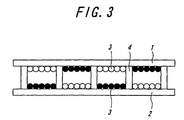
- Fig. 3 is a schematic view explaining a structure of the image display device.
- the image display device comprises opposed substrate 1 and substrate 2 and particles 3, and partition walls 4 are arranged according to need.
- At least one of the substrate 1 and 2 is a transparent substrate through which a color of the particles can be observed from outside of the device, and it is preferred to use a material having the high transmission factor of visible light and an excellent heat resistance.
- the image display device whether flexibility is necessary or not is suitably selected in accordance with its use. For example, it is preferred to use a material having flexibility for the use of electronic-paper and so on, and it is preferred to use a material having no flexibility for the use of a display of portable device such as mobile phone, PDA, laptop computer and so on.
- the substrate material examples include polymer sheets such as polyethylene terephthalate, polyether sulfone, polyethylene, or polycarbonate, and inorganic sheets such as glass, quartz or so.
- the thickness of the substrate is preferably 2 to 5000 ⁇ m, more preferably 5 to 1000 ⁇ m.
- the thickness is too thin, it becomes difficult to maintain strength and distance uniformity between the substrates, and when the thickness is too thick, vividness and contrast as a display capability degrade, and in particular, flexibility in the case of using for an electronic-paper deteriorates.
- an electrode may be arranged on the substrate according to need.
- the each particle charged in a predetermined characteristic and having a color is pulled in or rebounds with respect to the substrate by means of an electric field generated by applying an electrostatic latent image on an outer surface of the substrate. Then, the particle aligned in accordance with the electrostatic latent image is observed from outside of the display device through the transparent substrate.
- the electrostatic latent image mentioned above can be generated for example by a method wherein an electrostatic latent image generated in a known electrophotography system using an electrophotography photo-conductor is transferred and formed on the substrate of the image display device according to the invention, or, by a method wherein an electrostatic latent image is directly formed on the substrate by an ion flow.
- the powder charged in a predetermined characteristic and having a color is pulled in or rebounds with respect to the substrate by means of an electric field generated on respective electrodes formed on the substrate by applying an outer voltage thereto. Then, the powder aligned in accordance with the electrostatic latent image is observed from outside of the display device through the transparent substrate.
- the electrode may be formed of electroconductive materials which are transparent and having pattern formation capability.
- electroconductive materials metals such as aluminum, silver, nickel, copper, and gold, or transparent electroconductive metal oxides such as ITO, electroconductive tin oxide, and electroconductive zinc oxide formed in the shape of thin film by sputtering method, vacuum vapor deposition method, CVD (Chemical Vapor Deposition) method, and coating method, or coated materials obtained by applying the mixed solution of an electroconductive agent with a solvent or a synthetic resin binder are used.
- the electroconductive materials include cationic polyelectrolyte such as benzyltrimethylammonium chloride, tetrabutylammonium perchlorate, and so on, anionic polyelectrolyte such as polystyrenesulfonate, polyacrylate, and so on, or electroconductive fine powders of zinc oxide, tin oxide, or indium oxide.
- the thickness of the electrode may be suitable unless the electroconductivity is absent or any hindrance exists in optical transparency, and it is preferable to be 3 to 1000 nm, more preferable to be 5 to 400 nm.
- the foregoing transparent electrode materials can be employed as the opposed electrode, however, non-transparent electrode materials such as aluminum, silver, nickel, copper, and gold can be also employed.
- the applied outer voltage may be superimposed with a direct current or an alternate current.
- an insulation coating layer is formed on the electrode so as not to reduce charges of the charged particles. It is particularly preferred to form this coating layer by a resin having positive electrostatic property for the negatively charged particles and by a resin having negative electrostatic property for the positively charged particles, since the charges of the particles are difficult to be reduced.
- partition walls it is preferable to form partition walls around each display element.
- the partition walls may be formed in two parallel directions. By this structure, unnecessary particles movement in the direction parallel with the substrate is prevented. Further, durability, repeatability and memory retention are assisted. At the same time, the distance between the substrates is made uniform as reinforcing the strength of an image display panel.
- the formation method of the partition walls is not particularly restricted, however, a screen printing method wherein pastes are overlapped by coating repeatedly on a predetermined position by screen plate; a sandblast method wherein partition materials are painted with a desired thickness entirely over the substrate and then after coating resist pattern on the partition materials which is wanted to be left as a partition, jetting abrasive to cut and remove partition materials aside from the partition part; lift-off method (additive method) wherein a resist pattern is formed on the substrate using photopolymer, and then after burying paste into a resist recess, removing the resist; photosensitive paste method wherein the photosensitive resin composition containing the partition materials is applied over the substrate and then obtaining a desired pattern by exposure & developing; and mold formation method wherein paste containing the partition materials is applied over the substrate and then forming a partition by compression bonding & pressure forming the dies having rugged structure; and so on are adopted. Further, modifying the mold formation method, relief embossing method wherein a relief pattern provided by
- the particles it is preferred to use spherical particles due to its fluidity.
- the average particle diameter d(0.5) is preferable to be 0.1 to 50 ⁇ m, particularly to be 1 to 30 ⁇ m.
- the average particle diameter is less than this range, charge density of the particles will be so large that an imaging force to an electrode and a substrate becomes too strong; resulting in poor following ability at the inversion of its electric field, although the memory characteristic is favorable.
- the average particle diameter exceeds this range, the following ability is favorable, but the memory characteristic will degrade.
- the method for charging the particles negatively or positively is not particularly limited, a corona discharge method, an electrode injection-charge method, a friction charge method and so on are employable.
- the absolute value of the difference between the surface charge densities of the particles, which are measured by a blow-off method using a carrier is 5 - 150 ⁇ C/g as the absolute value.
- the absolute value of the surface charge density is less than this range, response speed to the change of an electric field will be late, and the memory property degrades.
- the absolute value of the surface charge density exceeds this range, image force for the electrode or the substrate will be so strong that the memory property will be favorable, but following ability will be poor in the case where the electric field is inverted.
- insulating particles with the volume specific resistance of 1 ⁇ 10 10 ⁇ cm or greater are preferable, and in particular, insulating particles with the volume specific resistance of 1 ⁇ 10 12 ⁇ cm or greater are more preferable.
- the feature of the invention is to use the particles for the image display having micro-irregularity on their surfaces. Since the micro-irregularity is arranged on the surface of the each particle, the following properties can be obtained.
- micro-irregularity is arranged on the surface of the each particle, a specific surface area per single particle can be increased. Therefore, chargeable sites are increased, and thus it is possible to obtain the particle having a sufficient electrostatic property. Moreover, the micro-irregularity causes a charge concentration at its portion, and thus it is possible to obtain the each particle having a more sufficient electrostatic property.
- micro-irregularity is arranged on the surface of the each particle, an incident light causes a irregular reflection, and thus the particle shows a white color when viewing.
- a specific surface area per each particle is increased by arranging the micro-irregularity on the surface of the each particle, but it is preferred that a product of a specific surface area S (m 2 /g) and an average particle diameter d(0.5) ( ⁇ m) of the particle: (S ⁇ d(0.5)) is 10 or more.
- the average particle diameter d(0.5) is obtained from the particle diameter distribution and means a value of the particle diameter expressed by ⁇ m wherein an amount of the particles having the particle diameter larger than or smaller than this value is 50 %.
- the particle diameter distribution and the average particle diameter mentioned above can be measured by means of a laser diffraction/scattering method.
- a laser light is incident upon the particles to be measured, a light intensity distribution pattern due to a diffraction / scattering light occurs spatially.
- This light intensity distribution pattern corresponds to the particle size, and thus it is possible to measure the particle diameter and the particle diameter distribution.
- the average particle diameter and the particle diameter distribution are obtained by a volume standard distribution.
- the average particle diameter and the particle diameter distribution can be measured by means of a measuring apparatus Mastersizer 2000 (Malvern Instruments Ltd.) wherein the particles setting in a nitrogen gas flow are calculated by an installed analysis software (which is based on a volume standard distribution due to Mie's theory).
- the method for arranging the micro-irregularity on the surface of the each particle is not particularly limited, and, for example, the following methods can be used.
- This treatment is performed by adding the child particles in a solution obtained by dissolving the charge control agent into the solvent, separating the child particles by means of a filtration and drying the filtered child particles.
- the child particles use is made of minute particles of metal oxide such as silica, titanium oxide. If a surface treatment is performed with respect to the minute particles by using the charge control agent, the charge control agent is fixed to each surface of the minute particles to show a white color, and it is possible to charge the particles in a desired property.
- metal oxide such as silica, titanium oxide.
- the charge control agent used for adhering the child particles on each surface of the mother particles is not limited if it is soluble in a solvent and its charge can be controlled, and thus any charge control agent available in the market may be preferably used.
- nigrosine compound resin acid modified azine
- resin acid modified azine compound the fourth grade ammonium salt
- salicylic acid metal complex phenol condensate
- metal-containing azo dye metal-containing azo dye
- triphenylmethane derivative use is made of nigrosine compound, resin acid modified azine, resin acid modified azine compound, the fourth grade ammonium salt, salicylic acid metal complex, phenol condensate, metal-containing azo dye, and triphenylmethane derivative.
- negative charge control agent such as salicylic acid metal complex, metal-containing azo dye, oil-soluble dye of metal-containing (containing a metal ion or a metal atom), the fourth grade ammonium salt-based compound, calixarene compound, boron-containing compound (benzyl acid boron complex), and nitroimidazole derivative.
- positive charge control agent include nigrosine dye, triphenylmethane compound, the fourth grade ammonium salt compound, polyamine resin, imidazole derivatives, etc.
- charge control agent use is made of nitrogen-containing circular compound such as pyridine, and so on, and these derivates or salts; and resins containing various organic pigments, fluorine, chlorine, nitrogen, etc.
- the solvent use is made of any solvent if it dissolves the charge control agent and shows no expansion and no dissolution of the minute particles, and normally it is preferred to use alcohol.
- the treatment method is performed by adding 0.1 - 10 % of the charge control agnet in the solvent, and agitating and dissolving them by means of a mixer and so on.
- the thus obtained solvent is subjected to a filtration so as to remove an undissolved component, and the minute particles is added in the filtered solvent which is further agitated by means of the mixer and so on.
- the minute particles treated by the filtration is picked up from the mixed solution and the picked-up minute particles is dried, so that the particle for the image display can be obtained.
- the charge control agent and coloring agent can be used at the same time.
- a coloring agent various kinds of organic or inorganic pigments or dye as will be described below are employable.
- black pigments examples include carbon black, copper oxide, manganese dioxide, aniline black, and activate carbon.
- yellow pigments include chrome yellow, zinc chromate, cadmium yellow, yellow iron oxide, mineral first yellow, nickel titanium yellow, navel orange yellow, naphthol yellow S, hanzayellow G, hanzayellow 10G, benzidine yellow G, benzidine yellow GR, quinoline yellow lake, permanent yellow NCG, and tartrazinelake.
- orange pigments examples include red chrome yellow, molybdenum orange, permanent orange GTR, pyrazolone orange, Balkan orange, Indanthrene brilliant orange RK, benzidine orange G, and Indanthrene brilliant orange GK.
- red pigments examples include red oxide, cadmium red, diachylon, mercury sulfide, cadmium, permanent red 4R, lithol red, pyrazolone red, watching red, calcium salt, lake red D, brilliant carmine 6B, eosin lake, rhodamine lake B, alizarin lake, and brilliant carmine 3B.
- purple pigments examples include manganese purple, first violet B, and methyl violet lake.
- blue pigments include Berlin blue, cobalt blue, alkali blue lake, Victoria blue lake, phthalocyanine blue, metal-free phthalocyanine blue, partially chlorinated phthalocyanine blue, first sky blue, and Indanthrene blue BC.
- green pigments examples include chrome green, chromium oxide, pigment green B, Malachite green lake, and final yellow green G.
- extenders examples include baryta powder, barium carbonate, clay, silica, white carbon, talc, and alumina white. Furthermore, there are Nigrosine, Methylene Blue, rose bengal, quinoline yellow, and ultramarine blue as various dyes such as basic dye, acidic dye, dispersion dye, direct dye, etc. These coloring agents may be used alone or in combination of two or more kinds thereof.
- the thus surface-treated minute particles (child particles) are fixed to the each mother particle as a core, and the electrostatic property applying and the coloring can be performed.
- the fixing method use may be made of a wet-type treatment method in which the child particles are coated on each surface of the mother particles together with binder resin.
- this wet-type treatment method it is necessary to select the solvent so as to prevent a re-dissolving of the charge control agent. Therefore, it is preferred to fix the child particles to the each mother particle by using a dry-type treatment method from the viewpoint of simplicity.
- Hybridizer Nara Machinery Co., Ltd.
- MechanoFusion Hosokawa Micron Co., Ltd.
- the ratio (d 1 /d 2 ) between the average particle diameter d 1 of the mother particles and the average particle diameter d 2 of the child particles is 10 or more.
- the ratio d 1 /d 2 is normally 100 or less. If the ratio d 1 /d 2 is less than 10 (that is, d 2 is larger), the number of the child particles to be fixed becomes smaller, and thus it is not possible to obtain the effects of the present invention.
- the mother particles may be preferably a circular shape and can be produced by performing the polymerization from monomer. Moreover, according to need, a classifying operation is performed for controlling the particle size. Further, in addition to this, the particle can be obtained by crashing and classifying the resin.
- the resin include urethane resin, urea resin, acrylic resin, polyester resin, acryl urethane resin, acryl urethane silicone resin, acryl urethane fluorocarbon polymers, acryl fluorocarbon polymers, silicone resin, acryl silicone resin, epoxy resin, polystyrene resin, styrene acrylic resin, polyolefin resin, butyral resin, vinylidene chloride resin, melamine resin, phenolic resin, fluorocarbon polymers, polycarbonate resin, polysulfon resin, polyether resin, and polyamide resin.
- acryl urethane resin for the purpose of controlling the attaching force with the substrate, acryl urethane resin, acryl silicone resin, acryl fluorocarbon polymers, acryl urethane silicone resin, acryl urethane fluorocarbon polymers, fluorocarbon polymers, silicone resin are particularly preferable. Two kinds or more of these may be mixed and used.
- the distance between the transparent substrate and the opposed substrate is suitably adjusted in a manner where the particles can move and maintain the contrast of image display; however, it is adjusted usually within 10 to 5000 ⁇ m, preferably within 30 to 500 ⁇ m.
- the volume population of the particles existing in the space between the faced substrates is preferable to be 10 to 80%, more preferable to be 10 to 70%.
- the image display device is applicable to the image display unit for mobile equipments such as notebook personal computers, PDAs, cellular phones and so on; to the electric-paper for electric book, electric-newspaper and so on; to the bulletin boards such as signboards, posters, blackboards and so on; and to the image display unit for electric calculator, home electric application products, auto supplies and so on.
- Respective particle was set in an apparatus for measuring a particle diameter distribution (Mastersizer2000, Malvern instruments Ltd.), and the particle diameter distribution was measured. Then, by using the attached analysis software, the average particle diameter d(0.5) ( ⁇ m), which was a value of the particle diameter expressed by ⁇ m wherein an amount of the particles having the particle diameter larger than or smaller than this value was 50 %, was determined.
- the blow-off method a mixture of the particles and the carriers are placed into a cylindrical container with nets at both ends, and high-pressure gas is blown from the one end to separate the particles and the carriers, and then only the particles are blew off from the mesh of the net.
- TB-200 As a blow-off powder charge amount measuring instrument, TB-200 produced by Toshiba Chemical Co., Ltd. was used. Two kinds of positively chargeable and negatively chargeable carrier-particles were employed as the carriers, and charge density per unit area (unit: ⁇ C/m 2 ) was measured in each case. Namely, F963-2535 available from Powder TEC Co., Ltd. was employed as a positive chargeable carrier-particle (the carrier whose opponent is positively charged and itself tends to be negative) and F921-2535 available from Powder TEC Co., Ltd. was employed as negatively chargeable carrier-particle (the carrier whose opponent is negatively charged and itself tends to be positive). The surface charge density of the particles was obtained from the measured charge amount, the average particle diameter and specific gravity of the particles measured separately.
- the specific gravity was measured with the use of a hydrometer produced by Shimadzu Seisakusho Ltd. (brand name: Multi volume Density Meter H1305).
- the black/white display was repeated by repeatedly inversing a potential of 500 V applied to the assembled display device.
- the estimation of the display function was performed by measuring displays of white color and black color by using a reflection image densitometer (RD918, Macbeth Co., Ltd.).
- unevenness at overall surface display was determined on the basis of the following standard.
- white color particles use was made of particles in which 0.2 wt% of hydrophobic silica (H3004, Hoechst Japan Ltd.) was added in a porous polymethyl methacrylate particles (MBP8, SEKISUI PLASTICS CO., LTD, the average particle diameter d(0.5) of 6.1 ⁇ m).
- hydrophobic silica H3004, Hoechst Japan Ltd.
- MBP8 porous polymethyl methacrylate particles
- black color particles use was made of a circular polymethyl methacrylate particles (Techpolymer MBX-5B, SEKISUI PLASTICS CO., LTD., the average particle diameter d(0.5) of 5.6 ⁇ m).
- the display device was produced as follows. That is, a pair of glass substrates, on which indium oxide electrode having a thickness of about 500 ⁇ (thickness: 50 nm), was assembled in such a manner that an interval between the substrates was controlled to be 100 ⁇ m by using spacers. Then, the white color particles and the black color particles mentioned above were filled in the space between the glass substrates, and peripheral portions of the glass substrates were connected by epoxy adhesive, so that the display device was produced. It should be noted that the mixing rate of the white color particles and the black color particles was controlled to be even, and the filling rate of theses particles between the glass substrates was controlled to be 50 vol%. The estimation results of the particles properties and the display functions are shown in Table 1.
- the image display device was produced in the same manner as that of the example 1, except that a circular polymethyl the methacrylate particle (MBX8, SEKISUI PLASTICS CO., LTD., the average particle diameter d(0.5) of 5.6 ⁇ m) was used as the white color particles instead of the porous polymethyl methacrylate particles (MBP8, SEKISUI PLASTICS CO., LTD., the average particle diameter d(0.5) of 6.1 ⁇ m).
- a circular polymethyl the methacrylate particle MBX8, SEKISUI PLASTICS CO., LTD., the average particle diameter d(0.5) of 5.6 ⁇ m
- MBP8 porous polymethyl methacrylate particles
- Example 1 Comparative Example 1 (White particles) Material MBP8 MBX8 Specific surface area (m 2 -g) 85 0.8 Average particle diameter d(0.5)( ⁇ m) 6.1 5.6 S ⁇ d(0.5) 518.5 4.48 Color White Clear Surface charge density ( ⁇ C/m 2 ) 48 33 (Black particles) Material MBX-5B MBX-5B Average particle diameter d(0.5)( ⁇ m) 5.6 5.6 Estimation of display particles Image displaying Overall white displaying (A) 0.45 0.75 Overall black displaying (B) 1.4 1.4 Contrast ratio (B/A) 3.1 1.9 Unevenness at overall displaying ⁇ ⁇ White color visibility ⁇ ⁇
- the present invention relates to particles for image displaying used in an image display device, in which one or more kind of particles are sealed between opposed substrates, at least one substrate being transparent, and, in which the particles are made to fly and move so as to display an image, characterized in that each particle has a micro-irregularity at its surface.
- the particle for the image display mentioned above since the particle for the image display mentioned above is used, it is possible to obtain the image, which can achieve a low electrostatic property, sufficiently apply an electrostatic property to the particles and stably obtain an excellent image having a sufficient contrast.
Landscapes
- Physics & Mathematics (AREA)
- Nonlinear Science (AREA)
- General Physics & Mathematics (AREA)
- Optics & Photonics (AREA)
- Electrochromic Elements, Electrophoresis, Or Variable Reflection Or Absorption Elements (AREA)
Applications Claiming Priority (5)
| Application Number | Priority Date | Filing Date | Title |
|---|---|---|---|
| JP2002125605 | 2002-04-26 | ||
| JP2002125605 | 2002-04-26 | ||
| JP2002307765 | 2002-10-23 | ||
| JP2002307765 | 2002-10-23 | ||
| PCT/JP2003/004923 WO2003091799A1 (en) | 2002-04-26 | 2003-04-17 | Particle for image display and its apparatus |
Publications (3)
| Publication Number | Publication Date |
|---|---|
| EP1500971A1 true EP1500971A1 (de) | 2005-01-26 |
| EP1500971A4 EP1500971A4 (de) | 2006-12-27 |
| EP1500971B1 EP1500971B1 (de) | 2010-01-13 |
Family
ID=29272360
Family Applications (1)
| Application Number | Title | Priority Date | Filing Date |
|---|---|---|---|
| EP03719124A Expired - Lifetime EP1500971B1 (de) | 2002-04-26 | 2003-04-17 | Methode zur Herstellung eines sphärischen Partikels zur Bildanzeige |
Country Status (7)
| Country | Link |
|---|---|
| US (1) | US7646530B2 (de) |
| EP (1) | EP1500971B1 (de) |
| JP (1) | JPWO2003091799A1 (de) |
| CN (1) | CN1324392C (de) |
| AU (1) | AU2003235215A1 (de) |
| DE (1) | DE60330959D1 (de) |
| WO (1) | WO2003091799A1 (de) |
Cited By (48)
| Publication number | Priority date | Publication date | Assignee | Title |
|---|---|---|---|---|
| US7034783B2 (en) | 2003-08-19 | 2006-04-25 | E Ink Corporation | Method for controlling electro-optic display |
| US7075703B2 (en) | 2004-01-16 | 2006-07-11 | E Ink Corporation | Process for sealing electro-optic displays |
| US7116466B2 (en) | 2004-07-27 | 2006-10-03 | E Ink Corporation | Electro-optic displays |
| US7119759B2 (en) | 1999-05-03 | 2006-10-10 | E Ink Corporation | Machine-readable displays |
| US7119772B2 (en) | 1999-04-30 | 2006-10-10 | E Ink Corporation | Methods for driving bistable electro-optic displays, and apparatus for use therein |
| US7173752B2 (en) | 2003-11-05 | 2007-02-06 | E Ink Corporation | Electro-optic displays, and materials for use therein |
| US7193625B2 (en) | 1999-04-30 | 2007-03-20 | E Ink Corporation | Methods for driving electro-optic displays, and apparatus for use therein |
| US7206119B2 (en) | 2003-12-31 | 2007-04-17 | E Ink Corporation | Electro-optic displays, and method for driving same |
| US7230751B2 (en) | 2005-01-26 | 2007-06-12 | E Ink Corporation | Electrophoretic displays using gaseous fluids |
| WO2007104003A2 (en) | 2006-03-08 | 2007-09-13 | E Ink Corporation | Methods for production of electro-optic displays |
| US7312794B2 (en) | 1999-04-30 | 2007-12-25 | E Ink Corporation | Methods for driving electro-optic displays, and apparatus for use therein |
| US7327511B2 (en) | 2004-03-23 | 2008-02-05 | E Ink Corporation | Light modulators |
| US7388572B2 (en) | 2004-02-27 | 2008-06-17 | E Ink Corporation | Backplanes for electro-optic displays |
| US7411719B2 (en) | 1995-07-20 | 2008-08-12 | E Ink Corporation | Electrophoretic medium and process for the production thereof |
| US7453445B2 (en) | 2004-08-13 | 2008-11-18 | E Ink Corproation | Methods for driving electro-optic displays |
| US7492339B2 (en) | 2004-03-26 | 2009-02-17 | E Ink Corporation | Methods for driving bistable electro-optic displays |
| US7528822B2 (en) | 2001-11-20 | 2009-05-05 | E Ink Corporation | Methods for driving electro-optic displays |
| EP2309322A1 (de) | 2006-09-22 | 2011-04-13 | E-Ink Corporation | Elektrooptische Anzeige und Materialien zur Verwendung darin |
| US7952557B2 (en) | 2001-11-20 | 2011-05-31 | E Ink Corporation | Methods and apparatus for driving electro-optic displays |
| US8009348B2 (en) | 1999-05-03 | 2011-08-30 | E Ink Corporation | Machine-readable displays |
| US8125501B2 (en) | 2001-11-20 | 2012-02-28 | E Ink Corporation | Voltage modulated driver circuits for electro-optic displays |
| US8174490B2 (en) | 2003-06-30 | 2012-05-08 | E Ink Corporation | Methods for driving electrophoretic displays |
| EP2487540A1 (de) | 2006-09-18 | 2012-08-15 | E-Ink Corporation | Elektrooptische Farbanzeigen |
| EP2546693A2 (de) | 2006-12-19 | 2013-01-16 | E Ink Corporation | Elektro-optische Anzeige mit Kantensiegel |
| EP2555182A1 (de) | 2007-02-02 | 2013-02-06 | E Ink Corporation | Elektrophoretische Anzeige mit transparenter Elektrode und damit verbundenem Leite |
| US8558783B2 (en) | 2001-11-20 | 2013-10-15 | E Ink Corporation | Electro-optic displays with reduced remnant voltage |
| US8593396B2 (en) | 2001-11-20 | 2013-11-26 | E Ink Corporation | Methods and apparatus for driving electro-optic displays |
| EP2711770A2 (de) | 2005-10-18 | 2014-03-26 | E Ink Corporation | Komponenten für elektrooptische Anzeigen |
| US8928562B2 (en) | 2003-11-25 | 2015-01-06 | E Ink Corporation | Electro-optic displays, and methods for driving same |
| US9412314B2 (en) | 2001-11-20 | 2016-08-09 | E Ink Corporation | Methods for driving electro-optic displays |
| US9530363B2 (en) | 2001-11-20 | 2016-12-27 | E Ink Corporation | Methods and apparatus for driving electro-optic displays |
| US9620067B2 (en) | 2003-03-31 | 2017-04-11 | E Ink Corporation | Methods for driving electro-optic displays |
| US9672766B2 (en) | 2003-03-31 | 2017-06-06 | E Ink Corporation | Methods for driving electro-optic displays |
| EP3220383A1 (de) | 2012-02-01 | 2017-09-20 | E Ink Corporation | Verfahren zur ansteuerung elektrooptischer anzeigen |
| US9779671B2 (en) | 2012-05-31 | 2017-10-03 | E Ink Corporation | Image display medium driving device, image display apparatus, driving program, and computer-readable medium |
| US9841653B2 (en) | 2007-03-06 | 2017-12-12 | E Ink Corporation | Materials for use in electrophoretic displays |
| US9966018B2 (en) | 2002-06-13 | 2018-05-08 | E Ink Corporation | Methods for driving electro-optic displays |
| US10331005B2 (en) | 2002-10-16 | 2019-06-25 | E Ink Corporation | Electrophoretic displays |
| EP3505585A1 (de) | 2007-11-14 | 2019-07-03 | E Ink Corporation | Haftstoffe und bindestoffe für elektrooptische anordnungen |
| US10726798B2 (en) | 2003-03-31 | 2020-07-28 | E Ink Corporation | Methods for operating electro-optic displays |
| US11250794B2 (en) | 2004-07-27 | 2022-02-15 | E Ink Corporation | Methods for driving electrophoretic displays using dielectrophoretic forces |
| EP4156165A2 (de) | 2013-07-31 | 2023-03-29 | E Ink Corporation | Verfahren zur ansteuerung elektrooptischer anzeigen |
| WO2023164078A1 (en) | 2022-02-25 | 2023-08-31 | E Ink Corporation | Electro-optic displays with edge seal components and methods of making the same |
| WO2023200859A1 (en) | 2022-04-13 | 2023-10-19 | E Ink Corporation | Display material including patterned areas of encapsulated electrophoretic media |
| WO2023211699A1 (en) | 2022-04-27 | 2023-11-02 | E Ink Corporation | Electro-optic display stacks with segmented electrodes and methods of making the same |
| WO2025034396A1 (en) | 2023-08-08 | 2025-02-13 | E Ink Corporation | Backplanes for segmented electro-optic displays and methods of manufacturing same |
| WO2025096239A1 (en) | 2023-10-30 | 2025-05-08 | E Ink Corporation | Electro-optic display with an electro-optic material layer having a binder comprising a polymer with a quaternary ammonium group and a method for manufacturing the same |
| WO2025155412A1 (en) | 2024-01-19 | 2025-07-24 | E Ink Corporation | Flexible segmented electro-optic displays and methods of manufacture |
Families Citing this family (76)
| Publication number | Priority date | Publication date | Assignee | Title |
|---|---|---|---|---|
| US7583251B2 (en) | 1995-07-20 | 2009-09-01 | E Ink Corporation | Dielectrophoretic displays |
| US7999787B2 (en) | 1995-07-20 | 2011-08-16 | E Ink Corporation | Methods for driving electrophoretic displays using dielectrophoretic forces |
| US7848006B2 (en) * | 1995-07-20 | 2010-12-07 | E Ink Corporation | Electrophoretic displays with controlled amounts of pigment |
| US8040594B2 (en) | 1997-08-28 | 2011-10-18 | E Ink Corporation | Multi-color electrophoretic displays |
| DE69920228T2 (de) | 1998-07-08 | 2005-01-27 | E-Ink Corp., Cambridge | Verfahren zur verbesserung der farbwiedergabe in elektrophoretischen vorrichtungen, welche mikrokapseln verwenden |
| US8115729B2 (en) | 1999-05-03 | 2012-02-14 | E Ink Corporation | Electrophoretic display element with filler particles |
| US7030854B2 (en) | 2001-03-13 | 2006-04-18 | E Ink Corporation | Apparatus for displaying drawings |
| US7679814B2 (en) | 2001-04-02 | 2010-03-16 | E Ink Corporation | Materials for use in electrophoretic displays |
| US8390918B2 (en) * | 2001-04-02 | 2013-03-05 | E Ink Corporation | Electrophoretic displays with controlled amounts of pigment |
| US7535624B2 (en) * | 2001-07-09 | 2009-05-19 | E Ink Corporation | Electro-optic display and materials for use therein |
| US6982178B2 (en) * | 2002-06-10 | 2006-01-03 | E Ink Corporation | Components and methods for use in electro-optic displays |
| US7223672B2 (en) * | 2002-04-24 | 2007-05-29 | E Ink Corporation | Processes for forming backplanes for electro-optic displays |
| US7554712B2 (en) | 2005-06-23 | 2009-06-30 | E Ink Corporation | Edge seals for, and processes for assembly of, electro-optic displays |
| US7583427B2 (en) * | 2002-06-10 | 2009-09-01 | E Ink Corporation | Components and methods for use in electro-optic displays |
| US7843621B2 (en) | 2002-06-10 | 2010-11-30 | E Ink Corporation | Components and testing methods for use in the production of electro-optic displays |
| US8363299B2 (en) | 2002-06-10 | 2013-01-29 | E Ink Corporation | Electro-optic displays, and processes for the production thereof |
| US8049947B2 (en) * | 2002-06-10 | 2011-11-01 | E Ink Corporation | Components and methods for use in electro-optic displays |
| CN101109885B (zh) | 2002-09-03 | 2012-06-13 | 伊英克公司 | 电光显示器 |
| US7839564B2 (en) | 2002-09-03 | 2010-11-23 | E Ink Corporation | Components and methods for use in electro-optic displays |
| AU2003289452A1 (en) * | 2002-12-24 | 2004-07-22 | Bridgestone Corporation | Image display |
| US7910175B2 (en) * | 2003-03-25 | 2011-03-22 | E Ink Corporation | Processes for the production of electrophoretic displays |
| KR100550548B1 (ko) * | 2003-09-30 | 2006-02-10 | 엘지전자 주식회사 | 평판 디스플레이 패널의 형광막 형성장치 |
| US7551346B2 (en) * | 2003-11-05 | 2009-06-23 | E Ink Corporation | Electro-optic displays, and materials for use therein |
| US20110164301A1 (en) | 2003-11-05 | 2011-07-07 | E Ink Corporation | Electro-optic displays, and materials for use therein |
| US7672040B2 (en) * | 2003-11-05 | 2010-03-02 | E Ink Corporation | Electro-optic displays, and materials for use therein |
| US8177942B2 (en) * | 2003-11-05 | 2012-05-15 | E Ink Corporation | Electro-optic displays, and materials for use therein |
| US8289250B2 (en) * | 2004-03-31 | 2012-10-16 | E Ink Corporation | Methods for driving electro-optic displays |
| JPWO2006018982A1 (ja) * | 2004-08-19 | 2008-05-08 | 株式会社ブリヂストン | 情報表示装置 |
| JP4328309B2 (ja) * | 2004-12-14 | 2009-09-09 | 株式会社ブリヂストン | 表示媒体用粒子及びそれを用いた情報表示用パネル |
| KR101184614B1 (ko) * | 2005-03-01 | 2012-09-21 | 소켄 케미칼 앤드 엔지니어링 캄파니, 리미티드 | 다공성 단분산 입자 및 그 제조 방법 및 그 용도 |
| WO2006109648A1 (ja) * | 2005-04-06 | 2006-10-19 | Bridgestone Corporation | 情報表示用パネル |
| JP2006313340A (ja) * | 2005-04-07 | 2006-11-16 | Bridgestone Corp | 表示媒体用粒子及びそれを用いた情報表示用パネル |
| US20080043318A1 (en) * | 2005-10-18 | 2008-02-21 | E Ink Corporation | Color electro-optic displays, and processes for the production thereof |
| US7843624B2 (en) * | 2006-03-08 | 2010-11-30 | E Ink Corporation | Electro-optic displays, and materials and methods for production thereof |
| US8390301B2 (en) * | 2006-03-08 | 2013-03-05 | E Ink Corporation | Electro-optic displays, and materials and methods for production thereof |
| US8610988B2 (en) | 2006-03-09 | 2013-12-17 | E Ink Corporation | Electro-optic display with edge seal |
| US7952790B2 (en) * | 2006-03-22 | 2011-05-31 | E Ink Corporation | Electro-optic media produced using ink jet printing |
| US7903319B2 (en) * | 2006-07-11 | 2011-03-08 | E Ink Corporation | Electrophoretic medium and display with improved image stability |
| US8018640B2 (en) | 2006-07-13 | 2011-09-13 | E Ink Corporation | Particles for use in electrophoretic displays |
| US20080024429A1 (en) * | 2006-07-25 | 2008-01-31 | E Ink Corporation | Electrophoretic displays using gaseous fluids |
| US7492497B2 (en) | 2006-08-02 | 2009-02-17 | E Ink Corporation | Multi-layer light modulator |
| US8144386B2 (en) * | 2006-09-22 | 2012-03-27 | Bridgestone Corporation | Particles for display media and information display panel using same |
| US7986450B2 (en) | 2006-09-22 | 2011-07-26 | E Ink Corporation | Electro-optic display and materials for use therein |
| US7649666B2 (en) * | 2006-12-07 | 2010-01-19 | E Ink Corporation | Components and methods for use in electro-optic displays |
| CN101836167B (zh) * | 2007-01-22 | 2013-11-06 | 伊英克公司 | 用在电光显示器中的多层板 |
| US7688497B2 (en) | 2007-01-22 | 2010-03-30 | E Ink Corporation | Multi-layer sheet for use in electro-optic displays |
| WO2008144715A1 (en) * | 2007-05-21 | 2008-11-27 | E Ink Corporation | Methods for driving video electro-optic displays |
| US9199441B2 (en) | 2007-06-28 | 2015-12-01 | E Ink Corporation | Processes for the production of electro-optic displays, and color filters for use therein |
| US8034209B2 (en) * | 2007-06-29 | 2011-10-11 | E Ink Corporation | Electro-optic displays, and materials and methods for production thereof |
| US8902153B2 (en) | 2007-08-03 | 2014-12-02 | E Ink Corporation | Electro-optic displays, and processes for their production |
| WO2009117730A1 (en) * | 2008-03-21 | 2009-09-24 | E Ink Corporation | Electro-optic displays and color filters |
| KR101214877B1 (ko) | 2008-04-11 | 2012-12-24 | 이 잉크 코포레이션 | 전기-광학 디스플레이들을 구동시키기 위한 방법 |
| JP2010128075A (ja) * | 2008-11-26 | 2010-06-10 | Konica Minolta Business Technologies Inc | 画像表示装置用表示粒子および画像表示装置 |
| TWI484273B (zh) * | 2009-02-09 | 2015-05-11 | E Ink Corp | 電泳粒子 |
| US8098418B2 (en) | 2009-03-03 | 2012-01-17 | E. Ink Corporation | Electro-optic displays, and color filters for use therein |
| US8654436B1 (en) | 2009-10-30 | 2014-02-18 | E Ink Corporation | Particles for use in electrophoretic displays |
| WO2011097228A2 (en) | 2010-02-02 | 2011-08-11 | E Ink Corporation | Method for driving electro-optic displays |
| EP2553522B1 (de) | 2010-04-02 | 2016-03-23 | E-Ink Corporation | Elektrophoretische medien |
| TWI484275B (zh) | 2010-05-21 | 2015-05-11 | E Ink Corp | 光電顯示器及其驅動方法、微型空腔電泳顯示器 |
| US8797634B2 (en) | 2010-11-30 | 2014-08-05 | E Ink Corporation | Multi-color electrophoretic displays |
| JP6028373B2 (ja) * | 2012-04-05 | 2016-11-16 | セイコーエプソン株式会社 | 電気泳動粒子、電気泳動粒子の製造方法、電気泳動分散液、電気泳動シート、電気泳動装置および電子機器 |
| EP3254276A4 (de) | 2015-02-04 | 2018-07-11 | E Ink Corporation | Elektrooptische anzeigen mit reduzierter restspannung und zugehörige vorrichtung und verfahren |
| US10803813B2 (en) | 2015-09-16 | 2020-10-13 | E Ink Corporation | Apparatus and methods for driving displays |
| WO2017049020A1 (en) | 2015-09-16 | 2017-03-23 | E Ink Corporation | Apparatus and methods for driving displays |
| US11657774B2 (en) | 2015-09-16 | 2023-05-23 | E Ink Corporation | Apparatus and methods for driving displays |
| TWI631542B (zh) | 2015-11-18 | 2018-08-01 | 美商電子墨水股份有限公司 | 電光顯示器 |
| CN112313572B (zh) | 2018-06-28 | 2024-08-16 | 伊英克公司 | 用于可变透射电泳介质的驱动方法 |
| EP3966628B1 (de) | 2019-05-07 | 2025-04-23 | E Ink Corporation | Ansteuerverfahren für eine variable lichtübertragungsvorrichtung |
| GB2593150A (en) | 2020-03-05 | 2021-09-22 | Vlyte Ltd | A light modulator having bonded structures embedded in its viewing area |
| CN116324609A (zh) | 2020-07-22 | 2023-06-23 | 伊英克公司 | 包含集成的导电边缘密封件的电光装置和用于生产电光装置的方法 |
| CN117136168A (zh) * | 2021-03-31 | 2023-11-28 | 福吉米株式会社 | 板状焦磷酸钛及其制造方法 |
| WO2023049481A1 (en) | 2021-09-27 | 2023-03-30 | E Ink Corporation | Electrophoretic particle film having reduced diffraction in an open state |
| WO2025019101A1 (en) | 2023-07-18 | 2025-01-23 | E Ink Corporation | Switchable electrophoretic light modulator having reduced aperture diffraction |
| US20250116908A1 (en) | 2023-10-06 | 2025-04-10 | E Ink Corporation | Large-area electro-optic light modulator or display |
| WO2025101330A1 (en) | 2023-11-08 | 2025-05-15 | E Ink Corporation | Continuous photolithographic fabrication process for producing seamless microstructures used in electro-optic displays and light modulating films |
| US20250284171A1 (en) | 2024-03-06 | 2025-09-11 | E Ink Corporation | Electro-optic displays with color filter arrays for reducing visible texture patterns in displayed images |
Family Cites Families (12)
| Publication number | Priority date | Publication date | Assignee | Title |
|---|---|---|---|---|
| JPS63153525A (ja) * | 1986-12-17 | 1988-06-25 | Fuji Electric Co Ltd | エレクトロクロミツク表示素子 |
| JPH05173193A (ja) | 1991-12-25 | 1993-07-13 | Dainippon Printing Co Ltd | 電気泳動表示用の分散系およびその分散系を用いた電気泳動表示素子 |
| JP3277081B2 (ja) * | 1994-10-13 | 2002-04-22 | 株式会社東芝 | 異形樹脂粒子、樹脂粒子の異形化方法、及び異形樹脂粒子からなる電子写真用トナー |
| US6760086B2 (en) * | 1998-03-26 | 2004-07-06 | Tomoegawa Paper Co., Ltd. | Attachment film for electronic display device |
| JPH11297212A (ja) * | 1998-04-15 | 1999-10-29 | Hitachi Ltd | プラズマディスプレイ |
| AU1738700A (en) * | 1998-11-20 | 2000-06-13 | California Institute Of Technology | Slotted quantum well sensor |
| DE19927359A1 (de) * | 1999-06-16 | 2000-12-21 | Creavis Tech & Innovation Gmbh | Elektrophoretische Displays aus lichtstreuenden Trägermaterialien |
| JP4126851B2 (ja) | 1999-07-21 | 2008-07-30 | 富士ゼロックス株式会社 | 画像表示媒体、画像形成方法、及び画像形成装置 |
| US6774879B2 (en) * | 2000-06-09 | 2004-08-10 | Minolta Co., Ltd. | Reversible image display medium |
| JP4062864B2 (ja) | 2000-06-09 | 2008-03-19 | コニカミノルタホールディングス株式会社 | 可逆性画像表示媒体 |
| JP4061830B2 (ja) * | 2000-08-31 | 2008-03-19 | 富士ゼロックス株式会社 | 画像表示媒体 |
| EP1317517A1 (de) * | 2000-09-14 | 2003-06-11 | Dsm N.V. | Beschichtungszusammensetzungen für kunststoffsubstrate |
-
2003
- 2003-04-17 EP EP03719124A patent/EP1500971B1/de not_active Expired - Lifetime
- 2003-04-17 AU AU2003235215A patent/AU2003235215A1/en not_active Abandoned
- 2003-04-17 US US10/512,421 patent/US7646530B2/en not_active Expired - Fee Related
- 2003-04-17 DE DE60330959T patent/DE60330959D1/de not_active Expired - Lifetime
- 2003-04-17 JP JP2004500118A patent/JPWO2003091799A1/ja active Pending
- 2003-04-17 CN CNB038119609A patent/CN1324392C/zh not_active Expired - Fee Related
- 2003-04-17 WO PCT/JP2003/004923 patent/WO2003091799A1/ja not_active Ceased
Cited By (68)
| Publication number | Priority date | Publication date | Assignee | Title |
|---|---|---|---|---|
| US7848007B2 (en) | 1995-07-20 | 2010-12-07 | E Ink Corporation | Electrophoretic medium and process for the production thereof |
| US7411719B2 (en) | 1995-07-20 | 2008-08-12 | E Ink Corporation | Electrophoretic medium and process for the production thereof |
| US7688297B2 (en) | 1999-04-30 | 2010-03-30 | E Ink Corporation | Methods for driving bistable electro-optic displays, and apparatus for use therein |
| US7119772B2 (en) | 1999-04-30 | 2006-10-10 | E Ink Corporation | Methods for driving bistable electro-optic displays, and apparatus for use therein |
| US10319314B2 (en) | 1999-04-30 | 2019-06-11 | E Ink Corporation | Methods for driving electro-optic displays, and apparatus for use therein |
| US7193625B2 (en) | 1999-04-30 | 2007-03-20 | E Ink Corporation | Methods for driving electro-optic displays, and apparatus for use therein |
| US7733311B2 (en) | 1999-04-30 | 2010-06-08 | E Ink Corporation | Methods for driving bistable electro-optic displays, and apparatus for use therein |
| US7733335B2 (en) | 1999-04-30 | 2010-06-08 | E Ink Corporation | Methods for driving bistable electro-optic displays, and apparatus for use therein |
| US8558785B2 (en) | 1999-04-30 | 2013-10-15 | E Ink Corporation | Methods for driving bistable electro-optic displays, and apparatus for use therein |
| US7312794B2 (en) | 1999-04-30 | 2007-12-25 | E Ink Corporation | Methods for driving electro-optic displays, and apparatus for use therein |
| US10909936B2 (en) | 1999-04-30 | 2021-02-02 | E Ink Corporation | Methods for driving bistable electro-optic displays, and apparatus for use therein |
| US7119759B2 (en) | 1999-05-03 | 2006-10-10 | E Ink Corporation | Machine-readable displays |
| US8009348B2 (en) | 1999-05-03 | 2011-08-30 | E Ink Corporation | Machine-readable displays |
| US9886886B2 (en) | 2001-11-20 | 2018-02-06 | E Ink Corporation | Methods for driving electro-optic displays |
| US8558783B2 (en) | 2001-11-20 | 2013-10-15 | E Ink Corporation | Electro-optic displays with reduced remnant voltage |
| US8593396B2 (en) | 2001-11-20 | 2013-11-26 | E Ink Corporation | Methods and apparatus for driving electro-optic displays |
| US8125501B2 (en) | 2001-11-20 | 2012-02-28 | E Ink Corporation | Voltage modulated driver circuits for electro-optic displays |
| US9412314B2 (en) | 2001-11-20 | 2016-08-09 | E Ink Corporation | Methods for driving electro-optic displays |
| US7528822B2 (en) | 2001-11-20 | 2009-05-05 | E Ink Corporation | Methods for driving electro-optic displays |
| US7952557B2 (en) | 2001-11-20 | 2011-05-31 | E Ink Corporation | Methods and apparatus for driving electro-optic displays |
| US9530363B2 (en) | 2001-11-20 | 2016-12-27 | E Ink Corporation | Methods and apparatus for driving electro-optic displays |
| US9564088B2 (en) | 2001-11-20 | 2017-02-07 | E Ink Corporation | Electro-optic displays with reduced remnant voltage |
| US9881564B2 (en) | 2001-11-20 | 2018-01-30 | E Ink Corporation | Electro-optic displays with reduced remnant voltage |
| US9921422B2 (en) | 2002-06-10 | 2018-03-20 | E Ink Corporation | Electro-optic display with edge seal |
| US9612502B2 (en) | 2002-06-10 | 2017-04-04 | E Ink Corporation | Electro-optic display with edge seal |
| US9966018B2 (en) | 2002-06-13 | 2018-05-08 | E Ink Corporation | Methods for driving electro-optic displays |
| US10331005B2 (en) | 2002-10-16 | 2019-06-25 | E Ink Corporation | Electrophoretic displays |
| US9672766B2 (en) | 2003-03-31 | 2017-06-06 | E Ink Corporation | Methods for driving electro-optic displays |
| US9620067B2 (en) | 2003-03-31 | 2017-04-11 | E Ink Corporation | Methods for driving electro-optic displays |
| US10726798B2 (en) | 2003-03-31 | 2020-07-28 | E Ink Corporation | Methods for operating electro-optic displays |
| US8174490B2 (en) | 2003-06-30 | 2012-05-08 | E Ink Corporation | Methods for driving electrophoretic displays |
| US7545358B2 (en) | 2003-08-19 | 2009-06-09 | E Ink Corporation | Methods for controlling electro-optic displays |
| US7034783B2 (en) | 2003-08-19 | 2006-04-25 | E Ink Corporation | Method for controlling electro-optic display |
| US7173752B2 (en) | 2003-11-05 | 2007-02-06 | E Ink Corporation | Electro-optic displays, and materials for use therein |
| US7349148B2 (en) | 2003-11-05 | 2008-03-25 | E Ink Corporation | Electro-optic displays, and materials for use therein |
| US8928562B2 (en) | 2003-11-25 | 2015-01-06 | E Ink Corporation | Electro-optic displays, and methods for driving same |
| US9542895B2 (en) | 2003-11-25 | 2017-01-10 | E Ink Corporation | Electro-optic displays, and methods for driving same |
| US7206119B2 (en) | 2003-12-31 | 2007-04-17 | E Ink Corporation | Electro-optic displays, and method for driving same |
| US7075703B2 (en) | 2004-01-16 | 2006-07-11 | E Ink Corporation | Process for sealing electro-optic displays |
| US7388572B2 (en) | 2004-02-27 | 2008-06-17 | E Ink Corporation | Backplanes for electro-optic displays |
| US7327511B2 (en) | 2004-03-23 | 2008-02-05 | E Ink Corporation | Light modulators |
| US7492339B2 (en) | 2004-03-26 | 2009-02-17 | E Ink Corporation | Methods for driving bistable electro-optic displays |
| US11250794B2 (en) | 2004-07-27 | 2022-02-15 | E Ink Corporation | Methods for driving electrophoretic displays using dielectrophoretic forces |
| US7304787B2 (en) | 2004-07-27 | 2007-12-04 | E Ink Corporation | Electro-optic displays |
| US7116466B2 (en) | 2004-07-27 | 2006-10-03 | E Ink Corporation | Electro-optic displays |
| US7453445B2 (en) | 2004-08-13 | 2008-11-18 | E Ink Corproation | Methods for driving electro-optic displays |
| US7230751B2 (en) | 2005-01-26 | 2007-06-12 | E Ink Corporation | Electrophoretic displays using gaseous fluids |
| EP2711770A2 (de) | 2005-10-18 | 2014-03-26 | E Ink Corporation | Komponenten für elektrooptische Anzeigen |
| EP2309304A2 (de) | 2006-03-08 | 2011-04-13 | E-Ink Corporation | Verfahren zur Herstellung von elektrooptischen Anzeigen |
| EP2437114A1 (de) | 2006-03-08 | 2012-04-04 | E-Ink Corporation | Verfahren zur Herstellung von elektrooptischen Anzeigen |
| WO2007104003A2 (en) | 2006-03-08 | 2007-09-13 | E Ink Corporation | Methods for production of electro-optic displays |
| EP2487540A1 (de) | 2006-09-18 | 2012-08-15 | E-Ink Corporation | Elektrooptische Farbanzeigen |
| EP2309322A1 (de) | 2006-09-22 | 2011-04-13 | E-Ink Corporation | Elektrooptische Anzeige und Materialien zur Verwendung darin |
| EP2546693A2 (de) | 2006-12-19 | 2013-01-16 | E Ink Corporation | Elektro-optische Anzeige mit Kantensiegel |
| EP2555182A1 (de) | 2007-02-02 | 2013-02-06 | E Ink Corporation | Elektrophoretische Anzeige mit transparenter Elektrode und damit verbundenem Leite |
| US9841653B2 (en) | 2007-03-06 | 2017-12-12 | E Ink Corporation | Materials for use in electrophoretic displays |
| EP3505585A1 (de) | 2007-11-14 | 2019-07-03 | E Ink Corporation | Haftstoffe und bindestoffe für elektrooptische anordnungen |
| EP3220383A1 (de) | 2012-02-01 | 2017-09-20 | E Ink Corporation | Verfahren zur ansteuerung elektrooptischer anzeigen |
| EP3783597A1 (de) | 2012-02-01 | 2021-02-24 | E Ink Corporation | Verfahren zur ansteuerung elektrooptischer anzeigen |
| US9779671B2 (en) | 2012-05-31 | 2017-10-03 | E Ink Corporation | Image display medium driving device, image display apparatus, driving program, and computer-readable medium |
| EP4156165A2 (de) | 2013-07-31 | 2023-03-29 | E Ink Corporation | Verfahren zur ansteuerung elektrooptischer anzeigen |
| EP4156164A1 (de) | 2013-07-31 | 2023-03-29 | E Ink Corporation | Verfahren zur ansteuerung elektrooptischer anzeigen |
| WO2023164078A1 (en) | 2022-02-25 | 2023-08-31 | E Ink Corporation | Electro-optic displays with edge seal components and methods of making the same |
| WO2023200859A1 (en) | 2022-04-13 | 2023-10-19 | E Ink Corporation | Display material including patterned areas of encapsulated electrophoretic media |
| WO2023211699A1 (en) | 2022-04-27 | 2023-11-02 | E Ink Corporation | Electro-optic display stacks with segmented electrodes and methods of making the same |
| WO2025034396A1 (en) | 2023-08-08 | 2025-02-13 | E Ink Corporation | Backplanes for segmented electro-optic displays and methods of manufacturing same |
| WO2025096239A1 (en) | 2023-10-30 | 2025-05-08 | E Ink Corporation | Electro-optic display with an electro-optic material layer having a binder comprising a polymer with a quaternary ammonium group and a method for manufacturing the same |
| WO2025155412A1 (en) | 2024-01-19 | 2025-07-24 | E Ink Corporation | Flexible segmented electro-optic displays and methods of manufacture |
Also Published As
| Publication number | Publication date |
|---|---|
| US7646530B2 (en) | 2010-01-12 |
| DE60330959D1 (de) | 2010-03-04 |
| EP1500971A4 (de) | 2006-12-27 |
| JPWO2003091799A1 (ja) | 2005-09-02 |
| EP1500971B1 (de) | 2010-01-13 |
| AU2003235215A1 (en) | 2003-11-10 |
| CN1324392C (zh) | 2007-07-04 |
| US20060087718A1 (en) | 2006-04-27 |
| WO2003091799A1 (en) | 2003-11-06 |
| CN1656418A (zh) | 2005-08-17 |
Similar Documents
| Publication | Publication Date | Title |
|---|---|---|
| US7646530B2 (en) | Particle and device for image display | |
| US7646358B2 (en) | Image display device | |
| US7639417B2 (en) | White color particles for display media and information display device utilizing them | |
| US20060214906A1 (en) | Image display | |
| US20060087489A1 (en) | Image display | |
| US20050259068A1 (en) | Image display | |
| US7224510B2 (en) | Reversible image display sheet and image display | |
| EP1662305B1 (de) | Bildanzeigetafel-herstellungsverfahren | |
| US7580179B2 (en) | Method of manufacturing information display device | |
| US20070252793A1 (en) | Information Display Device | |
| US7483201B2 (en) | Particles for display media, information display panel and information display device, utilizing the particles for display media | |
| JP4614711B2 (ja) | 画像表示用パネルの製造方法 | |
| EP1855154A1 (de) | Teilchen für Anzeigemedien und Informationsanzeigetafel mit den Teilchen | |
| JP4614714B2 (ja) | 画像表示用パネルの製造方法 | |
| EP1843197A1 (de) | Partikel für Anzeigemedien und Informationsanzeigetafel mit diesen Partikeln | |
| JP5052104B2 (ja) | 表示媒体用粒子、情報表示用パネルおよび情報表示装置 | |
| JP4925606B2 (ja) | 情報表示用パネルの製造方法 | |
| JP2003255401A (ja) | 画像表示装置および方法 | |
| JP4763985B2 (ja) | 画像表示装置 | |
| JP4671642B2 (ja) | 画像表示用パネル及びその製造方法 | |
| JP2006058550A (ja) | 画像表示用パネル、その製造方法及び画像表示装置 | |
| JP2006293154A (ja) | 情報表示用パネルの製造方法および情報表示用パネル | |
| JP2003222912A (ja) | 画像表示装置および方法 | |
| JP2006039119A (ja) | 画像表示装置およびその製造方法 | |
| JP2008102231A (ja) | 表示媒体用粒子およびそれを用いた情報表示用パネル |
Legal Events
| Date | Code | Title | Description |
|---|---|---|---|
| PUAI | Public reference made under article 153(3) epc to a published international application that has entered the european phase |
Free format text: ORIGINAL CODE: 0009012 |
|
| 17P | Request for examination filed |
Effective date: 20041029 |
|
| AK | Designated contracting states |
Kind code of ref document: A1 Designated state(s): AT BE BG CH CY CZ DE DK EE ES FI FR GB GR HU IE IT LI LU MC NL PT RO SE SI SK TR |
|
| AX | Request for extension of the european patent |
Extension state: AL LT LV MK |
|
| RIN1 | Information on inventor provided before grant (corrected) |
Inventor name: KITANO, HAJIME Inventor name: TAKAGI, KOJI Inventor name: MURATA, KAZUYA Inventor name: NIHEI, NORIO Inventor name: YAKUSHIJI, GAKU Inventor name: KAWAGOE, TAKAHIRO Inventor name: MASUDA, YOSHITOMO |
|
| A4 | Supplementary search report drawn up and despatched |
Effective date: 20061123 |
|
| 17Q | First examination report despatched |
Effective date: 20070212 |
|
| RTI1 | Title (correction) |
Free format text: METHOD OF PRODUCING A SPHERICAL PARTICLE FOR IMAGE DISPLAY |
|
| GRAP | Despatch of communication of intention to grant a patent |
Free format text: ORIGINAL CODE: EPIDOSNIGR1 |
|
| GRAS | Grant fee paid |
Free format text: ORIGINAL CODE: EPIDOSNIGR3 |
|
| GRAA | (expected) grant |
Free format text: ORIGINAL CODE: 0009210 |
|
| AK | Designated contracting states |
Kind code of ref document: B1 Designated state(s): DE FR |
|
| REF | Corresponds to: |
Ref document number: 60330959 Country of ref document: DE Date of ref document: 20100304 Kind code of ref document: P |
|
| PLBE | No opposition filed within time limit |
Free format text: ORIGINAL CODE: 0009261 |
|
| STAA | Information on the status of an ep patent application or granted ep patent |
Free format text: STATUS: NO OPPOSITION FILED WITHIN TIME LIMIT |
|
| 26N | No opposition filed |
Effective date: 20101014 |
|
| REG | Reference to a national code |
Ref country code: DE Ref legal event code: R082 Ref document number: 60330959 Country of ref document: DE Representative=s name: MARKS & CLERK (LUXEMBOURG) LLP, LU |
|
| REG | Reference to a national code |
Ref country code: FR Ref legal event code: CA Effective date: 20140812 |
|
| REG | Reference to a national code |
Ref country code: DE Ref legal event code: R082 Ref document number: 60330959 Country of ref document: DE Representative=s name: MARKS & CLERK (LUXEMBOURG) LLP, LU Effective date: 20140828 Ref country code: DE Ref legal event code: R081 Ref document number: 60330959 Country of ref document: DE Owner name: BRIDGESTONE CORPORATION, JP Free format text: FORMER OWNER: BRIDGESTONE CORP., TOKIO/TOKYO, JP Effective date: 20140828 |
|
| REG | Reference to a national code |
Ref country code: FR Ref legal event code: PLFP Year of fee payment: 13 |
|
| PGFP | Annual fee paid to national office [announced via postgrant information from national office to epo] |
Ref country code: DE Payment date: 20150421 Year of fee payment: 13 |
|
| PGFP | Annual fee paid to national office [announced via postgrant information from national office to epo] |
Ref country code: FR Payment date: 20150421 Year of fee payment: 13 |
|
| REG | Reference to a national code |
Ref country code: DE Ref legal event code: R119 Ref document number: 60330959 Country of ref document: DE |
|
| REG | Reference to a national code |
Ref country code: FR Ref legal event code: ST Effective date: 20161230 |
|
| PG25 | Lapsed in a contracting state [announced via postgrant information from national office to epo] |
Ref country code: FR Free format text: LAPSE BECAUSE OF NON-PAYMENT OF DUE FEES Effective date: 20160502 Ref country code: DE Free format text: LAPSE BECAUSE OF NON-PAYMENT OF DUE FEES Effective date: 20161101 |