EP1500146B1 - Procede de fabrication de semi-conducteurs en couches minces a base de composes i-iii-vi(2), pour applications photovoltaiques - Google Patents
Procede de fabrication de semi-conducteurs en couches minces a base de composes i-iii-vi(2), pour applications photovoltaiques Download PDFInfo
- Publication number
- EP1500146B1 EP1500146B1 EP03747464.0A EP03747464A EP1500146B1 EP 1500146 B1 EP1500146 B1 EP 1500146B1 EP 03747464 A EP03747464 A EP 03747464A EP 1500146 B1 EP1500146 B1 EP 1500146B1
- Authority
- EP
- European Patent Office
- Prior art keywords
- layer
- iii
- annealing
- precursor
- composition
- Prior art date
- Legal status (The legal status is an assumption and is not a legal conclusion. Google has not performed a legal analysis and makes no representation as to the accuracy of the status listed.)
- Expired - Lifetime
Links
Images



Classifications
-
- H—ELECTRICITY
- H10—SEMICONDUCTOR DEVICES; ELECTRIC SOLID-STATE DEVICES NOT OTHERWISE PROVIDED FOR
- H10F—INORGANIC SEMICONDUCTOR DEVICES SENSITIVE TO INFRARED RADIATION, LIGHT, ELECTROMAGNETIC RADIATION OF SHORTER WAVELENGTH OR CORPUSCULAR RADIATION
- H10F77/00—Constructional details of devices covered by this subclass
- H10F77/10—Semiconductor bodies
- H10F77/12—Active materials
- H10F77/126—Active materials comprising only Group I-III-VI chalcopyrite materials, e.g. CuInSe2, CuGaSe2 or CuInGaSe2 [CIGS]
-
- H—ELECTRICITY
- H10—SEMICONDUCTOR DEVICES; ELECTRIC SOLID-STATE DEVICES NOT OTHERWISE PROVIDED FOR
- H10F—INORGANIC SEMICONDUCTOR DEVICES SENSITIVE TO INFRARED RADIATION, LIGHT, ELECTROMAGNETIC RADIATION OF SHORTER WAVELENGTH OR CORPUSCULAR RADIATION
- H10F71/00—Manufacture or treatment of devices covered by this subclass
- H10F71/128—Annealing
-
- H—ELECTRICITY
- H10—SEMICONDUCTOR DEVICES; ELECTRIC SOLID-STATE DEVICES NOT OTHERWISE PROVIDED FOR
- H10F—INORGANIC SEMICONDUCTOR DEVICES SENSITIVE TO INFRARED RADIATION, LIGHT, ELECTROMAGNETIC RADIATION OF SHORTER WAVELENGTH OR CORPUSCULAR RADIATION
- H10F71/00—Manufacture or treatment of devices covered by this subclass
- H10F71/131—Recrystallisation; Crystallization of amorphous or microcrystalline semiconductors
-
- Y—GENERAL TAGGING OF NEW TECHNOLOGICAL DEVELOPMENTS; GENERAL TAGGING OF CROSS-SECTIONAL TECHNOLOGIES SPANNING OVER SEVERAL SECTIONS OF THE IPC; TECHNICAL SUBJECTS COVERED BY FORMER USPC CROSS-REFERENCE ART COLLECTIONS [XRACs] AND DIGESTS
- Y02—TECHNOLOGIES OR APPLICATIONS FOR MITIGATION OR ADAPTATION AGAINST CLIMATE CHANGE
- Y02E—REDUCTION OF GREENHOUSE GAS [GHG] EMISSIONS, RELATED TO ENERGY GENERATION, TRANSMISSION OR DISTRIBUTION
- Y02E10/00—Energy generation through renewable energy sources
- Y02E10/50—Photovoltaic [PV] energy
- Y02E10/541—CuInSe2 material PV cells
-
- Y—GENERAL TAGGING OF NEW TECHNOLOGICAL DEVELOPMENTS; GENERAL TAGGING OF CROSS-SECTIONAL TECHNOLOGIES SPANNING OVER SEVERAL SECTIONS OF THE IPC; TECHNICAL SUBJECTS COVERED BY FORMER USPC CROSS-REFERENCE ART COLLECTIONS [XRACs] AND DIGESTS
- Y02—TECHNOLOGIES OR APPLICATIONS FOR MITIGATION OR ADAPTATION AGAINST CLIMATE CHANGE
- Y02P—CLIMATE CHANGE MITIGATION TECHNOLOGIES IN THE PRODUCTION OR PROCESSING OF GOODS
- Y02P70/00—Climate change mitigation technologies in the production process for final industrial or consumer products
- Y02P70/50—Manufacturing or production processes characterised by the final manufactured product
Definitions
- the present invention relates to the field of thin film deposition of semiconductors for photovoltaic applications.
- Thin layers of diselenide and / or disulfide of copper and indium and / or gallium (CIGS) are deposited on a substrate to make photovoltaic cells.
- Such compounds of general formula CuGa x In 1-x Se 2 -y S y (with x between 0 and 1 and between 0 and 2), are considered very promising and could constitute the next generation of solar cells. in thin layers.
- the CIGS semiconductor materials have a band gap (" gap ”) between 1.0 and 1.6 eV which allows a strong absorption of school radiation in the visible. Record conversion efficiencies greater than. 18%, were recently obtained on cells of small areas.
- the CIGS layers used for photovoltaic conversion must have a p-type semiconductor character and good charge transport properties. These charge transport properties are favored by good crystallinity. Thus, the CIGS compounds must be at least partially crystallized to have sufficient photovoltaic properties for their application to the manufacture of solar cells.
- the crystallized CIGS compounds have a crystallographic structure corresponding to the chalcopyrite or sphalerite system, depending on the deposition temperature.
- Thin layers of CIGS when deposited at low temperature (precursor deposition), are weakly crystalline, even amorphous, and thermal annealing of the layers must be performed to obtain an improvement of the crystallization of the CIGS and the properties satisfactory load transport.
- one of the constituent elements of CIGS in principle selenium Se is more volatile than the other elements. It is therefore difficult to obtain crystallized CIGS with the desired composition (close to stoichiometry I-III-VI 2 ) without adding selenium for annealing the precursor layer.
- the composition of the layers must have a slight difference at stoichiometry I-III-VI 2 , in favor of element VI.
- the prior art embodiments utilize annealing of the precursor deposits in the presence of an excess of selenium in the vapor phase.
- precursors means intermediate compounds whose physicochemical properties are distinct from those of CIS (or CIGS) and render them unfit for photovoltaic conversion. They are initially deposited in the form of a thin layer, this thin layer being then treated to form the desired deposit of CIGS.
- the document DE 19917758 A1 describes the manufacture of a CIS layer from a ternary deposition by electrochemistry. The supply of selenium in the annealing furnace is avoided by a very rapid heating annealing.
- U.S. 5,578,503 discloses a two-step process, which firstly provides a sputtering deposit (or " sputtering ”) , then a rapid annealing (lamps) of the precursors thus deposited.
- precursor elements Cu, In and Se are separately deposited in elemental form (Cu (0), In (0) and Se (0)) or in the form of binaries (such as In 2 Se 3 ).
- the structure initially deposited before annealing is essentially heterogeneous and is in the form of a multiplicity of successive layers (stacks of Cu 0 / In 0 / Se 0 or Cu 0 / In 2 Se 3 , or a combination of the two ) in the direction of the thickness of the layer.
- This mixture of precursors is then subjected to rapid annealing, including a rise in temperature followed by a step required to homogenize the CIS layer.
- the thin layer deposited by sputtering and of heterogeneous structure in sheets does not withstand, notably mechanically, abrupt climbs at temperature. Since the coefficient of temperature expansion of the layer is spatially inhomogeneous, peeling problems of this layer may appear during the annealing step. Such a method, although advantageous, is not yet completely satisfactory.
- the methods of deposition by evaporation or sputtering use sources that are commonly made up of elements pure, or possibly binary, but rarely ternary.
- a difficulty arises in the implementation of such methods. It consists of the transfer of elements from the source to the substrate. This transfer is not the same for all elements and the evaporation rate or the spray rate may be different for one element relative to the other. In particular, at high temperature, the vapor pressures of the elements (their volatility) can be very different. This effect is all the more penalizing as the number of elements in the alloy to be obtained is large.
- the present invention improves the situation.
- nanoscale grains means grains of alloys which, advantageously, predominantly have a physico-chemical nature close to that of the alloy referred to in step b) (both in terms of composition and of bonds between atoms , in particular) and up to a few tens of nanometers.
- the set of grains then forms a matrix that is advantageously compact and capable of withstanding a sudden increase in temperature during the annealing step b).
- the preservation of the element VI in the layer after annealing confers a p-type semiconductor character, favorable to photovoltaic conversion.
- said thin layer is deposited in step a) by electrochemistry.
- the annealing of step b) is carried out by illumination, preferably direct, from a light source.
- the annealing is carried out by induction.
- the temperature of the layer is preferably raised to above 450 ° C.
- the rapid annealing of step b) can be carried out by transferring to the thin layer an illumination power density of the order of ten watts per cm 2 and for lower durations or of the order of the ten seconds.
- the photovoltaic efficiency of the thin layers obtained after annealing can be of the order of or even greater than 8%, under these conditions.
- thin films (or " films ”) of copper and indium diselenide are obtained at ambient pressure and temperature by electrodeposition of a precursor film CM on a glass substrate S, previously covered with molybdenum Mo ( figure 4 ).
- the substrate S is initially covered with an additional layer, conductive, electronic, for example metal or oxide (not shown).
- This conductive layer may also be based on one or more sub-layers for a specific application (diffusion barrier, mirror or other) in the manufacture of photovoltaic cells.
- the electrodeposition is carried out in a bath B containing an indium salt, a copper salt and dissolved selenium oxide.
- the salts are mixed during the deposition by means of a rotary agitator M immersed in the electrochemical tank B.
- the thin layer is obtained by electroplating a precursor whose constituent elements are intimately premixed.
- the deposition parameters can be chosen in the following ranges:
- the concentrations of the precursor elements are between 10 -4 and 10 -1 mol / l.
- the pH of the solution is set between 1 and 3.
- the potential applied to the molybdenum electrode (Ca cathode) is between -0.8 volts and -1.9 volts relative to the REF reference electrode, here to the mercurous sulfate.
- Deposits of thin layers of thickness between 0.1 and 3 ⁇ m are obtained, with current densities of about 0.5 to 4 mA / cm 2 .
- the pH of the bath is 2.
- the precursors are deposited by cathodic reaction with an imposed potential of -1 volt with respect to the mercurous sulphate reference electrode.
- the current density is -1 mA / cm 2 .
- the precursor film obtained is dense, adherent, of homogeneous morphology and its composition is close to the stoichiometric composition Cu (25%), In (25%), Se (50%).
- the following table shows the atomic composition in percentage, at different points (points 1 to 5) of a CIS precursor film electrodeposited on a substrate of approximately 10 cm 2 , these compositions having been analyzed by electron microprobe (WDX). .
- Point 3 22.6 24.6 52.8 1,088 1.12
- Excess selenium is a favorable element for obtaining a p-type semiconductor character of the layer after the annealing step, allowing a satisfactory photovoltaic conversion.
- the deposit has a satisfactory uniformity of composition in the plane of the thin layer.
- this uniformity was also respected in layer thickness, in particular by carrying out fine analyzes such as SIMS (" Secondary Ion Mass Spectroscopy ”) or EELS (" Electron Energy Loss Spectroscopy ").
- composition gradient in the deposited layer, for example by varying the proportion of copper composition in function of the thickness (in particular by playing on the value of the electrochemical potential imposed during electroplating).
- Such a composition gradient advantageously makes it possible to obtain carrier confinement in the targeted photovoltaic applications.
- Such fine analyzes have also shown that the composition of the electrodeposited precursor is mainly close to that desired for the final alloy, in GR grains of a few tens of nanometers, represented by way of illustration on the figure 2 .
- the selenium excess is much less than about 1%, but is sufficient to " dope " (as p-type doping at about 10%).
- the annealed CIS is very close to that of the stoichiometric alloy I-III-VI 2 . It is substantially this composition which is essentially present in GR grains of the electrodeposited precursor, before annealing.
- the films obtained after the electroplating step consist of a generally amorphous matrix (or little crystallized with respect to the alloy after annealing) but mainly comprising grains GR of CIS (crystallites of the order of a few dozen nanometers).
- matrix is understood to mean a composite nature of the layer likely to have several possible phases: ternary (in the case of CIS), binary (for example Cu x Se with x neighbor of 2 and In x Se y with x neighbor of 2 and y neighbor of 3), or even elemental (selenium or other).
- the GR grains are of composition close to that desired for the final alloy, for example CuInSe 2 in the case of CIS, while globally the precursor has an excess of selenium of about 10%. It can thus be seen that apart from the grains or the surface of the grains as represented on the figure 2 for example, PH phases rich in selenium are present, for example elemental selenium Se or binary CuSe.
- the volume of the layer occupied by the GR grains is nevertheless largely preponderant compared to that occupied by these PH phases.
- the precursor thus electrodeposited generally has a physico-chemical nature that is mainly close to that of the desired final alloy, and this, not only in terms of composition but also in terms of chemical bonds, which are those of the desired alloy in the grains. GR.
- the intimate mixing of the elements contributes to the alloy not degrading during annealing.
- grains of binaries with compositions similar to Cu 2 Se and In 2 Se 3 can also coexist locally. These grains, during the rapid annealing step b), are also capable of reacting together to give a larger crystalline grain of composition close to CuInSe 2 .
- a layer covering the precursor layer is further deposited before the annealing step to further limit an exodiffusion of precursor elements, such as Se, during the annealing process. annealing step.
- the good degree of oxidation of the elements thus mixed during the electrodeposition step avoids uncontrolled chemical reactions during the annealing.
- the free energy of reaction is relatively low, which avoids the appearance of strongly exothermic reactions, such as those of elemental indium and selenium in the CIS.
- the elements In and Se in elementary form In 0 , Se 0 are very reactive.
- annealing too fast could lead to degradation of the layer, especially for this reason.
- this matrix is substantially homogeneous in the spatial distribution of its coefficient of expansion. It is therefore able to withstand a sudden increase in temperature during the annealing step by illumination, compared with the heterogeneous structure, in sheets, above.
- the physico-chemical nature (degree of oxidation, density, coefficient of expansion in temperature) of the precursor is mainly very close to the crystallized CuInSe 2 phase, which strongly limits the creation of inhomogeneities during the annealing ( swelling, localized detachment).
- the matrix obtained after the electroplating step and comprising the pre-mixed precursor elements advantageously allows rapid annealing, this matrix being capable of withstanding transferred powers greater than or equal to 10 W / cm 2 .
- the precursor films after the deposition step have only low photovoltaic properties as they are. In fact, these photovoltaic properties are obtained only after thermal annealing treatment. The recrystallization of the thin layer makes it possible to obtain good charge transfer properties for photovoltaic conversion.
- this heat treatment is performed from a rapid annealing of the electrocomposed thin film CM.
- the thin layer CM electrodeposited on the substrate S is disposed on a sample holder PE which is preferably capable of moving in a horizontal plane (displacement along the X axis, as shown in FIG. figure 3 ), relative to a light source LA which, in the example described, is a ramp of halogen lamps with high radiation power, advantageously in an optical absorption band of the thin layer CM.
- a light source LA which, in the example described, is a ramp of halogen lamps with high radiation power, advantageously in an optical absorption band of the thin layer CM.
- “rapid annealing” is understood to mean illumination of the film CM so as to allow at least partial crystallization of this thin layer, for total durations of the order of ten seconds.
- This rapid annealing is carried out in a lamp furnace ( figure 3 ) in which the thin layer can receive direct power radiated powers of the order of 10W / cm 2 and more.
- a rapid annealing by induction heating from a current loop can be provided.
- the energy transferred to the thin layer during the fast annealing renders the selenium active (the selenium being in particular excess outside the GR grains), which initiates agglomeration of the GR grains as by sintering.
- GR grains, nanometric in the precursor join forming larger grains of substantially micrometric size.
- the excess selenium plays an important role of recrystallization agent and passivation of the defects. This role is favored in particular by the small interatomic distances that selenium has to go.
- the homogeneous matrix structure of the precursor, for its part, plays an " internal lid " role during annealing. selenium (by confinement) by strongly limiting its exodiffusion.
- the anneals can be carried out under atmospheric pressure, in ambient air, or under a pressure of neutral gas (for example argon or nitrogen).
- neutral gas for example argon or nitrogen
- the maximum power per unit area that effectively receives the thin layer is estimated at 25 W / cm 2 , taking into account the nominal power of the lamps, the dispersion of light between the lamps and the layer thin, reflection losses, and others.
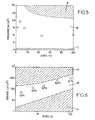
- the figure 7 represents a pulse at maximum power, controlled for 3 seconds. However, there are rising and falling fronts of the light output delivered as a function of time, due to the inertia of the lamps. Nevertheless, referring now to the figure 5 however, such an impulse allowed to anneal a thin layer of CIS by crystallizing it satisfactorily so as to obtain good photovoltaic properties.
- the annealing operating range (zone B) in terms of " power / duration " torque is delimited by a crystallization curve (lower power zone) and a degradation curve of the film (upper power zone).
- the Applicants have sometimes found a degradation of the films, in particular the underlying molybdenum layer.
- crystallization is insufficient and evaporation of selenium may simply occur, the saturation vapor pressure of selenium being already significant at 200 ° C.
- An experimental point of the figure 5 (apart from the first mentioned point) can correspond to one or more successive light pulses, separated by periods without illumination.
- a more accurate representation of these experimental points appears on the figure 6 , showing " energy supplied / duration " pairs, at logarithmic scales on the abscissa and on the ordinate. The domains are delimited by substantially linear curves with such scales.
- the Applicants have found that for a layer thickness close to one micrometer deposited on a glass substrate, the power transferred to the layer had to be greater than a few watts per cm 2 to begin a satisfactory crystallization.
- Advantageous annealing is obtained for a power greater than 15 W / cm 2 , for a duration of less than a few tens of seconds.
- the thin layer CM after annealing, is advantageously recrystallized in a substantially equivalent manner, or even better, than what is obtained after conventional annealing, under the pressure of selenium vapor, at temperatures above 450.degree. for periods of about one hour.
- the premixed structure of the electrodeposited precursor is likely to promote the recrystallization process, however with much lower durations than conventional annealing.
- the premixed structure obtained after the electroplating step allows a faster and more controllable crystallization, compared to the process described above thin film sputtering deposition according to the structure called " in sheets ".
- the electrolyzed precursor matrix obtained after the deposition step comprises constituents intimately mixed on the atomic scale, these constituents do not need to diffuse over long lengths (with respect to inter-atomic distances) to form the CuInSe phase 2 during annealing.
- the relatively short annealing time limits the risk of deformation of the substrate S due to too high temperatures.
- This substrate may be glass but also in any other material with lower temperature increases.
- the combination of a solution deposit (by electrochemistry or by precipitation), at room temperature, and rapid annealing allows recrystallization of the films without the substrate having time to be altered in a manner detrimental to the intended application.
- deposits on deformable substrates for example plastic
- a deposit on polymer substrate such as KAPTON ® may be annealed from one or more pulses of a neighboring illumination power of 25 W / cm 2 and a few seconds.
- Electrochemical deposition on a conductive metal substrate advantageously makes it possible to overcome the underlying molybdenum layer.
- the deposition on a flexible substrate advantageously makes it possible to produce materials for photovoltaic applications that can be embedded in space aircraft, because of their light weight and their folding capacity.
- the figure 8 represents an X-ray diffraction pattern of a CIS film before and after fast annealing (full-line and dotted line curves, respectively).
- the line in the plane (112) characteristic of the CIS, is very broad and not very intense, which shows that the electrodeposited precursor is poorly crystallized.
- the ternary phase of CIS appears here mainly, whereas the phases of binaries or the elementary phases (for example Cu) hardly appear.
- the line (112) is thinner and more intense.
- photovoltaic cells are produced by depositing a thin layer of CdS and then a layer of ZnO by sputtering ( figure 4 ). If necessary, it can be provided a last layer or an antireflection stack AR, so as to increase the efficiency of the solar cell.
- the cells thus produced have photovoltaic properties leading to yields of the order of 8% ( figure 6 ), without gallium and without the anti-reflection layer AR represented on the figure 4 .
- the combination of electrochemical deposition, pre-mixed precursor elements and rapid annealing of the precursor layer is a faster, cheaper process (since the salts present in bath B can be used in a subsequent electrolysis) and non-polluting (thus avoiding the toxic emissions of H 2 Se).
- the deposition step takes place at ambient temperature and pressure (approximately 20 ° C. and 1 atm, respectively). As indicated with reference to the table above, this process offers the possibility of treating large areas, with good uniformity.
Landscapes
- Photovoltaic Devices (AREA)
- Electroplating Methods And Accessories (AREA)
Description
- La présente invention concerne le domaine des dépôts de couches minces de semi-conducteurs pour des applications photovoltaïques.
- Des couches minces de diséléniure et/ou disulfure de cuivre et d'indium et/ou de gallium (CIGS) sont déposées sur substrat pour fabriquer des cellules photovoltaïques. De tels composés, de formule générale CuGaxIn1-xSe2-ySy (avec x compris entre 0 et 1 et y compris entre 0 et 2), sont considérés comme très prometteurs et pourraient constituer la prochaine génération de cellules solaires en couches minces. Les matériaux semi-conducteurs CIGS ont une largeur de bande interdite ("gap" direct) compris entre 1,0 et 1,6 eV qui permet une forte absorption des radiations scolaires dans le visible. Des rendements de conversion records, supérieurs à. 18%, ont été obtenus récemment sur des cellules de petites surfaces.
- Les composés CIGS sont aussi dénommés I-III-VI2, en référence à la nature chimique de leurs constituants, où :
- l'élément Cu représente un élément de la colonne I (colonne 1B de la table de classification de Mendeleïev),
- l'élément In et/ou l'élément Ga représentent des éléments de la colonne III (colonne 3B de la table de classification de Mendeleiev), et
- l'élément Se et/ou l'élément S représentent un élément de la colonne VI (colonne 6B de la table de classification de Mendeleïev).
- On compte donc approximativement deux atomes de la colonne VI pour un atome de la colonne I et un atome de la colonne III, dans le domaine 'monophasé autour de la composition I-III-VI2 du CIGS.
- Les couches de CIGS utilisées pour la conversion photovoltaïque doivent présenter un caractère semi-conducteur de type p et de bonnes propriétés de transport de charge. Ces propriétés de transport de charge sont favorisées par une bonne cristallinité. Ainsi, les composés CIGS doivent être au moins partiellement cristallisés pour posséder des propriétés photovoltaïques suffisantes pour leur application à la fabrication de cellules solaires. Les composés CIGS cristallisés ont une structure cristallographique correspondant au système des chalcopyrites ou des sphalérites, suivant la température de dépôt.
- Les couches minces de CIGS, lorsqu'elles sont déposées à basse température (dépôt de précurseur), sont faiblement cristallisées, voire amorphes, et un recuit des couches par apport thermique doit être réalisé pour obtenir une amélioration de la cristallisation du CIGS et des propriétés de transport de charge satisfaisantes.
- Néanmoins, aux températures permettant une cristallisation au moins partielle du CIGS, l'un des éléments constitutifs du CIGS (en principe le sélénium Se) est plus volatil que les autres éléments. Il est donc difficile d'obtenir du CIGS cristallisé avec la composition souhaitée (proche de la stoechiométrie I-III-VI2) sans rajouter du sélénium pour le recuit de la couche de précurseur.
- De plus, pour obtenir un caractère semi-conducteur de type p (conduction par trous), la composition des couches doit présenter un léger écart à la stoechiométrie I-III-VI2, en faveur de l'élément VI.
- C'est ainsi que dans la fabrication de couches minces de CIGS pour des applications photovoltaïques, 'les réalisations de l'art antérieur utilisent un recuit des dépôts précurseurs en présence d'un excès de sélénium en phase vapeur.
- Les meilleurs rendements de conversion photovoltaïque à partir de CIGS (supérieurs à 17%) ont été obtenus en préparant des couches minces par évaporation. Cependant, l'évaporation est une technique coûteuse et difficile à mettre en oeuvre à l'échelle industrielle notamment en raison de problèmes de non-uniformité des dépôts de couches minces sur de grandes surfaces et d'un faible rendement de l'utilisation des matières premières.
- La pulvérisation cathodique (ou "sputtering") est mieux adaptée aux grandes surfaces mais elle nécessite des équipements de vide et des cibles de précurseurs très coûteux. On entend par "précurseurs" des composés intermédiaires dont les propriétés physico-chimiques sont distinctes de celles de CIS (ou de CIGS) et les rendent inaptes à la conversion photovoltaïques. Ils sont déposés initialement sous forme de couche mince, cette couche mince étant ensuite traitée pour former le dépôt souhaité de CIGS.
- Le dépôt par électrochimie offre une alternative avantageuse. Cependant, les difficultés rencontrées portent sur le contrôle de la qualité des précurseurs électrodéposés (composition, morphologie) et leur traitement en vue de conférer des propriétés électroniques adéquates pour la conversion photovoltaïque. Plusieurs approches ont été proposées pour surmonter ces difficultés parmi lesquelles :
- l'électrodéposition séparée, ou séquentielle, des précurseurs Cu puis In, suivie d'un ajout de Se (étape dite de "sélénisation"), telle que décrite dans
US-4 581 108 ; - l'électrodéposition de binaires (Cu, In), en présence d'une suspension de Se, telle que décrite dans
US-5 275 714 . - Il est en effet plus facile d'apporter un seul précurseur à la fois.
- Des développements plus récents (
US-5 730 852 ,US-5 804 054 ) proposent une électrodéposition qui revient à déposer une couche de précurseurs de composition CuxInyGazSen (avec x, y et z compris entre 0 et 2, et n compris entre 0 et 3), en utilisant une méthode par courants pulsés. L'électrodéposition est suivie d'une étape d'évaporation des éléments In, Ga et Se, afin d'accroître leur teneur par rapport à la couche électrolysée. - En ce qui concerne l'électrodéposition "pure", c'est-à-dire sans étape d'évaporation et à la stoechiométrie I-III-VI2, les meilleurs rendements sont de 6 à 7% environ, comme l'indiquent les publications :
- GUILLEMOLES et al., Advanced Materials, 6 (1994) 379 ;
- GUILLEMOLES et al., J. Appl. Phys., 79 (1996) 7293.
- Ces publications indiquent en outre que de meilleurs résultats sont obtenus lorsque des recuits sont effectués sous pression de vapeur de sélénium, à des températures supérieures à 450°C, sous vide. On applique alors un recuit conventionnel dans un four à diffusion, sous pression de Se élémentaire. Toutefois, de tels recuits sont relativement longs (de l'ordre d'une à quelques heures).
- Le document
DE 19917758 A1 décrit la fabrication d'une couche CIS à partir d'un dépôt ternaire par électrochimie. L'approvisionnement de sélénium dans le four à recuit est évité par un recuit à échauffement très rapide. - Le document
US-5 578 503 décrit un procédé en deux étapes, qui prévoit d'abord un dépôt par pulvérisation cathodique (ou "sputtering"), puis un recuit rapide (à lampes) des précurseurs ainsi déposés. En particulier, des éléments précurseurs Cu, In et Se sont déposés séparément sous forme élémentaire (Cu(0), In(0) et Se(0)) ou sous forme de binaires (tels que In2Se3). Ainsi, la structure initialement déposée avant recuit est essentiellement hétérogène et se présente sous la forme d'une multiplicité de feuillets successifs (empilements de Cu0/In0/Se0 ou Cu0/In2Se3, ou encore une combinaison des deux) dans le sens de l'épaisseur de la couche. Ce mélange de précurseurs subit ensuite un recuit rapide, comprenant une montée en température suivie d'un pallier nécessaire pour homogénéiser la couche de CIS. Néanmoins, la couche mince déposée par pulvérisation et de structure hétérogène en feuillets supporte mal, notamment mécaniquement, des montées brusques eh température. Le coefficient de dilatation en température de la couche étant spatialement inhomogène, des problèmes de décollement de cette couche peuvent apparaître durant l'étape de recuit. Un tel procédé, bien qu'avantageux, n'est donc pas encore complètement satisfaisant. - Plus généralement, les procédés de dépôt par évaporation ou par pulvérisation (sputtering) utilisent des sources qui sont couramment constituées d'éléments purs, ou le cas échéant de binaires, mais rarement de ternaires. Une difficulté survient dans la mise en oeuvre de tels procédés. Elle consiste dans le transfert des éléments de la source vers le substrat. Ce transfert n'est pas le même pour tous les éléments et la vitesse d'évaporation ou le taux de pulvérisation peuvent être différents pour un élément par rapport à l'autre. En particulier, à haute température, les tensions de vapeur des éléments (leur volatilité) peuvent être très différentes. Cet effet est d'autant plus pénalisant que le nombre des éléments dans l'alliage à obtenir est grand
- La présente invention vient améliorer la situation.
- Elle propose à cet effet un procédé de fabrication en couches minces d'alliages semi-conducteurs I-III-VI2, pour des applications photovoltaïques, selon la revendication 1.
- On entend par "grains nanométriques", des grains d'alliages qui, avantageusement, présentent majoritairement une nature physico-chimique proche de celle de l'alliage visé à l'étape b) (aussi bien en termes de composition que de liaisons entre atomes, notamment) et pouvant atteindre jusqu'à quelques dizaines de nanomètres.
- L'ensemble des grains forme alors une matrice avantageusement compacte et capable de supporter une augmentation brusque en température pendant l'étape de recuit b).
- Ainsi, la présente invention se manifeste globalement par l'association de deux étapes consistant en :
- la préparation d'un précurseur dont les éléments sont intimement liés, ce précurseur étant de morphologie capable de supporter le recuit rapide de l'étape b), et
- le recuit rapide de ce précurseur, tel que la cinétique du traitement soit suffisamment rapide pour limiter l'exodiffusion de l'élément VI (du fait de sa volatilité) pendant le recuit, tout en permettant une cristallisation satisfaisante de la couche.
- De plus, comme indiqué ci-avant, la conservation de l'élément VI dans la couche après recuit confère un caractère semi-conducteur de type p, favorable à la conversion photovoltaïque.
- Selon l'invention, tant pour une rapidité que pour une simplicité de mise en oeuvre industrielle, ladite couche mince est déposée à l'étape a) par électrochimie.
- Dans une réalisation préférée, le recuit de l'étape b) s'effectue par éclairement, de préférence direct, à partir d'une source de lumière. En variante, le recuit s'effectue par induction.
- Pour un recuit de CIS (ou CIGS) à l'étape b), la température de la couche est préférentiellement élevée à plus de 450°C.
- Avantageusement, le recuit rapide de l'étape b) peut s'effectuer en transférant à la couche mince une densité de puissance d'éclairement de l'ordre de la dizaine de Watts par cm2 et pendant des durées inférieures ou de l'ordre de la dizaine de secondes.
- Le rendement photovoltaïque des couches minces obtenues après recuit peut être de l'ordre ou même supérieur à 8%, dans ces conditions.
- D'autres caractéristiques et avantages de la présente invention apparaîtront à la lecture de la description détaillée ci-après et à l'examen des dessins annexés, sur lesquels :
- la
figure 1 représente schématiquement une installation de dépôt, par électrochimie, d'une couche mince de CIS ; - la
figure 2 représente schématiquement l'aspect de la structure sous forme de matrice d'un précurseur avant recuit, à l'échelle nanométrique ; - la
figure 3 représente une installation de recuit rapide, par éclairage de la couche mince obtenue par électrodéposition ; - la
figure 4 représente schématiquement la structure, en couches minces, d'une cellule destinée à des applications photovoltaïques ; - la
figure 5 illustre, à titre d'exemple pour du CIS, des couples de durées (abscisses) et de densités moyennes de puissance d'éclairement (ordonnées) permettant de cristalliser au moins partiellement une couche sans la dégrader ; - la
figure 6 illustre, selon une autre représentation (ici en échelles logarithmiques), des couples de durées (abscisses) et d'énergies fournies à la couche (ordonnées) permettant de cristalliser au moins partiellement une couche de CIS sans la dégrader et d'obtenir les rendements photovoltaïques indiqués en-dessous des points expérimentaux à titre illustratif ; - la
figure 7 illustre à titre d'exemple un profil temporel d'une densité de puissance transférée à la couche, pendant une impulsion lumineuse ; - la
figure 8 illustre des pics d'intensité de rayons X obtenus pour des orientations θ variables dans l'analyse d'une couche de CIS électrodéposée (courbe en traits pleins) et traitée par recuit rapide (courbe en traits pointillées). - En se référant à la
figure 1 , des couches minces (ou "films") de diséléniure de cuivre et d'indium sont obtenues à pression et température ambiante par électrodéposition d'un film précurseur CM sur un substrat de verre S, recouvert de molybdène Mo au préalable (figure 4 ). Avantageusement, le substrat S est initialement recouvert d'une couche supplémentaire, conductrice, électronique, par exemple métallique ou sous forme d'oxyde (non représentée). Cette couche conductrice peut en outre reposer sur une ou plusieurs sous-couches servant à une application spécifique (barrière de diffusion, miroir ou autre) dans la fabrication de cellules photovoltaïques. - En se référant à la
figure 1 , l'électrodéposition est effectuée dans un bain B contenant un sel d'indium, un sel de cuivre et de l'oxyde de sélénium dissout. - Les sels sont mélangés pendant le dépôt grâce à un agitateur tournant M immergé dans le bac d'électrochimie B.
- Ainsi, la couche mince est obtenue par électrodéposition d'un précurseur dont les éléments constitutifs sont intimement pré-mélangés.
- Selon des exemples plus générales que l'invention revendiquée, les paramètres du dépôt peuvent être choisis dans des plages suivantes :
- Les concentrations des éléments du précurseur (sous forme de sels et d'oxyde dans la solution) sont comprises entre 10-4 et 10-1 mol/l. Préférentiellement, le pH de la solution est fixé entre 1 et 3. Le potentiel appliqué à l'électrode de molybdène (cathode Ca) est compris entre -0,8 volt et -1,9 volt par rapport à l'électrode de référence REF, ici au sulfate mercureux.
- Des dépôts de couches minces d'épaisseur comprise entre 0,1 et 3 µm sont obtenus, avec des densités de courant d'environ 0,5 à 4 mA/cm2.
- Selon l'invention, un dépôt de précurseur est réalisé à partir d'un bain dont les concentrations sont les suivantes : [Cu(SO4)]= 1,0.10-3 mol/l, [In2(SO4)3]= 6,0.10-3 mol/l, [H2SeO3]= 1,7.10-3 mol/l, [Na2(SO4)]= 0,1 mol/l.
- Le pH du bain est de 2. Les précurseurs sont déposés par réaction cathodique à potentiel imposé, de -1 volt par rapport à l'électrode de référence au sulfate mercureux. La densité de courant est de -1 mA/cm2.
- Dans la mesure où les sels de cuivre et d'indium, ainsi que l'oxyde de sélénium dissout, sont mélangés dans la solution du bain B, à la fin de l'étape a) précitée d'électrodéposition, on obtient un précurseur dont les éléments sont intimement pré-mélangés.
- Le film de précurseur obtenu est dense, adhérent, de morphologie homogène et sa composition est proche de la composition stoechiométrique Cu (25%), In (25%), Se (50%).
- Le tableau ci-après indique la composition atomique en pourcentage, en différents points (points 1 à 5) d'un film de précurseur CIS électrodéposé sur un substrat d'environ 10 cm2, ces compositions ayant été analysées par microsonde électronique (WDX).
Cu (% atom.) In (% atom.) Se (% atom.) In/Cu Se/(In+Cu) Point 1 22.5 24,3 53,3 1,080 1.14 Point 2 22,7 24,4 52.9 1,075 1,12 Point 3 22.6 24,6 52,8 1,088 1.12 Point 4 22,9 24,5 52,6 1,070 1,11 Point 5 22.9 24.3 52.8 1.061 1,12 Moyenne 22,72 24,42 52,88 1,075 1,122 Ecart-type 0,179 0,130 0,259 0,010 0,011 - En se référant à la colonne relative à la composition en sélénium Se, on constate néanmoins un léger excès en sélénium par rapport à la quantité nécessaire pour s'associer au cuivre sous forme de Cu2Se et à l'indium sous forme de In2Se3. Dans l'exemple décrit, cet excès de sélénium est d'environ 10%.
- L'excès en sélénium est un élément favorable à l'obtention d'un caractère semi-conducteur de type p de la couche après l'étape de recuit, permettant une conversion photovoltaïque satisfaisante.
- De même, on constate un léger excès en indium, par rapport au cuivre, d'environ 7%. Cet excès d'indium est apparu aussi comme jouant un rôle favorable pour l'obtention des propriétés photovoltaïques.
- On peut vérifier que le dépôt respecte une uniformité satisfaisante en composition dans le plan de la couche mince. De plus, les Demandeurs ont constaté que cette uniformité était aussi respectée en épaisseur de couche, notamment en procédant à des analyses fines de type SIMS ("Secondary Ion Mass Spectroscopy") ou EELS ("Electron Energy Loss Spectroscopy").
- Toutefois, il est aussi possible de créer un gradient de composition dans la couche déposée, par exemple en faisant varier la proportion de composition en cuivre en fonction de l'épaisseur (notamment en jouant sur la valeur du potentiel électrochimique imposé pendant l'électrodéposition). Un tel gradient de composition permet avantageusement d'obtenir un confinement des porteurs dans les applications photovoltaïques visées.
- De telles analyses fines (SIMS, EELS) on montré en outre que la composition du précurseur électrodéposé est majoritairement voisine de celle désirée pour l'alliage final, dans des grains GR de quelques dizaines de nanomètres, représentés à titre illustratif sur la
figure 2 . Dans la composition finale de l'alliage obtenu après l'étape de recuit rapide, l'excédent en sélénium est bien inférieur à l'ordre de 1%, mais est suffisant pour "doper" (comme un dopage de type p à environ 1016 cm-3) le CIS recuit. On comprendra donc que la composition de l'alliage obtenu après recuit est très proche de celle de l'alliage stoechiométrique I-III-VI2. C'est sensiblement cette composition qui est essentiellement présente dans les grains GR du précurseur électrodéposé, avant recuit. - En se référant à la
figure 2 , les films obtenus après l'étape d'électrodéposition sont constitués d'une matrice globalement amorphe (ou peu cristallisée par rapport à l'alliage après recuit) mais comprenant majoritairement des grains GR de CIS (cristallites de l'ordre de quelques dizaines de nanomètres). - On entend par le terme "matrice" une nature composite de la couche susceptible de présenter plusieurs phases possibles : ternaire (dans le cas du CIS), binaire (par exemple CuxSe avec x voisin de 2 et InxSey avec x voisin de 2 et y voisin de 3), ou même élémentaire (sélénium ou autre). Comme indiqué ci-avant, les grains GR sont de composition proche de celle désirée pour l'alliage final, par exemple CuInSe2 dans le cas du CIS, alors que globalement le précurseur présente un excès de sélénium d'environ 10%. On constate ainsi qu'en dehors des grains ou à la superficie des grains tels que représentés sur la
figure 2 à titre d'exemple, des phases PH plus riches en sélénium sont présentes, par exemple du sélénium élémentaire Se ou du binaire CuSe. - Le volume de la couche occupé par les grains GR est néanmoins largement prépondérant par rapport à celui occupé par ces phases PH. Le précurseur ainsi électrodéposé présente globalement une nature physico-chimique majoritairement proche de celle de l'alliage final désiré, et ce, non seulement en terme de composition mais aussi en terme de liaisons chimiques, qui sont celles de l'alliage désiré dans les grains GR. Ainsi, le mélange intime des éléments (donc les faibles distances de migration des éléments durant le recuit) contribue à ce que l'alliage ne se dégrade pas pendant le recuit.
- Outre les grains majoritaires de CIS, des grains de binaires de compositions voisines de Cu2Se et In2Se3 (non représentés sur la
figure 2 ) peuvent aussi coexister localement. Ces grains, pendant l'étape b) de recuit rapide, sont capables aussi de réagir ensemble pour donner un plus gros grain cristallisé de composition proche de CuInSe2. - Même si les risques d'exodiffusion pendant le recuit rapide sont limités, on dépose en outre, avant l'étape de recuit, une couche recouvrant la couche de précurseur pour limiter encore une exodiffusion d'éléments du précurseur, tels que Se, pendant l'étape de recuit.
- Le bon degré d'oxydation des éléments ainsi mélangés pendant l'étape d'électrodépôt évite des réactions chimiques incontrôlées pendant le recuit. En d'autres termes, l'énergie libre de réaction est relativement faible, ce qui évite l'apparition de réactions fortement exothermique, comme celles de l'indium et du sélénium élémentaires dans le CIS. En effet, les éléments In et Se sous forme élémentaire In0, Se0 sont très réactifs. Dans un procédé de dépôt dit "en feuillets" tel que décrit ci-avant, un recuit trop rapide pourrait mener à une dégradation de la couche, notamment pour cette raison.
- En outre, cette matrice est sensiblement homogène dans la répartition spatiale de son coefficient de dilatation. Elle est donc capable de supporter une augmentation brusque en température pendant l'étape de recuit par éclairement, en comparaison de la structure hétérogène, en feuillets, précitée.
- De façon plus générale, la nature physico-chimique (degré d'oxydation, densité, coefficient de dilatation en température) du précurseur est majoritairement très proche de la phase cristallisée CuInSe2, ce qui limite fortement la création d'inhomogénéités pendant le recuit (gonflements, décollements localisés). Ainsi, on comprendra que la matrice obtenue après l'étape d'électrodéposition et comprenant les éléments du précurseur pré-mélangés permet avantageusement d'effectuer un recuit rapide, cette matrice étant capable de supporter des puissances transférées supérieures ou égales à 10W/cm2.
- Les films de précurseur après l'étape de dépôt ne possèdent que de faibles propriétés photovoltaïques en l'état. En fait, ces propriétés photovoltaïques sont obtenues seulement après un traitement par recuit thermique. La recristallisation de la couche mince permet d'obtenir de bonnes propriétés de transfert de charge pour la conversion photovoltaïque.
- Selon l'une des caractéristiques de l'invention, ce traitement thermique est effectué à partir d'un recuit rapide de la couche mince CM électrodéposée. En se référant à la
figure 3 , la couche mince CM électrodéposée sur le substrat S est disposée sur un porte-échantillon PE qui est, de préférence, capable de se déplacer dans un plan horizontal (déplacement le long de l'axe X, tel que représenté sur lafigure 3 ), relativement à une source de lumière LA qui, dans l'exemple décrit, est une rampe de lampes halogènes à forte puissance de rayonnement, avantageusement dans une bande d'absorption optique de la couche mince CM. Ainsi, on entend, dans l'exemple décrit, par "recuit rapide" un éclairement du film CM de manière à permettre une cristallisation au moins partielle de cette couche mince, pendant des durées totales de l'ordre de la dizaine de secondes. Ce recuit rapide est effectué dans un four à lampe (figure 3 ) dans lequel la couche mince peut recevoir par incidence directe des puissances rayonnées de l'ordre de 10W/cm2 et plus. En variante, on peut prévoir un recuit rapide par chauffage à induction à partir d'une boucle de courant. - L'énergie transférée à la couche mince pendant le recuit rapide rend le sélénium actif (le sélénium étant en particulier excédentaire à l'extérieur des grains GR), ce qui amorce une agglomération des grains GR comme par frittage. Les grains GR, nanométriques dans le précurseur, se joignent en formant de plus gros grains, de taille sensiblement micrométrique. Le sélénium en excès joue, pendant le recuit rapide, un rôle important d'agent de recristallisation et de passivation des défauts. Ce rôle est favorisé notamment par les faibles distances interatomiques qu'a le sélénium à parcourir. La structure en matrice homogène du précurseur joue quant à elle, pendant le recuit, un rôle de "couvercle interne" pour le sélénium (par confinement) en limitant fortement son exodiffusion.
- Avantageusement, les recuits peuvent être effectués sous pression atmosphérique, à l'air ambiant, ou encore sous pression de gaz neutre (par exemple argon ou azote).
- Dans l'exemple décrit, la puissance maximale par unité de surface que reçoit effectivement la couche mince est estimée à 25 W/cm2, en tenant compte de la puissance nominale des lampes, de la dispersion de la lumière entre les lampes et la couche mince, des pertes par réflexion, et autres.
- La
figure 7 représente une impulsion à une puissance maximale, commandée pour 3 secondes. On constate cependant des fronts de montée et de descente de la puissance lumineuse délivrée en fonction du temps, dus à l'inertie des lampes. Néanmoins, en se référant maintenant à lafigure 5 , une telle impulsion a permis toutefois de recuire une couche mince de CIS en la cristallisant de façon satisfaisante de manière à obtenir de bonnes propriétés photovoltaïques. - La
figure 5 représente des points expérimentaux (carrés foncés) correspondant à des couples puissance lumineuse moyenne/durée de recuit qui ont permis d'obtenir des couches cristallisées. L'impulsion précitée de 3 secondes correspond au premier point à gauche du graphique. Les zones A, B et C, délimitées par des courbes en traits pointillés, correspondent respectivement à : - des couples puissance/durée pour lesquels la puissance est trop importante (zone A) et la couche est susceptible d'être dégradée pendant le recuit,
- des couples puissance/durée permettant d'obtenir une cristallisation satisfaisante de la couche (zone B), et
- des couples puissance/durée pour lesquels la puissance n'est pas suffisante pour recuire correctement la couche (zone C).
- Ainsi, le domaine d'exploitation du recuit (zone B) en termes de couple "puissance/durée" est délimité par une courbe de cristallisation (zone inférieure en puissance) et une courbe de dégradation du film (zone supérieure en puissance). A fortes puissances, les Demandeurs ont constaté parfois une dégradation des films, notamment de la couche de molybdène sous-jacente. A des puissances trop faibles et/ou des temps trop longs, la cristallisation est insuffisante et une évaporation du sélénium risque simplement de se produire, la tension de vapeur saturante du sélénium étant déjà significative à 200°C.
- Un point expérimental de la
figure 5 (hormis le premier point précité) peut correspondre à une ou plusieurs impulsions lumineuses successives, séparées par des périodes sans éclairement. Une représentation plus exactes de ces points expérimentaux apparaît sur lafigure 6 , montrant des couples "énergie fournie/durée", à des échelles logarithmiques en abscisses et en ordonnées. Les domaines sont délimités par des courbes sensiblement linéaires avec de telles échelles. - Bien entendu, ces domaines sont représentés sur les
figures 5 et 6 à titre d'illustration : ils ne servent qu'à la compréhension des phénomènes en jeu. - Néanmoins, les Demandeurs ont constaté que, pour une épaisseur de couche voisine du micromètre déposée sur un substrat en verre, la puissance transférée à la couche devait être supérieure à quelques Watts par cm2 pour commencer une cristallisation satisfaisante. Un recuit avantageux est obtenu pour une puissance supérieure à 15 W/cm2, pendant une durée inférieure à quelques dizaines de secondes.
- La couche mince CM, après recuit, est avantageusement recristallisée de façon sensiblement équivalente, voire meilleure, par rapport à ce qui est obtenu à l'issue des recuits classiques, sous pression de vapeur de sélénium, à des températures supérieures à 450° C et pendant des durées voisines d'une heure.
- Ainsi, selon l'un des avantages que procure la présente invention, la structure pré-mélangée du précurseur électrodéposé est de nature à favoriser le processus de recristallisation, cependant avec des durées bien inférieures à celles des recuits classiques.
- En particulier, la structure pré-mélangée obtenue après l'étape d'électrodéposition permet une cristallisation plus rapide et plus contrôlable, par rapport au procédé décrit ci-avant de dépôt par pulvérisation de couches minces selon la structure dite "en feuillets". En effet, la matrice de précurseurs électrolysée obtenue après l'étape de dépôt comprend des constituants intimement mélangés à l'échelle atomique, ces constituants n'ayant pas besoin de diffuser sur de grandes longueurs (par rapport aux distances inter-atomiques) pour former la phase CuInSe2 pendant le recuit.
- Par ailleurs, dans les procédés classiques, la quantité de sélénium en excès est habituellement beaucoup plus importante que 10% après l'étape de dépôt et avant le recuit, ce qui grève le coût d'obtention de bons matériaux photovoltaïques. Comme indiqué ci-avant, une autre solution de l'état de la technique consiste en une sélénisation en présence du gaz H2Se. Cependant, ce gaz est très réactif et très toxique. Ainsi, avec le procédé objet de la présente invention, on obtient des performances photovoltaïques avec, néanmoins, des quantités initiales relativement faibles de sélénium directement après le dépôt par électrochimie et sans ajout de sélénium pendant le recuit. En effet, les cinétiques rapides pendant le recuit limitent fortement l'exodiffusion de l'élément Se hors de la couche. Cet effet permet avantageusement de s'affranchir de l'utilisation habituelle qui est faite du gaz toxique H2Se dans les procédés de sélénisation, ainsi que de tout autre apport de Se pendant l'étape de recuit.
- Toutefois, l'utilisation d'un recuit rapide au sens de la présente invention est également compatible avec l'apport d'éléments VI (par exemple de sélénium ou de soufre pour augmenter la largeur de bande interdite du semi-conducteur), pendant la phase de cristallisation.
- Selon un autre avantage que procure la présente invention, le temps relativement court de recuit permet de limiter les risques de déformation du substrat S due à des températures trop élevées. Ce substrat peut être en verre mais aussi dans tout autre matériau supportant de moindres élévations en température. En effet, la combinaison d'un dépôt en solution (par électrochimie ou par précipitation), à température ambiante, et d'un recuit rapide permet une recristallisation des films sans que le substrat ait le temps d'être altéré de manière préjudiciable à l'application visée. Ainsi, des dépôts sur substrats déformables (par exemple en matière plastique) peuvent être prévus. Avantageusement, un dépôt sur substrat en polymère tel que du KAPTON® peut être recuit à partir d'une ou de plusieurs impulsions d'une puissance d'éclairement voisine de 25 W/cm2 et de quelques secondes. En outre, des résultats satisfaisants ont été aussi obtenus pour du CIS électrodéposé sur un substrat métallique, tel qu'une feuille d'aluminium. Les Demandeurs ont alors constaté que le substrat métallique supporte avantageusement le recuit rapide permettant une recristallisation satisfaisante du CIS. Un dépôt par électrochimie sur un substrat métallique, conducteur, permet avantageusement de s'affranchir de la couche de molybdène sous-jacente. Par ailleurs, le dépôt sur un substrat souple (tel qu'une feuille d'aluminium ou un panneau de KAPTON) permet avantageusement de produire des matériels pour des applications photovoltaïques qui peuvent être embarqués dans des aéronefs spatiaux, en raison de leur légèreté et de leur capacité de pliage.
- La
figure 8 représente un diagramme de diffraction des rayons X d'un film de CIS avant et après recuit rapide (respectivement courbe en trait plein et en traits pointillés). Avant recuit, la raie selon le plan (112), caractéristique du CIS, est très large et peu intense, ce qui montre que le précurseur électrodéposé est mal cristallisé. Néanmoins, la phase ternaire du CIS apparaît ici majoritairement, alors que les phases de binaires ou les phases élémentaires (par exemple Cu) n'apparaissent pratiquement pas. On remarque ainsi essentiellement une superposition des raies de diffraction selon le plan (112) du CIS avant et après recuit. Cependant, après recuit, la raie (112) est plus fine et intense. - Après recuit rapide de la couche CM, des cellules photovoltaïques sont réalisées en déposant une fine couche de CdS puis d'une couche de ZnO par pulvérisation cathodique (
figure 4 ). Le cas échéant, il peut être prévu une dernière couche ou un empilement anti-reflet AR, de manière augmenter le rendement de la cellule solaire. Les cellules ainsi réalisées présentent des propriétés photovoltaïques conduisant à des rendements de l'ordre de 8% (figure 6 ), sans gallium et sans la couche anti-reflet AR représentée sur lafigure 4 . - Ainsi, la combinaison d'un dépôt par électrochimie, d'éléments de précurseur pré-mélangés et d'un recuit rapide de la couche de précurseur constitue un procédé plus rapide, à moindre coût (puisque les sels présents dans le bain B peuvent être utilisés dans une électrolyse ultérieure) et non polluant (en s'affranchissant ainsi des émanations toxiques de H2Se). De plus, l'étape de dépôt a lieu à température et à pression ambiantes (respectivement 20° C environ et 1 atm). Comme indiqué en référence au tableau ci-avant, ce procédé offre la possibilité de traiter de grandes surfaces, avec une bonne uniformité.
Claims (8)
- Procédé de fabrication en couches minces d'alliages semi-conducteurs I-III-VI2, pour des applications photovoltaïques, dans lequel :a) on dépose par électrochimie, sur un substrat, une couche mince d'un précurseur de composition excédentaire en élément VI par rapport à la somme de la composition en élément I et en élément III, d'environ 10% par rapport à la composition d'alliage finale I-III-VI2, tout en mélangeant les éléments constitutifs du précurseur, l'élément I étant le cuivre, l'élément III étant l'indium et l'élément VI étant le sélénium, l'indium étant en excès, par rapport au cuivre, d'environ 7%, l'excès de sélénium étant d'environ 10%, le dépôt de précurseur étant réalisé à partir d'un bain dont les concentrations sont les suivantes : [Cu(SO4)] =1,0.10-3 mol/l, [In2(SO4)2]=6,0.10-3 mol/1, [H2SeO3]=1,7.10-3 mol/l, [Na2(SO4)]=0,1 mol/l, le ph du bain étant de 2, le précurseur étant déposé par réaction cathodique à potentiel imposé de -1 Volt par rapport à une électrode de référence au sulfate mercureux, et une densité de courant de -1 mA/cm2, de manière à conférer au précurseur une structure comportant des grains nanométriques d'alliages de composition I-III-VI2, joints par des phases plus riches en élément VI que la composition I-III-VI2, etb) on effectue, à partir d'une source de rayonnement électromagnétique, un recuit de la couche obtenue à l'étape a),
avec une puissance électromagnétique supérieure à 10 W/cm2, suffisante pour activer l'élément VI et faire réagir ensemble lesdits grains d'alliages, de manière à améliorer la cristallisation de ladite couche, et
pendant une durée inférieure à 30 secondes, suffisamment courte pour limiter l'exodiffusion de l'élément VI et obtenir sensiblement ladite composition I-III-VI2 dans la couche et conférer à ladite couche des propriétés photovoltaïques. - Procédé selon la revendication 1, dans lequel lesdits grains d'alliages sont de nature physico-chimique proche de celle de l'alliage obtenu à l'étape b), et forment ensemble une matrice capable de supporter une augmentation en température supérieure à 450°C pendant ladite durée de l'étape de recuit b).
- Procédé selon l'une des revendications précédentes, dans lequel la température de la couche est élevée à plus de 450°C à l'étape b).
- Procédé selon l'une des revendications précédentes, dans lequel la puissance transférée à la couche est de l'ordre de 20 W/cm2, pendant une durée inférieure à 10 secondes.
- Procédé selon l'une des revendications précédentes, dans lequel le substrat est réalisé dans une matière plastique.
- Procédé selon l'une des revendications précédentes, dans lequel le substrat est réalisé dans un matériau métallique, préférentiellement en aluminium.
- Procédé selon l'une des revendications précédentes, dans lequel on dépose en outre à l'étape a) une couche protectrice recouvrant la couche d'alliage et propre à limiter une exodiffusion d'élément VI hors de la couche d'alliage pendant l'étape de recuit b).
- Procédé selon la revendication 7, dans lequel ladite couche protectrice est soluble au moins après l'étape de recuit b).
Applications Claiming Priority (3)
| Application Number | Priority Date | Filing Date | Title |
|---|---|---|---|
| FR0205362 | 2002-04-29 | ||
| FR0205362A FR2839201B1 (fr) | 2002-04-29 | 2002-04-29 | Procede de fabrication de semi-conducteurs en couches minces a base de composes i-iii-vi2, pour applications photovoltaiques |
| PCT/FR2003/001282 WO2003094246A1 (fr) | 2002-04-29 | 2003-04-23 | Procede de fabrication de semi-conducteurs en couches minces a base de composes i-iii-vi2, pour applications photovoltaïques |
Publications (2)
| Publication Number | Publication Date |
|---|---|
| EP1500146A1 EP1500146A1 (fr) | 2005-01-26 |
| EP1500146B1 true EP1500146B1 (fr) | 2014-10-01 |
Family
ID=28800016
Family Applications (1)
| Application Number | Title | Priority Date | Filing Date |
|---|---|---|---|
| EP03747464.0A Expired - Lifetime EP1500146B1 (fr) | 2002-04-29 | 2003-04-23 | Procede de fabrication de semi-conducteurs en couches minces a base de composes i-iii-vi(2), pour applications photovoltaiques |
Country Status (8)
| Country | Link |
|---|---|
| US (1) | US7026258B2 (fr) |
| EP (1) | EP1500146B1 (fr) |
| JP (1) | JP4739750B2 (fr) |
| AU (1) | AU2003246852B2 (fr) |
| CA (1) | CA2483584C (fr) |
| ES (1) | ES2526694T3 (fr) |
| FR (1) | FR2839201B1 (fr) |
| WO (1) | WO2003094246A1 (fr) |
Families Citing this family (52)
| Publication number | Priority date | Publication date | Assignee | Title |
|---|---|---|---|---|
| EP1746662B1 (fr) * | 2004-05-11 | 2017-01-25 | Honda Motor Co., Ltd. | Procédé de fabrication d'une photopile en couche mince à base de chalcopyrite |
| US7732229B2 (en) * | 2004-09-18 | 2010-06-08 | Nanosolar, Inc. | Formation of solar cells with conductive barrier layers and foil substrates |
| SE527733C2 (sv) * | 2004-10-08 | 2006-05-23 | Midsummer Ab | Anordning och metod för att tillverka solceller |
| FR2886460B1 (fr) * | 2005-05-25 | 2007-08-24 | Electricite De France | Sulfurisation et selenisation de couches de cigs electrodepose par recuit thermique |
| DE102005062977B3 (de) * | 2005-12-28 | 2007-09-13 | Sulfurcell Solartechnik Gmbh | Verfahren und Vorrichtung zur Umsetzung metallischer Vorläuferschichten zu Chalkopyritschichten von CIGSS-solarzellen |
| US7507321B2 (en) * | 2006-01-06 | 2009-03-24 | Solopower, Inc. | Efficient gallium thin film electroplating methods and chemistries |
| DE102006004909A1 (de) * | 2006-02-01 | 2007-09-13 | Sulfurcell Solartechnik Gmbh | Verfahren zum Aufbringen von Alkaliionen auf die Oberfläche der CIGSSe-Absorberschicht einer Chalkopyrit-Solarzelle |
| US7736913B2 (en) * | 2006-04-04 | 2010-06-15 | Solopower, Inc. | Composition control for photovoltaic thin film manufacturing |
| US20070227633A1 (en) * | 2006-04-04 | 2007-10-04 | Basol Bulent M | Composition control for roll-to-roll processed photovoltaic films |
| US7892413B2 (en) * | 2006-09-27 | 2011-02-22 | Solopower, Inc. | Electroplating methods and chemistries for deposition of copper-indium-gallium containing thin films |
| US20100139557A1 (en) * | 2006-10-13 | 2010-06-10 | Solopower, Inc. | Reactor to form solar cell absorbers in roll-to-roll fashion |
| US20090183675A1 (en) * | 2006-10-13 | 2009-07-23 | Mustafa Pinarbasi | Reactor to form solar cell absorbers |
| US20080175993A1 (en) * | 2006-10-13 | 2008-07-24 | Jalal Ashjaee | Reel-to-reel reaction of a precursor film to form solar cell absorber |
| EP2179449A2 (fr) * | 2007-04-11 | 2010-04-28 | Craig Leidholm | Formation de couches d'absorbeurs photovoltaïques sur des substrats en forme de feuille |
| US7846750B2 (en) * | 2007-06-12 | 2010-12-07 | Guardian Industries Corp. | Textured rear electrode structure for use in photovoltaic device such as CIGS/CIS solar cell |
| US20080308147A1 (en) * | 2007-06-12 | 2008-12-18 | Yiwei Lu | Rear electrode structure for use in photovoltaic device such as CIGS/CIS photovoltaic device and method of making same |
| US7875945B2 (en) * | 2007-06-12 | 2011-01-25 | Guardian Industries Corp. | Rear electrode structure for use in photovoltaic device such as CIGS/CIS photovoltaic device and method of making same |
| US8425753B2 (en) * | 2008-05-19 | 2013-04-23 | Solopower, Inc. | Electroplating methods and chemistries for deposition of copper-indium-gallium containing thin films |
| US8409418B2 (en) * | 2009-02-06 | 2013-04-02 | Solopower, Inc. | Enhanced plating chemistries and methods for preparation of group IBIIIAVIA thin film solar cell absorbers |
| US7842534B2 (en) * | 2008-04-02 | 2010-11-30 | Sunlight Photonics Inc. | Method for forming a compound semi-conductor thin-film |
| US9646828B2 (en) * | 2008-04-02 | 2017-05-09 | Sunlight Photonics Inc. | Reacted particle deposition (RPD) method for forming a compound semi-conductor thin-film |
| EP2128903B1 (fr) | 2008-05-30 | 2017-02-22 | ATOTECH Deutschland GmbH | Additif d'électrodéposition pour le dépôt d'un metal ou d'un alliage binaire, ternaire, quaternaire ou pentanaire des éléments de groupe 11 (IB)-groupe 13 (lllA)-groupe 16 (VIA) |
| US20100098854A1 (en) * | 2008-10-17 | 2010-04-22 | Sunlight Photonics Inc. | Pressure controlled droplet spraying (pcds) method for forming particles of compound materials from melts |
| US8110428B2 (en) * | 2008-11-25 | 2012-02-07 | Sunlight Photonics Inc. | Thin-film photovoltaic devices |
| TWI421214B (zh) * | 2008-12-03 | 2014-01-01 | 財團法人工業技術研究院 | Ibiiiavia族非晶相化合物及應用於薄膜太陽能電池之ibiiiavia族非晶相前驅物的製造方法 |
| KR20110138259A (ko) * | 2009-03-25 | 2011-12-26 | 비코 인스트루먼츠 인코포레이티드 | 고증기압재료의 증착 |
| SG178227A1 (en) * | 2009-08-04 | 2012-03-29 | Precursor Energetics Inc | Polymeric precursors for cis and cigs photovoltaics |
| US8067262B2 (en) * | 2009-08-04 | 2011-11-29 | Precursor Energetics, Inc. | Polymeric precursors for CAIGS silver-containing photovoltaics |
| KR20120043050A (ko) * | 2009-08-04 | 2012-05-03 | 프리커서 에너제틱스, 인코퍼레이티드. | Caigas 알루미늄-함유 광기전체를 위한 중합체성 전구체 |
| CA2768612A1 (fr) * | 2009-08-04 | 2011-02-10 | Precursor Energetics, Inc. | Procedes pour absorbeurs photovoltaiques a stoichiometrie controlee |
| US7923628B2 (en) * | 2009-09-09 | 2011-04-12 | International Business Machines Corporation | Method of controlling the composition of a photovoltaic thin film |
| FR2951022B1 (fr) * | 2009-10-07 | 2012-07-27 | Nexcis | Fabrication de couches minces a proprietes photovoltaiques, a base d'un alliage de type i-iii-vi2, par electro-depots successifs et post-traitement thermique. |
| US7910396B2 (en) * | 2009-10-21 | 2011-03-22 | Sunlight Photonics, Inc. | Three-stage formation of thin-films for photovoltaic devices |
| US8012788B1 (en) | 2009-10-21 | 2011-09-06 | Sunlight Photonics Inc. | Multi-stage formation of thin-films for photovoltaic devices |
| WO2011084171A1 (fr) * | 2009-12-17 | 2011-07-14 | Precursor Energetics, Inc. | Précurseurs moléculaires pour l'optoélectronique |
| WO2012009212A2 (fr) * | 2010-07-12 | 2012-01-19 | Board Of Regents Of The University Of Texas System | Nanofils et procédés de fabrication et d'utilisation |
| KR20140007332A (ko) | 2010-09-15 | 2014-01-17 | 프리커서 에너제틱스, 인코퍼레이티드. | 박막 태양 전지 방법을 위한 알칼리 금속 함유 잉크 |
| US8563354B1 (en) | 2010-10-05 | 2013-10-22 | University Of South Florida | Advanced 2-step, solid source deposition approach to the manufacture of CIGS solar modules |
| FR2966282B1 (fr) * | 2010-10-18 | 2013-02-15 | Nexcis | Controle de la stoechiometrie de couches i-iii-vi pour des applications photovoltaiques a partir de conditions d'electrolyse perfectionnees. |
| US20130264526A1 (en) * | 2010-12-03 | 2013-10-10 | E I Du Pont De Nemours And Company | Molecular precursors and processes for preparing copper indium gallium sulfide/selenide coatings and films |
| US9157153B2 (en) * | 2012-02-21 | 2015-10-13 | Zetta Research and Development LLC—AQT Series | Closed-space annealing of chalcogenide thin-films with volatile species |
| US20140144507A1 (en) * | 2012-11-23 | 2014-05-29 | Samsung Sdi Co., Ltd. | Solar cell and method of manufacturing the same |
| US9276147B2 (en) | 2012-12-13 | 2016-03-01 | First Solar, Inc. | Methods of fabricating a photovoltaic module, and related system |
| DE102013209983A1 (de) | 2013-05-28 | 2014-12-18 | Zentrum für Sonnenenergie- und Wasserstoff-Forschung Baden-Württemberg | Verfahren zur Herstellung einer Dünnschichtsolarzelle und einer Verbindungshalbleiterschicht hierfür |
| JP6276610B2 (ja) * | 2014-02-28 | 2018-02-07 | 学校法人金沢工業大学 | 光電変換素子の製造方法およびp型半導体層の製造方法 |
| CN105633201B (zh) * | 2014-11-06 | 2017-06-16 | 中物院成都科学技术发展中心 | 钝化铜铟镓硒薄膜表面缺陷的电化学处理方法 |
| CN105633205B (zh) * | 2014-11-06 | 2017-03-29 | 中物院成都科学技术发展中心 | 修饰铜锌锡硫薄膜太阳电池吸收层表面性质的电化学处理方法 |
| CN105633204B (zh) * | 2014-11-06 | 2017-04-05 | 中物院成都科学技术发展中心 | 改善铜铟镓硒薄膜表面性质的电化学处理方法 |
| CN105633199B (zh) * | 2014-11-06 | 2017-04-05 | 中物院成都科学技术发展中心 | 改善铜锌锡硫薄膜表面性质的电化学处理方法 |
| CN105633200B (zh) * | 2014-11-06 | 2017-04-05 | 中物院成都科学技术发展中心 | 铜铟镓硒薄膜表面刻蚀的电化学处理方法 |
| CN105633203B (zh) * | 2014-11-06 | 2017-06-09 | 中物院成都科学技术发展中心 | 无水电化学刻蚀铜锌锡硫薄膜材料表面的方法 |
| CN121110152B (zh) * | 2025-11-12 | 2026-04-17 | 景德镇陶瓷大学 | 一种三元金属硫化物纳米晶薄膜及其制备方法和应用 |
Family Cites Families (5)
| Publication number | Priority date | Publication date | Assignee | Title |
|---|---|---|---|---|
| JPS63285974A (ja) * | 1987-05-18 | 1988-11-22 | Taizo Irie | CuInSe↓2薄膜の形成方法 |
| WO1994007269A1 (fr) * | 1992-09-22 | 1994-03-31 | Siemens Aktiengesellschaft | Procede rapide de realisation d'un semi-conducteur en chalcopyrite sur un substrat |
| JP2940782B2 (ja) * | 1993-12-27 | 1999-08-25 | 矢崎総業株式会社 | 太陽電池吸収層の製造方法 |
| US5674555A (en) * | 1995-11-30 | 1997-10-07 | University Of Delaware | Process for preparing group Ib-IIIa-VIa semiconducting films |
| DE19917758C2 (de) * | 1999-04-10 | 2003-08-28 | Cis Solartechnik Gmbh | Verfahren zur Herstellung einer CuInSe2(CIS)Solarzelle |
-
2002
- 2002-04-29 FR FR0205362A patent/FR2839201B1/fr not_active Expired - Lifetime
-
2003
- 2003-04-23 EP EP03747464.0A patent/EP1500146B1/fr not_active Expired - Lifetime
- 2003-04-23 US US10/512,961 patent/US7026258B2/en not_active Expired - Lifetime
- 2003-04-23 JP JP2004502366A patent/JP4739750B2/ja not_active Expired - Fee Related
- 2003-04-23 CA CA2483584A patent/CA2483584C/fr not_active Expired - Fee Related
- 2003-04-23 WO PCT/FR2003/001282 patent/WO2003094246A1/fr not_active Ceased
- 2003-04-23 AU AU2003246852A patent/AU2003246852B2/en not_active Ceased
- 2003-04-23 ES ES03747464.0T patent/ES2526694T3/es not_active Expired - Lifetime
Also Published As
| Publication number | Publication date |
|---|---|
| AU2003246852A1 (en) | 2003-11-17 |
| US20050215079A1 (en) | 2005-09-29 |
| JP2005524244A (ja) | 2005-08-11 |
| US7026258B2 (en) | 2006-04-11 |
| EP1500146A1 (fr) | 2005-01-26 |
| CA2483584C (fr) | 2012-06-05 |
| CA2483584A1 (fr) | 2003-11-13 |
| WO2003094246A1 (fr) | 2003-11-13 |
| FR2839201B1 (fr) | 2005-04-01 |
| WO2003094246A8 (fr) | 2005-04-28 |
| AU2003246852B2 (en) | 2008-04-03 |
| ES2526694T3 (es) | 2015-01-14 |
| FR2839201A1 (fr) | 2003-10-31 |
| JP4739750B2 (ja) | 2011-08-03 |
Similar Documents
| Publication | Publication Date | Title |
|---|---|---|
| CA2483584C (fr) | Procede de fabrication de semi-conducteurs en couches minces a base de composes i-iii-vi2, pour applications photovoltaiques | |
| EP1883975B1 (fr) | Sulfurisation et selenisation de couches de cigs electrodepose par recuit thermique | |
| US5028274A (en) | Group I-III-VI2 semiconductor films for solar cell application | |
| KR101115484B1 (ko) | 태양 전지 제작용 반도체 박층의 증착을 위한 기술 및 장치 | |
| KR101027318B1 (ko) | Ⅰb-ⅲa-ⅵa족 4원 또는 그 이상의 고원 합금 반도체필름 제조 방법 | |
| JP4680183B2 (ja) | カルコパイライト型薄膜太陽電池の製造方法 | |
| US8258001B2 (en) | Method and apparatus for forming copper indium gallium chalcogenide layers | |
| US8252621B2 (en) | Method for forming copper indium gallium chalcogenide layer with optimized gallium content at its surface | |
| JP2012523709A (ja) | 薄膜光起電力材料へ制御可能なナトリウムを配送する方法および装置 | |
| EP1784871B1 (fr) | Procede pour produire un compose chalcopyrite en couche mince | |
| EP2318572B1 (fr) | Elaboration de couche d'oxyde transparente et conductrice pour utilisation dans une structure photovoltaïque | |
| JP2014502592A (ja) | I−iii−vi2材料層とモリブデン基板間の改良された界面 | |
| JP2003282908A (ja) | 光吸収層の作製方法および装置 | |
| US9159863B2 (en) | Method of forming chalcopyrite thin film solar cell | |
| EP2486603B1 (fr) | Fabrication de couches minces à propriétés photovoltaïques, à base d'un alliage de type i-iii-vi2, par électro-dépôts successifs et post-traitement thermique | |
| EP2801104B1 (fr) | Interface perfectionnée entre une couche i-iii-vi2 et une couche de contact arrière, dans une cellule photovoltaïque | |
| JPH08195499A (ja) | カルコパイライト化合物薄膜の製造方法 | |
| EP2818586A1 (fr) | Electrode avec couche de nucléation pour épitaxie | |
| Kodigala | CISSe characterization | |
| FR2978300A1 (fr) | Amelioration de l'apport en element alcalin dans la reaction de formation de l'alliage i-iii-vi2 |
Legal Events
| Date | Code | Title | Description |
|---|---|---|---|
| PUAI | Public reference made under article 153(3) epc to a published international application that has entered the european phase |
Free format text: ORIGINAL CODE: 0009012 |
|
| AK | Designated contracting states |
Kind code of ref document: A1 Designated state(s): AT BE BG CH CY CZ DE DK EE ES FI FR GB GR HU IE IT LI LU MC NL PT RO SE SI SK TR |
|
| AX | Request for extension of the european patent |
Extension state: AL LT LV MK |
|
| 17P | Request for examination filed |
Effective date: 20041025 |
|
| RAP1 | Party data changed (applicant data changed or rights of an application transferred) |
Owner name: CENTRE NATIONAL DELA RECHERCHE SCIENTIFIQUE (CNRS) Owner name: ELECTRICITE DE FRANCE |
|
| RIN1 | Information on inventor provided before grant (corrected) |
Inventor name: COWACHE, PIERRE Inventor name: BEN-FARAH, MO(Z Inventor name: LINCOT, DANIEL Inventor name: GUILLEMOLES, JEAN-FRANCOIS Inventor name: MAHE, MICHEL Inventor name: GUIMARD, DENIS Inventor name: GRAND, PIERRE, PHILIPPE Inventor name: TAUNIER, STEPHANE Inventor name: VEDEL, JACQUES Inventor name: KERREC, OLIVIER |
|
| 17Q | First examination report despatched |
Effective date: 20091105 |
|
| GRAP | Despatch of communication of intention to grant a patent |
Free format text: ORIGINAL CODE: EPIDOSNIGR1 |
|
| INTG | Intention to grant announced |
Effective date: 20140429 |
|
| RIN1 | Information on inventor provided before grant (corrected) |
Inventor name: LINCOT, DANIEL Inventor name: VEDEL, JACQUES Inventor name: COWACHE, PIERRE Inventor name: GUILLEMOLES, JEAN-FRANCOIS Inventor name: BEN-FARAH, MOEZ Inventor name: TAUNIER, STEPHANE Inventor name: GUIMARD, DENIS Inventor name: KERREC, OLIVIER Inventor name: GRAND, PIERRE, PHILIPPE Inventor name: MAHE, MICHEL |
|
| GRAS | Grant fee paid |
Free format text: ORIGINAL CODE: EPIDOSNIGR3 |
|
| GRAA | (expected) grant |
Free format text: ORIGINAL CODE: 0009210 |
|
| AK | Designated contracting states |
Kind code of ref document: B1 Designated state(s): AT BE BG CH CY CZ DE DK EE ES FI FR GB GR HU IE IT LI LU MC NL PT RO SE SI SK TR |
|
| REG | Reference to a national code |
Ref country code: GB Ref legal event code: FG4D Free format text: NOT ENGLISH |
|
| REG | Reference to a national code |
Ref country code: CH Ref legal event code: EP Ref country code: AT Ref legal event code: REF Ref document number: 689895 Country of ref document: AT Kind code of ref document: T Effective date: 20141015 |
|
| REG | Reference to a national code |
Ref country code: IE Ref legal event code: FG4D Free format text: LANGUAGE OF EP DOCUMENT: FRENCH |
|
| REG | Reference to a national code |
Ref country code: DE Ref legal event code: R096 Ref document number: 60346824 Country of ref document: DE Effective date: 20141106 |
|
| REG | Reference to a national code |
Ref country code: ES Ref legal event code: FG2A Ref document number: 2526694 Country of ref document: ES Kind code of ref document: T3 Effective date: 20150114 |
|
| REG | Reference to a national code |
Ref country code: NL Ref legal event code: T3 |
|
| REG | Reference to a national code |
Ref country code: AT Ref legal event code: MK05 Ref document number: 689895 Country of ref document: AT Kind code of ref document: T Effective date: 20141001 |
|
| REG | Reference to a national code |
Ref country code: FR Ref legal event code: PLFP Year of fee payment: 13 |
|
| PG25 | Lapsed in a contracting state [announced via postgrant information from national office to epo] |
Ref country code: CZ Free format text: LAPSE BECAUSE OF FAILURE TO SUBMIT A TRANSLATION OF THE DESCRIPTION OR TO PAY THE FEE WITHIN THE PRESCRIBED TIME-LIMIT Effective date: 20141001 Ref country code: FI Free format text: LAPSE BECAUSE OF FAILURE TO SUBMIT A TRANSLATION OF THE DESCRIPTION OR TO PAY THE FEE WITHIN THE PRESCRIBED TIME-LIMIT Effective date: 20141001 Ref country code: PT Free format text: LAPSE BECAUSE OF FAILURE TO SUBMIT A TRANSLATION OF THE DESCRIPTION OR TO PAY THE FEE WITHIN THE PRESCRIBED TIME-LIMIT Effective date: 20150202 |
|
| PG25 | Lapsed in a contracting state [announced via postgrant information from national office to epo] |
Ref country code: GR Free format text: LAPSE BECAUSE OF FAILURE TO SUBMIT A TRANSLATION OF THE DESCRIPTION OR TO PAY THE FEE WITHIN THE PRESCRIBED TIME-LIMIT Effective date: 20150102 Ref country code: CY Free format text: LAPSE BECAUSE OF FAILURE TO SUBMIT A TRANSLATION OF THE DESCRIPTION OR TO PAY THE FEE WITHIN THE PRESCRIBED TIME-LIMIT Effective date: 20141001 Ref country code: SE Free format text: LAPSE BECAUSE OF FAILURE TO SUBMIT A TRANSLATION OF THE DESCRIPTION OR TO PAY THE FEE WITHIN THE PRESCRIBED TIME-LIMIT Effective date: 20141001 Ref country code: AT Free format text: LAPSE BECAUSE OF FAILURE TO SUBMIT A TRANSLATION OF THE DESCRIPTION OR TO PAY THE FEE WITHIN THE PRESCRIBED TIME-LIMIT Effective date: 20141001 |
|
| REG | Reference to a national code |
Ref country code: DE Ref legal event code: R097 Ref document number: 60346824 Country of ref document: DE |
|
| PG25 | Lapsed in a contracting state [announced via postgrant information from national office to epo] |
Ref country code: DK Free format text: LAPSE BECAUSE OF FAILURE TO SUBMIT A TRANSLATION OF THE DESCRIPTION OR TO PAY THE FEE WITHIN THE PRESCRIBED TIME-LIMIT Effective date: 20141001 Ref country code: SK Free format text: LAPSE BECAUSE OF FAILURE TO SUBMIT A TRANSLATION OF THE DESCRIPTION OR TO PAY THE FEE WITHIN THE PRESCRIBED TIME-LIMIT Effective date: 20141001 Ref country code: RO Free format text: LAPSE BECAUSE OF FAILURE TO SUBMIT A TRANSLATION OF THE DESCRIPTION OR TO PAY THE FEE WITHIN THE PRESCRIBED TIME-LIMIT Effective date: 20141001 Ref country code: EE Free format text: LAPSE BECAUSE OF FAILURE TO SUBMIT A TRANSLATION OF THE DESCRIPTION OR TO PAY THE FEE WITHIN THE PRESCRIBED TIME-LIMIT Effective date: 20141001 |
|
| PLBE | No opposition filed within time limit |
Free format text: ORIGINAL CODE: 0009261 |
|
| STAA | Information on the status of an ep patent application or granted ep patent |
Free format text: STATUS: NO OPPOSITION FILED WITHIN TIME LIMIT |
|
| 26N | No opposition filed |
Effective date: 20150702 |
|
| PG25 | Lapsed in a contracting state [announced via postgrant information from national office to epo] |
Ref country code: LU Free format text: LAPSE BECAUSE OF FAILURE TO SUBMIT A TRANSLATION OF THE DESCRIPTION OR TO PAY THE FEE WITHIN THE PRESCRIBED TIME-LIMIT Effective date: 20150423 Ref country code: MC Free format text: LAPSE BECAUSE OF FAILURE TO SUBMIT A TRANSLATION OF THE DESCRIPTION OR TO PAY THE FEE WITHIN THE PRESCRIBED TIME-LIMIT Effective date: 20141001 |
|
| REG | Reference to a national code |
Ref country code: IE Ref legal event code: MM4A |
|
| PG25 | Lapsed in a contracting state [announced via postgrant information from national office to epo] |
Ref country code: SI Free format text: LAPSE BECAUSE OF FAILURE TO SUBMIT A TRANSLATION OF THE DESCRIPTION OR TO PAY THE FEE WITHIN THE PRESCRIBED TIME-LIMIT Effective date: 20141001 |
|
| REG | Reference to a national code |
Ref country code: FR Ref legal event code: PLFP Year of fee payment: 14 |
|
| PG25 | Lapsed in a contracting state [announced via postgrant information from national office to epo] |
Ref country code: IE Free format text: LAPSE BECAUSE OF NON-PAYMENT OF DUE FEES Effective date: 20150423 |
|
| REG | Reference to a national code |
Ref country code: FR Ref legal event code: PLFP Year of fee payment: 15 |
|
| PG25 | Lapsed in a contracting state [announced via postgrant information from national office to epo] |
Ref country code: BG Free format text: LAPSE BECAUSE OF FAILURE TO SUBMIT A TRANSLATION OF THE DESCRIPTION OR TO PAY THE FEE WITHIN THE PRESCRIBED TIME-LIMIT Effective date: 20141001 Ref country code: HU Free format text: LAPSE BECAUSE OF FAILURE TO SUBMIT A TRANSLATION OF THE DESCRIPTION OR TO PAY THE FEE WITHIN THE PRESCRIBED TIME-LIMIT; INVALID AB INITIO Effective date: 20030423 |
|
| PG25 | Lapsed in a contracting state [announced via postgrant information from national office to epo] |
Ref country code: TR Free format text: LAPSE BECAUSE OF FAILURE TO SUBMIT A TRANSLATION OF THE DESCRIPTION OR TO PAY THE FEE WITHIN THE PRESCRIBED TIME-LIMIT Effective date: 20141001 |
|
| REG | Reference to a national code |
Ref country code: FR Ref legal event code: PLFP Year of fee payment: 16 |
|
| PGFP | Annual fee paid to national office [announced via postgrant information from national office to epo] |
Ref country code: CH Payment date: 20200424 Year of fee payment: 18 Ref country code: DE Payment date: 20200408 Year of fee payment: 18 Ref country code: NL Payment date: 20200313 Year of fee payment: 18 Ref country code: ES Payment date: 20200518 Year of fee payment: 18 |
|
| PGFP | Annual fee paid to national office [announced via postgrant information from national office to epo] |
Ref country code: GB Payment date: 20200427 Year of fee payment: 18 Ref country code: IT Payment date: 20200414 Year of fee payment: 18 Ref country code: BE Payment date: 20200415 Year of fee payment: 18 |
|
| REG | Reference to a national code |
Ref country code: DE Ref legal event code: R119 Ref document number: 60346824 Country of ref document: DE |
|
| REG | Reference to a national code |
Ref country code: NL Ref legal event code: MM Effective date: 20210501 |
|
| GBPC | Gb: european patent ceased through non-payment of renewal fee |
Effective date: 20210423 |
|
| REG | Reference to a national code |
Ref country code: BE Ref legal event code: MM Effective date: 20210430 |
|
| PG25 | Lapsed in a contracting state [announced via postgrant information from national office to epo] |
Ref country code: LI Free format text: LAPSE BECAUSE OF NON-PAYMENT OF DUE FEES Effective date: 20210430 Ref country code: CH Free format text: LAPSE BECAUSE OF NON-PAYMENT OF DUE FEES Effective date: 20210430 Ref country code: GB Free format text: LAPSE BECAUSE OF NON-PAYMENT OF DUE FEES Effective date: 20210423 Ref country code: DE Free format text: LAPSE BECAUSE OF NON-PAYMENT OF DUE FEES Effective date: 20211103 |
|
| PG25 | Lapsed in a contracting state [announced via postgrant information from national office to epo] |
Ref country code: NL Free format text: LAPSE BECAUSE OF NON-PAYMENT OF DUE FEES Effective date: 20210501 |
|
| PGFP | Annual fee paid to national office [announced via postgrant information from national office to epo] |
Ref country code: FR Payment date: 20220325 Year of fee payment: 20 |
|
| REG | Reference to a national code |
Ref country code: ES Ref legal event code: FD2A Effective date: 20220704 |
|
| PG25 | Lapsed in a contracting state [announced via postgrant information from national office to epo] |
Ref country code: ES Free format text: LAPSE BECAUSE OF NON-PAYMENT OF DUE FEES Effective date: 20210424 Ref country code: BE Free format text: LAPSE BECAUSE OF NON-PAYMENT OF DUE FEES Effective date: 20210430 |
|
| PG25 | Lapsed in a contracting state [announced via postgrant information from national office to epo] |
Ref country code: IT Free format text: LAPSE BECAUSE OF NON-PAYMENT OF DUE FEES Effective date: 20200423 |
|
| PG25 | Lapsed in a contracting state [announced via postgrant information from national office to epo] |
Ref country code: IT Free format text: LAPSE BECAUSE OF NON-PAYMENT OF DUE FEES Effective date: 20210423 |