EP1490902B1 - Halbleiterbauelement mit einer schutzenden sicherheitsbeschichtung und verfahren zu seiner herstellung - Google Patents
Halbleiterbauelement mit einer schutzenden sicherheitsbeschichtung und verfahren zu seiner herstellung Download PDFInfo
- Publication number
- EP1490902B1 EP1490902B1 EP03744942A EP03744942A EP1490902B1 EP 1490902 B1 EP1490902 B1 EP 1490902B1 EP 03744942 A EP03744942 A EP 03744942A EP 03744942 A EP03744942 A EP 03744942A EP 1490902 B1 EP1490902 B1 EP 1490902B1
- Authority
- EP
- European Patent Office
- Prior art keywords
- substrate
- security
- semiconductor device
- bond pad
- pad regions
- Prior art date
- Legal status (The legal status is an assumption and is not a legal conclusion. Google has not performed a legal analysis and makes no representation as to the accuracy of the status listed.)
- Expired - Lifetime
Links
Images
Classifications
-
- H—ELECTRICITY
- H01—ELECTRIC ELEMENTS
- H01L—SEMICONDUCTOR DEVICES NOT COVERED BY CLASS H10
- H01L23/00—Details of semiconductor or other solid state devices
- H01L23/57—Protection from inspection, reverse engineering or tampering
- H01L23/573—Protection from inspection, reverse engineering or tampering using passive means
-
- G—PHYSICS
- G06—COMPUTING OR CALCULATING; COUNTING
- G06K—GRAPHICAL DATA READING; PRESENTATION OF DATA; RECORD CARRIERS; HANDLING RECORD CARRIERS
- G06K19/00—Record carriers for use with machines and with at least a part designed to carry digital markings
- G06K19/06—Record carriers for use with machines and with at least a part designed to carry digital markings characterised by the kind of the digital marking, e.g. shape, nature, code
- G06K19/067—Record carriers with conductive marks, printed circuits or semiconductor circuit elements, e.g. credit or identity cards also with resonating or responding marks without active components
- G06K19/07—Record carriers with conductive marks, printed circuits or semiconductor circuit elements, e.g. credit or identity cards also with resonating or responding marks without active components with integrated circuit chips
- G06K19/073—Special arrangements for circuits, e.g. for protecting identification code in memory
- G06K19/07309—Means for preventing undesired reading or writing from or onto record carriers
- G06K19/07372—Means for preventing undesired reading or writing from or onto record carriers by detecting tampering with the circuit
-
- H—ELECTRICITY
- H01—ELECTRIC ELEMENTS
- H01L—SEMICONDUCTOR DEVICES NOT COVERED BY CLASS H10
- H01L23/00—Details of semiconductor or other solid state devices
- H01L23/28—Encapsulations, e.g. encapsulating layers, coatings, e.g. for protection
-
- H—ELECTRICITY
- H01—ELECTRIC ELEMENTS
- H01L—SEMICONDUCTOR DEVICES NOT COVERED BY CLASS H10
- H01L2924/00—Indexing scheme for arrangements or methods for connecting or disconnecting semiconductor or solid-state bodies as covered by H01L24/00
- H01L2924/0001—Technical content checked by a classifier
- H01L2924/0002—Not covered by any one of groups H01L24/00, H01L24/00 and H01L2224/00
-
- H—ELECTRICITY
- H10—SEMICONDUCTOR DEVICES; ELECTRIC SOLID-STATE DEVICES NOT OTHERWISE PROVIDED FOR
- H10D—INORGANIC ELECTRIC SEMICONDUCTOR DEVICES
- H10D89/00—Aspects of integrated devices not covered by groups H10D84/00 - H10D88/00
-
- Y—GENERAL TAGGING OF NEW TECHNOLOGICAL DEVELOPMENTS; GENERAL TAGGING OF CROSS-SECTIONAL TECHNOLOGIES SPANNING OVER SEVERAL SECTIONS OF THE IPC; TECHNICAL SUBJECTS COVERED BY FORMER USPC CROSS-REFERENCE ART COLLECTIONS [XRACs] AND DIGESTS
- Y10—TECHNICAL SUBJECTS COVERED BY FORMER USPC
- Y10S—TECHNICAL SUBJECTS COVERED BY FORMER USPC CROSS-REFERENCE ART COLLECTIONS [XRACs] AND DIGESTS
- Y10S257/00—Active solid-state devices, e.g. transistors, solid-state diodes
- Y10S257/922—Active solid-state devices, e.g. transistors, solid-state diodes with means to prevent inspection of or tampering with an integrated circuit, e.g. "smart card", anti-tamper
Definitions
- the invention relates to a semiconductor device comprising a substrate with a first side, at which first side a plurality of transistors and interconnects is present, which are covered by a protective security covering, which device is further provided with bond pad regions.
- the invention also relates to a carrier comprising a semiconductor device.
- the invention further relates to a method of manufacturing a semiconductor device provided with a substrate with a first side, comprising the steps of:
- Smart cards comprise one such form of electronic device in which it is essential to attempt to protect against invasive procedures such as attempted tampering with the integrity of the integrated circuit device, and procedures involving reverse engineering and exposure to radiation.
- Security coatings for integrated circuit devices have been used in an attempt to improve the physical integrity of, for example, integrated circuit devices found on smart cards, by seeking to restrict the manner in which information held by the integrated circuit device can be accessed or modified.
- Sishell One such level of protection designed by Schlumberger and disclosed in WO-A-0063836 is referred to as Sishell.
- the process steps adopted by Schlumberger in the provision of its Sishell protection process requires the processing of the active devices, i.e. the integrated circuits within the smart card, to completion in a manner such that a passivation layer is located as required and the required bond pads are opened through the passivation layer.
- a layer of bare silicon is then glued over the upper surface of the integrated circuit and the silicon layer is provided with apertures, which are located so as to correspond with the locations where the bond pad openings within the integrated circuit are found.
- the stack comprising the integrated circuit, glue layer and silicon layer is then thinned by processing of the undersurface of the silicon substrate of the integrated circuit so as to achieve a required total thickness.
- the integrated circuit side of the stack also becomes very sensitive and prone to damage and breakage if an attempt is made to lift off the silicon layer from above the passivation layer by mechanical means.
- the protective silicon cover layer is etched and patterned with regard, in particular, to the bond pad openings, such layer is disadvantageously prone to becoming etched and removed and this limits its integrity of security.
- the sensitivity to breakage of the integrated circuit can readily be overcome by fixing the integrated circuit to, for example, a sapphire substrate.
- the stack structure formed is not sufficiently dense so as to prevent damage through infrared radiation and, somewhat further disadvantageously, silicon generally exhibits a transparency to infrared radiation, so that the underlying structures can then be observed.
- US 6 198 155 discloses an integrated circuit with a ceramic security coating which is not provided over areas for connection pads.
- JP 10 270583 discloses a semiconductor element with a protection film to prevent optical observing of the underlying semiconductor device.
- the first object is realized in accordance with claim 1.
- the inertness of the security coating is meant that this coating will not react with any materials in, under or on top of it. Particularly this means that the coating will neither dissolve nor delaminate from the underlying substrate nor be removable thereof, when it is brought in contact with some reactive chemical agents, such as strong oxidators, such as an oxygen plasma or nitric acid, strong acids.
- the coating thereto includes in particular at least one layer of an inorganic material, as organic materials are generally not resistant to oxidators.
- the security coating cannot be polished easily.
- Inorganic materials are in this respect very much preferred over organic materials, as any organic materials is relatively soft and ductile. Any particles embedded in such organic material to provide the required non-transparency and the desired stiffness, such as aluminiumoxide, titaniumoxide and the like will act as.polishing particles.
- the polishing can be effectively counteracted either by a multilayer stack or in that particles embedded in the inorganic material. In the one case the each of the multilayers will require another polishing agent, and in the other case, the particles may have a hardness which is comparable to that of the matrix material.
- the inorganic layer of said coating has a Young's modulus of 10 6 (N/m 2 ) or more, by further preference in the order of 10 8 -10 12 (N/m 2 ), and this during the complete lifetime of the product, e.g. for a couple of years at temperatures up to 80°C.
- the coating comprises a layer of an inorganic material with particles embedded therein. This has the property, that the coating will not be scratch-resistent. If any hacker attempts to take away the security coating, the underlying layers will be damaged as a consequence of this lack of scratch resistance.
- the bond pads can be protected by antiprobing means.
- antiprobing means can be of a software nature, a hardware nature or a combined hardware/software nature. For example, it can be prescribed that a signal should have a specific pattern and alternatively is directly connected to a ground plane.
- the bond pad regions can be accessible to the second side of the substrate in various manners. It is preferably that the substrate is thinned and locally etched. This option is very suitable for silicon substrates. After the etching of the substrate bumps can be provided at the bond pad regions. Alternatively, the etched windows can be filled with metal, for example by electroplating.
- the substrate is a silicon substrate
- the substrate with its dense packing of transistors offers a security in itself.
- the packing is here at its most dense in view of the transistors, preferably field-effect transistors, and contact plugs found therein. Any attempt to reach such structures will immediately result in damage to the junctions and to any thin gate oxides such that the integrated circuit device will not then function. In addition, it is almost impossible in practice to successfully probe sub-half-micron devices.
- the dense packing of transistors effectively shields this circuit from the second side.
- a security layer can be provided at the second side of the substrate, which security layer leaves exposed the bond pad regions or any metallisation for access thereto.
- This option can be used with silicon or other semiconductor substrates.
- the transistors are of the thin-film type that are preferably present on an insulating substrate.
- Such a structure may have the advantage of flexibility, and is therefore very suitable for integration in flexible carriers, such as banknotes, other security papers, labels and tags.
- the insulating substrate can be or contain a security layer or could be replaced by a security layer after processing if so desired.
- the protective security covering will contain a passivation layer to protect the underlying structure from any disadvantageous or contaminating influences of the security coating. It is further on preferred that an adhesion layer is present between the passivation layer and the security coating.
- a preferred example of such passivation layer is a layer of TiO2, which is chemically inert, closed and non-porous.
- the security coating can contain a layer with a matrix of aluminummetaphosphate.
- a layer that is generally filled with particles such as TiN and TiO2 has as advantages of being chemically inert, non-transparent to radiation, relatively hard and brittle, and difficult to polish. It is preferably made from a precursor material, such as Al(H2PO3), or monoaluminumphosphate. This material is converted to aluminummetaphosphate in an anneal.
- the security coating is formed of multiple alternate layers, which alternate layers are sensitive to different etchants.
- Particularly preferred is a combination of alternate W and A1 containing layers.
- the combination of such metals such as those defined proves to be particularly difficult to etch and polish, particularly by chemical mechanical means. This arises since A1 does not etch in W etchants and vice versa. Also, when considering polishing such a structure, it will be necessary to change from one polishing pad to another every time each of the different layers is expected at the surface otherwise integration of the respective polishing pads is likely to become compromised and the pad damaged.
- the basis of such a layer structure is W and then any metal that adheres to W and does not etch in H202/NH4OH or fluorine-containing plasma.
- A1 containing layers is particularly advantageous in allowing for ready handling and processing of the semiconductor device in an efficient manner.
- the security coating has a thickness in the range of 0.5 to 10 ⁇ m, and by further preference between 2 and 6 ⁇ m. If the coating is too thin, its non-transparancy and/or the difficulty of removal may be limited. If the coating is too thick, its adhesion to the underlying substrate may decrease. It will be understood that the preferred thickness is highly dependent on the actual layer system used as security coating, and furthermore on the grade of security desired.
- the security is most enhanced therewith that the security coating is unpatterned.
- it is preferred to have patterning at both the first and the second side Such an application arises for example with devices, that are capacitively coupled to an antenna structure that is present in the carrier.
- the capacitor electrodes can be provided on the first side and on the second side of the integrated circuit, whereas there is nevertheless an adequate security protection through the security coatings.
- a suitable security coating that can be patterned is for example based on a matrix of monoaluminumphosphate. Patterning thereof may be done with a lift-off process.
- the second object of a carrier with improved security is achieved in that the carrier comprises the semiconductor device of the invention.
- the carrier can be a smartcard, but may further be a tag, a label, a security paper including a banknote, or even a record carrier such as an optical disc.
- the record carrier may contain an antenna structure that is capacitively or with contact coupled to the semiconductor device.
- the third object of an improved method of manufacturing a semiconductor device provided with a substrate with a first and second side is realized in accordance with claim 8.
- Processing the semiconductor device structure in this manner proves particularly advantageous in that, since the silicon substrate is effectively etched from underneath, there is no need to etch or pattern the protective coating for bond pad access and so it then proves possible to employ one, or a combination of, near chemically inert material layers for the security coatings, for bond pad access, since they do not subsequently have to be patterned. Such a requirement for patterning in the prior-art is disadvantageous.
- the substrate is a silicon substrate that is first thinned, for example by grinding or chemical-mechanical polishing and then locally etched.
- Etching means include KOH.
- a second substrate is provided on the protective security covering and attached to it by means of glue.
- glue Such a technique is also known as substrate transfer, and is per se known, for example of US-A 5,689, 138 .
- the second substrate may contain any material, and is preferably providing mechanical support for the structure. Suitable materials include glass, aluminumoxide, silicon, epoxy, and the like.
- the glue layer has a thickness of some micrometers wherewith any unequalness in the surface of the protective security covering is overcome.
- an additional planarizing layer may be provided on top of the security covering.
- the device manufactured in the method of the invention may contain any of the features and embodiments as above described with reference to the device.
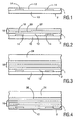
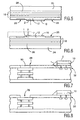
- Figs. 1-8 comprise cross-sectional illustrations of the formation of a semiconductor device with a protective security covering formed thereon. Same reference numbers refer to like elements in the drawings.
- the drawings are diagrammatic and not on scale.
- Fig. 1 illustrate an initial silicon substrate 10 with a first side 1 and a second side 2.
- the substrate 10 comprises a completed integrated circuit wafer structure including a passivation layer 12 in which projected bond pad regions 14.
- the bond pad regions 14 are present at the interface with the silicon substrate 10, or such that they can be exposed from the second side 2 of the substrate 10. This is contarily to the location of the bond pad regions in the prior art, wherein they were present in the top of the interconnect structure, and before being exposed, only being covered by the passivation layer 12.
- the bond pad regions are such defined, that there is no overlap with the transistors on perpendicular projection of the bond pad regions on the substrate.
- a plurality of security coatings 16 is deposited upon the passivation layer 12, the process of the present invention being such that there is no need to etch nor pattern the security coatings 16 and there is no need at this stage for the bond pad regions 14 to be opened.
- the passivation layer 12 may be omitted, but is preferably present.
- the plurality of security coatings forms the protective security covering.
- the security coatings 16 in the illustrated example comprises a Ti02 layer 18, a coating layer 20 based on monoAluminiumPhosphate (MAP) filled with particles of Ti02 and/or TiN, and subsequently a multi alternating layer structure 22 formed of A1 and W layers respectively.
- MAP monoAluminiumPhosphate
- a substrate 24 which can be in the form of a silicon wafer substrate or a glass substrate such as AF45 is attached by means of a layer of glue 26 to the upper surface of the protective coatings 16, and as shown in Fig. 3 .
- the structure is then manipulated and processed in a manner so as to thin the silicon substrate 10 by action against the underside thereof.
- the underside of the structure illustrated in Fig. 4 is then manipulated and processed by means of, for example, a KOH etch at the regions 28 where the bond pads 14 are projected so as to arrive at the structure as illustrated in Fig. 5 .
- Figs. 6 illustrates the structure of Fig. 5 once inverted and the portion 7 illustrated in Fig. 6 is shown in greater detail in Fig. 7 which serves to illustrate a nitride layer 30 provided above the bond pad opening and also part of the semiconductor circuitry 32 provided under the thinned silicon substrate 10 which in accordance with the illustration of Fig. 7 is now oriented above the structure.
- a selective etch is then conducted so as to arrive at the structure as illustrated in Fig. 8 which allows for subsequent testing and packaging of the integrated circuit device as required.
- a substrate transfer technique in accordance with this illustrated embodiment of the present invention proves particularly advantageous in that it allows for the ready processing of the structure in an manner so as to allow for the provision of security coatings formed of substantially inert materials. Also in providing for openings to the bond pad regions through the thinned semiconductor substrate, an appropriate degree of protection due to the density of device structures provided therein is provided and which serves to prevent access to the underside of the structure without fatal damage to the device.
Landscapes
- Engineering & Computer Science (AREA)
- Computer Hardware Design (AREA)
- Physics & Mathematics (AREA)
- General Physics & Mathematics (AREA)
- Microelectronics & Electronic Packaging (AREA)
- Condensed Matter Physics & Semiconductors (AREA)
- Power Engineering (AREA)
- General Engineering & Computer Science (AREA)
- Computer Security & Cryptography (AREA)
- Theoretical Computer Science (AREA)
- Semiconductor Integrated Circuits (AREA)
- Internal Circuitry In Semiconductor Integrated Circuit Devices (AREA)
- Formation Of Insulating Films (AREA)
- Structures Or Materials For Encapsulating Or Coating Semiconductor Devices Or Solid State Devices (AREA)
- Physical Vapour Deposition (AREA)
- Credit Cards Or The Like (AREA)
Claims (10)
- Halbleitergerät, welches eine integrierte Schaltungsstruktur (10) mit einer ersten (1) und einer gegenüberliegenden zweiten Seite (2) aufweist, wobei bei der ersten Seite (1) eine Mehrzahl von Transistoren und Zwischenverbindungen vorhanden ist, wobei die erste Seite mittels einer schützenden Sicherheitsabdeckung (16) abgedeckt ist, wobei die schützende Sicherheitsabdeckung (16) eine im Wesentlichen nicht transparente und im Wesentlichen chemisch inerte Sicherheitsbeschichtung aufweist, wobei das Gerät ferner mit Bondpad-Bereichen (14) bereitgestellt ist,
dadurch gekennzeichnet, dass die Bondpad-Bereiche (14) auf der ersten Oberfläche der schützenden Sicherheitsbeschichtung bei einem Bereich bereitgestellt sind, welcher benachbart der integrierten Schaltungsstruktur (10) ist, und dass die Bondpad-Bereiche (14) von einer Seite des Gerätes zugänglich sind, welche der zweiten Seite der integrierten Schaltungsstruktur (10) entspricht. - Halbleitergerät nach Anspruch 1, dadurch gekennzeichnet, dass die integrierte Schaltungsstruktur (10) ein Siliziumsubstrat ist.
- Halbleitergerät nach Anspruch 1 oder 2, dadurch gekennzeichnet, dass eine weitere Sicherheitsschicht bei der zweiten Seite (2) der Waferstruktur vorhanden ist, wobei die Sicherheitsschicht die Bondpad-Bereiche (14) für einen Zugang dazu exponiert lässt.
- Halbleitergerät nach Anspruch 1, dadurch gekennzeichnet, dass die Bondpad-Bereiche (14) gegen Prüfen mit einem Antiprüfmittel geschützt sind.
- Halbleitergerät nach Anspruch 1, dadurch gekennzeichnet, dass die Sicherheitsbeschichtung (16) eine Schicht von TiO2 aufweist.
- Halbleitergerät nach Anspruch 1, dadurch gekennzeichnet, dass die Sicherheitsbeschichtung (16) aus mehreren alternierenden Schichten gebildet ist, wobei die alternierenden Schichten empfindlich für verschiedene Ätzmittel sind.
- Träger, welcher ein Halbleitergerät gemäß Anspruch 1 aufweist.
- Verfahren eines Herstellens eines Halbleitergeräts, wobei das Verfahren die Schritte aufweist:Bereitstellen eines Halbleitersubstrats (10) mit einer ersten (1) und einer zweiten Seite (2);Bereitstellen einer Struktur von Transistoren und Zwischenverbindungen bei der ersten Seite (1) des Substrats (10), wobei die Struktur Bondpad-Bereiche (14) umfasst, welche auf dem Substrat (10) bereitgestellt sind; undAnwenden einer schützenden Sicherheitsabdeckung (16), welche eine im Wesentlichen nicht transparente und im Wesentlichen chemisch inerte Sicherheitsbeschichtung umfasst,dadurch gekennzeichnet, dass das Verfahren ferner aufweist
Strukturieren des Substrats (10) von der zweiten Seite (2), um so die Bondpad-Bereiche (14) zu exponieren, wobei der verbleibende Teil des Substrats (10) eine integrierte Schaltungsstruktur (10) definiert. - Verfahren nach Anspruch 8, wobei das Substrat dünner gemacht wird und geätzt wird, um die Bondpad-Bereiche (14) zu exponieren.
- Verfahren gemäß Anspruch 8 oder 9, wobei vor dem Gestalten-Schritt ein zweites Substrat (24) auf der schützenden Sicherheitsabdeckung (16) bereitgestellt ist und mittels eines Klebemittels (26) daran angebracht wird.
Priority Applications (1)
| Application Number | Priority Date | Filing Date | Title |
|---|---|---|---|
| EP03744942A EP1490902B1 (de) | 2002-03-21 | 2003-03-20 | Halbleiterbauelement mit einer schutzenden sicherheitsbeschichtung und verfahren zu seiner herstellung |
Applications Claiming Priority (4)
| Application Number | Priority Date | Filing Date | Title |
|---|---|---|---|
| EP02076112 | 2002-03-21 | ||
| EP02076112 | 2002-03-21 | ||
| EP03744942A EP1490902B1 (de) | 2002-03-21 | 2003-03-20 | Halbleiterbauelement mit einer schutzenden sicherheitsbeschichtung und verfahren zu seiner herstellung |
| PCT/IB2003/001025 WO2003081668A1 (en) | 2002-03-21 | 2003-03-20 | Semiconductor device with a protective security coating and method of manufacturing the same |
Publications (2)
| Publication Number | Publication Date |
|---|---|
| EP1490902A1 EP1490902A1 (de) | 2004-12-29 |
| EP1490902B1 true EP1490902B1 (de) | 2010-08-11 |
Family
ID=28051802
Family Applications (1)
| Application Number | Title | Priority Date | Filing Date |
|---|---|---|---|
| EP03744942A Expired - Lifetime EP1490902B1 (de) | 2002-03-21 | 2003-03-20 | Halbleiterbauelement mit einer schutzenden sicherheitsbeschichtung und verfahren zu seiner herstellung |
Country Status (8)
| Country | Link |
|---|---|
| US (1) | US7173323B2 (de) |
| EP (1) | EP1490902B1 (de) |
| JP (1) | JP2005521262A (de) |
| CN (1) | CN100431140C (de) |
| AT (1) | ATE477590T1 (de) |
| AU (1) | AU2003209602A1 (de) |
| DE (1) | DE60333739D1 (de) |
| WO (1) | WO2003081668A1 (de) |
Families Citing this family (6)
| Publication number | Priority date | Publication date | Assignee | Title |
|---|---|---|---|---|
| WO2003046986A2 (en) * | 2001-11-28 | 2003-06-05 | Koninklijke Philips Electronics N.V. | Semiconductor device, and means for checking the authenticity |
| JP2007528121A (ja) * | 2003-07-11 | 2007-10-04 | コーニンクレッカ フィリップス エレクトロニクス エヌ ヴィ | 機密性を要する半導体製品、特にスマートカード・チップ |
| US20080128022A1 (en) * | 2006-11-15 | 2008-06-05 | First Solar, Inc. | Photovoltaic device including a tin oxide protective layer |
| WO2011046769A1 (en) * | 2009-10-14 | 2011-04-21 | Lockheed Martin Corporation | Protective circuit board cover |
| US8947889B2 (en) | 2010-10-14 | 2015-02-03 | Lockheed Martin Corporation | Conformal electromagnetic (EM) detector |
| CN111957664A (zh) * | 2020-07-23 | 2020-11-20 | 伯恩创盛技术研发(惠州)有限公司 | 一种增加玻璃强度的方法及结构 |
Family Cites Families (9)
| Publication number | Priority date | Publication date | Assignee | Title |
|---|---|---|---|---|
| JPS60170239A (ja) * | 1984-02-15 | 1985-09-03 | Nec Corp | 半導体装置 |
| WO1996013858A2 (en) | 1994-10-31 | 1996-05-09 | Philips Electronics N.V. | Integrated microwave semiconductor device with active and passive components |
| US5711987A (en) * | 1996-10-04 | 1998-01-27 | Dow Corning Corporation | Electronic coatings |
| JPH10270583A (ja) * | 1997-03-25 | 1998-10-09 | Nippon Telegr & Teleph Corp <Ntt> | 半導体装置 |
| JP2976917B2 (ja) * | 1997-03-31 | 1999-11-10 | 日本電気株式会社 | 半導体装置 |
| US5808873A (en) * | 1997-05-30 | 1998-09-15 | Motorola, Inc. | Electronic component assembly having an encapsulation material and method of forming the same |
| EP1029347B1 (de) | 1998-06-10 | 2007-02-07 | Koninklijke Philips Electronics N.V. | Halbleiteranordnung mit einer integrierten schaltung und keramischer sicherheitsschicht und verfahren zum herstellen solcher anordnung |
| US6137173A (en) * | 1998-06-30 | 2000-10-24 | Intel Corporation | Preventing backside analysis of an integrated circuit |
| FR2792440B1 (fr) * | 1999-04-19 | 2001-06-08 | Schlumberger Systems & Service | Dispositif a circuit integre securise contre des attaques procedant par destruction controlee d'une couche complementaire |
-
2003
- 2003-03-20 DE DE60333739T patent/DE60333739D1/de not_active Expired - Lifetime
- 2003-03-20 WO PCT/IB2003/001025 patent/WO2003081668A1/en not_active Ceased
- 2003-03-20 JP JP2003579277A patent/JP2005521262A/ja active Pending
- 2003-03-20 AT AT03744942T patent/ATE477590T1/de not_active IP Right Cessation
- 2003-03-20 CN CNB038065630A patent/CN100431140C/zh not_active Expired - Fee Related
- 2003-03-20 EP EP03744942A patent/EP1490902B1/de not_active Expired - Lifetime
- 2003-03-20 US US10/508,745 patent/US7173323B2/en not_active Expired - Lifetime
- 2003-03-20 AU AU2003209602A patent/AU2003209602A1/en not_active Abandoned
Also Published As
| Publication number | Publication date |
|---|---|
| AU2003209602A1 (en) | 2003-10-08 |
| JP2005521262A (ja) | 2005-07-14 |
| WO2003081668A1 (en) | 2003-10-02 |
| US20050140003A1 (en) | 2005-06-30 |
| ATE477590T1 (de) | 2010-08-15 |
| US7173323B2 (en) | 2007-02-06 |
| EP1490902A1 (de) | 2004-12-29 |
| DE60333739D1 (de) | 2010-09-23 |
| CN1643681A (zh) | 2005-07-20 |
| CN100431140C (zh) | 2008-11-05 |
Similar Documents
| Publication | Publication Date | Title |
|---|---|---|
| US12176303B2 (en) | Wafer-level bonding of obstructive elements | |
| US6762510B2 (en) | Flexible integrated monolithic circuit | |
| EP1155452B1 (de) | Halbleiteranordnung mit sicherheitsbeschichtung und chipkarte mit einer solchen anordnung | |
| KR101022641B1 (ko) | 가요성 집적 회로 및 시스템 | |
| EP1437695B1 (de) | Chipkarte und diese Chipkarte verwendendes Kontensystem | |
| CN101151544A (zh) | 半导体器件、其制造方法、及其测量方法 | |
| US8330191B2 (en) | Intrusion protection using stress changes | |
| JP2003269906A (ja) | 容量検出型センサ及びその製造方法 | |
| KR20050062412A (ko) | 반도체 집적 회로, 반도체 장치, 및 반도체 집적 회로의제조 방법 | |
| CN102082145B (zh) | 晶片及其形成方法 | |
| EP1490902B1 (de) | Halbleiterbauelement mit einer schutzenden sicherheitsbeschichtung und verfahren zu seiner herstellung | |
| JP2000124162A (ja) | 半導体装置の製造方法 | |
| EP1029347B1 (de) | Halbleiteranordnung mit einer integrierten schaltung und keramischer sicherheitsschicht und verfahren zum herstellen solcher anordnung | |
| JP3400329B2 (ja) | 半導体装置 | |
| JP2000011129A (ja) | Icカードおよびその製造方法 | |
| JP4386570B2 (ja) | 安全集積回路デバイスとその製造方法 | |
| US6137173A (en) | Preventing backside analysis of an integrated circuit | |
| JP4690561B2 (ja) | 半導体チップ | |
| US7088006B2 (en) | Integrated circuit arrangement | |
| CN112201574A (zh) | 多层晶圆键合方法 | |
| US20230029248A1 (en) | Chip module and method for forming a chip module | |
| JPH11144019A (ja) | Icカード | |
| JP2000112825A (ja) | 半導体装置 | |
| JP2003037030A (ja) | 半導体装置 | |
| JP2006186328A (ja) | 半導体装置およびその作製方法 |
Legal Events
| Date | Code | Title | Description |
|---|---|---|---|
| PUAI | Public reference made under article 153(3) epc to a published international application that has entered the european phase |
Free format text: ORIGINAL CODE: 0009012 |
|
| 17P | Request for examination filed |
Effective date: 20041021 |
|
| AK | Designated contracting states |
Kind code of ref document: A1 Designated state(s): AT BE BG CH CY CZ DE DK EE ES FI FR GB GR HU IE IT LI LU MC NL PT RO SE SI SK TR |
|
| AX | Request for extension of the european patent |
Extension state: AL LT LV MK |
|
| RAP1 | Party data changed (applicant data changed or rights of an application transferred) |
Owner name: NXP B.V. |
|
| 17Q | First examination report despatched |
Effective date: 20080708 |
|
| GRAP | Despatch of communication of intention to grant a patent |
Free format text: ORIGINAL CODE: EPIDOSNIGR1 |
|
| RIC1 | Information provided on ipc code assigned before grant |
Ipc: H01L 23/28 20060101ALI20100212BHEP Ipc: H01L 23/58 20060101AFI20100212BHEP Ipc: G06K 19/073 20060101ALI20100212BHEP |
|
| GRAS | Grant fee paid |
Free format text: ORIGINAL CODE: EPIDOSNIGR3 |
|
| GRAA | (expected) grant |
Free format text: ORIGINAL CODE: 0009210 |
|
| AK | Designated contracting states |
Kind code of ref document: B1 Designated state(s): AT BE BG CH CY CZ DE DK EE ES FI FR GB GR HU IE IT LI LU MC NL PT RO SE SI SK TR |
|
| REG | Reference to a national code |
Ref country code: GB Ref legal event code: FG4D |
|
| REG | Reference to a national code |
Ref country code: CH Ref legal event code: EP |
|
| REG | Reference to a national code |
Ref country code: IE Ref legal event code: FG4D |
|
| REF | Corresponds to: |
Ref document number: 60333739 Country of ref document: DE Date of ref document: 20100923 Kind code of ref document: P |
|
| REG | Reference to a national code |
Ref country code: NL Ref legal event code: VDEP Effective date: 20100811 |
|
| PG25 | Lapsed in a contracting state [announced via postgrant information from national office to epo] |
Ref country code: NL Free format text: LAPSE BECAUSE OF FAILURE TO SUBMIT A TRANSLATION OF THE DESCRIPTION OR TO PAY THE FEE WITHIN THE PRESCRIBED TIME-LIMIT Effective date: 20100811 Ref country code: AT Free format text: LAPSE BECAUSE OF FAILURE TO SUBMIT A TRANSLATION OF THE DESCRIPTION OR TO PAY THE FEE WITHIN THE PRESCRIBED TIME-LIMIT Effective date: 20100811 Ref country code: FI Free format text: LAPSE BECAUSE OF FAILURE TO SUBMIT A TRANSLATION OF THE DESCRIPTION OR TO PAY THE FEE WITHIN THE PRESCRIBED TIME-LIMIT Effective date: 20100811 |
|
| PG25 | Lapsed in a contracting state [announced via postgrant information from national office to epo] |
Ref country code: BG Free format text: LAPSE BECAUSE OF FAILURE TO SUBMIT A TRANSLATION OF THE DESCRIPTION OR TO PAY THE FEE WITHIN THE PRESCRIBED TIME-LIMIT Effective date: 20101111 Ref country code: SI Free format text: LAPSE BECAUSE OF FAILURE TO SUBMIT A TRANSLATION OF THE DESCRIPTION OR TO PAY THE FEE WITHIN THE PRESCRIBED TIME-LIMIT Effective date: 20100811 Ref country code: PT Free format text: LAPSE BECAUSE OF FAILURE TO SUBMIT A TRANSLATION OF THE DESCRIPTION OR TO PAY THE FEE WITHIN THE PRESCRIBED TIME-LIMIT Effective date: 20101213 Ref country code: CY Free format text: LAPSE BECAUSE OF FAILURE TO SUBMIT A TRANSLATION OF THE DESCRIPTION OR TO PAY THE FEE WITHIN THE PRESCRIBED TIME-LIMIT Effective date: 20100811 |
|
| PG25 | Lapsed in a contracting state [announced via postgrant information from national office to epo] |
Ref country code: SE Free format text: LAPSE BECAUSE OF FAILURE TO SUBMIT A TRANSLATION OF THE DESCRIPTION OR TO PAY THE FEE WITHIN THE PRESCRIBED TIME-LIMIT Effective date: 20100811 Ref country code: BE Free format text: LAPSE BECAUSE OF FAILURE TO SUBMIT A TRANSLATION OF THE DESCRIPTION OR TO PAY THE FEE WITHIN THE PRESCRIBED TIME-LIMIT Effective date: 20100811 Ref country code: GR Free format text: LAPSE BECAUSE OF FAILURE TO SUBMIT A TRANSLATION OF THE DESCRIPTION OR TO PAY THE FEE WITHIN THE PRESCRIBED TIME-LIMIT Effective date: 20101112 |
|
| PG25 | Lapsed in a contracting state [announced via postgrant information from national office to epo] |
Ref country code: DK Free format text: LAPSE BECAUSE OF FAILURE TO SUBMIT A TRANSLATION OF THE DESCRIPTION OR TO PAY THE FEE WITHIN THE PRESCRIBED TIME-LIMIT Effective date: 20100811 |
|
| PG25 | Lapsed in a contracting state [announced via postgrant information from national office to epo] |
Ref country code: CZ Free format text: LAPSE BECAUSE OF FAILURE TO SUBMIT A TRANSLATION OF THE DESCRIPTION OR TO PAY THE FEE WITHIN THE PRESCRIBED TIME-LIMIT Effective date: 20100811 Ref country code: RO Free format text: LAPSE BECAUSE OF FAILURE TO SUBMIT A TRANSLATION OF THE DESCRIPTION OR TO PAY THE FEE WITHIN THE PRESCRIBED TIME-LIMIT Effective date: 20100811 Ref country code: IT Free format text: LAPSE BECAUSE OF FAILURE TO SUBMIT A TRANSLATION OF THE DESCRIPTION OR TO PAY THE FEE WITHIN THE PRESCRIBED TIME-LIMIT Effective date: 20100811 Ref country code: EE Free format text: LAPSE BECAUSE OF FAILURE TO SUBMIT A TRANSLATION OF THE DESCRIPTION OR TO PAY THE FEE WITHIN THE PRESCRIBED TIME-LIMIT Effective date: 20100811 Ref country code: SK Free format text: LAPSE BECAUSE OF FAILURE TO SUBMIT A TRANSLATION OF THE DESCRIPTION OR TO PAY THE FEE WITHIN THE PRESCRIBED TIME-LIMIT Effective date: 20100811 |
|
| PLBE | No opposition filed within time limit |
Free format text: ORIGINAL CODE: 0009261 |
|
| STAA | Information on the status of an ep patent application or granted ep patent |
Free format text: STATUS: NO OPPOSITION FILED WITHIN TIME LIMIT |
|
| PG25 | Lapsed in a contracting state [announced via postgrant information from national office to epo] |
Ref country code: ES Free format text: LAPSE BECAUSE OF FAILURE TO SUBMIT A TRANSLATION OF THE DESCRIPTION OR TO PAY THE FEE WITHIN THE PRESCRIBED TIME-LIMIT Effective date: 20101122 |
|
| 26N | No opposition filed |
Effective date: 20110512 |
|
| REG | Reference to a national code |
Ref country code: DE Ref legal event code: R097 Ref document number: 60333739 Country of ref document: DE Effective date: 20110512 |
|
| PG25 | Lapsed in a contracting state [announced via postgrant information from national office to epo] |
Ref country code: MC Free format text: LAPSE BECAUSE OF NON-PAYMENT OF DUE FEES Effective date: 20110331 |
|
| REG | Reference to a national code |
Ref country code: CH Ref legal event code: PL |
|
| REG | Reference to a national code |
Ref country code: IE Ref legal event code: MM4A |
|
| PG25 | Lapsed in a contracting state [announced via postgrant information from national office to epo] |
Ref country code: LI Free format text: LAPSE BECAUSE OF NON-PAYMENT OF DUE FEES Effective date: 20110331 Ref country code: CH Free format text: LAPSE BECAUSE OF NON-PAYMENT OF DUE FEES Effective date: 20110331 Ref country code: IE Free format text: LAPSE BECAUSE OF NON-PAYMENT OF DUE FEES Effective date: 20110320 |
|
| PGFP | Annual fee paid to national office [announced via postgrant information from national office to epo] |
Ref country code: FR Payment date: 20120410 Year of fee payment: 10 |
|
| PGFP | Annual fee paid to national office [announced via postgrant information from national office to epo] |
Ref country code: DE Payment date: 20120223 Year of fee payment: 10 |
|
| PGFP | Annual fee paid to national office [announced via postgrant information from national office to epo] |
Ref country code: GB Payment date: 20120224 Year of fee payment: 10 |
|
| PG25 | Lapsed in a contracting state [announced via postgrant information from national office to epo] |
Ref country code: LU Free format text: LAPSE BECAUSE OF NON-PAYMENT OF DUE FEES Effective date: 20110320 |
|
| PG25 | Lapsed in a contracting state [announced via postgrant information from national office to epo] |
Ref country code: TR Free format text: LAPSE BECAUSE OF FAILURE TO SUBMIT A TRANSLATION OF THE DESCRIPTION OR TO PAY THE FEE WITHIN THE PRESCRIBED TIME-LIMIT Effective date: 20100811 |
|
| PG25 | Lapsed in a contracting state [announced via postgrant information from national office to epo] |
Ref country code: HU Free format text: LAPSE BECAUSE OF FAILURE TO SUBMIT A TRANSLATION OF THE DESCRIPTION OR TO PAY THE FEE WITHIN THE PRESCRIBED TIME-LIMIT Effective date: 20100811 |
|
| GBPC | Gb: european patent ceased through non-payment of renewal fee |
Effective date: 20130320 |
|
| REG | Reference to a national code |
Ref country code: FR Ref legal event code: ST Effective date: 20131129 |
|
| REG | Reference to a national code |
Ref country code: DE Ref legal event code: R119 Ref document number: 60333739 Country of ref document: DE Effective date: 20131001 |
|
| PG25 | Lapsed in a contracting state [announced via postgrant information from national office to epo] |
Ref country code: FR Free format text: LAPSE BECAUSE OF NON-PAYMENT OF DUE FEES Effective date: 20130402 Ref country code: GB Free format text: LAPSE BECAUSE OF NON-PAYMENT OF DUE FEES Effective date: 20130320 Ref country code: DE Free format text: LAPSE BECAUSE OF NON-PAYMENT OF DUE FEES Effective date: 20131001 |