EP1484947A2 - Ansteuerschaltung für den Betrieb mindestens einer Lampe in einem dazugehörigen Lastkreis - Google Patents
Ansteuerschaltung für den Betrieb mindestens einer Lampe in einem dazugehörigen Lastkreis Download PDFInfo
- Publication number
- EP1484947A2 EP1484947A2 EP04009454A EP04009454A EP1484947A2 EP 1484947 A2 EP1484947 A2 EP 1484947A2 EP 04009454 A EP04009454 A EP 04009454A EP 04009454 A EP04009454 A EP 04009454A EP 1484947 A2 EP1484947 A2 EP 1484947A2
- Authority
- EP
- European Patent Office
- Prior art keywords
- control
- bipolar transistor
- circuit
- field effect
- effect transistor
- Prior art date
- Legal status (The legal status is an assumption and is not a legal conclusion. Google has not performed a legal analysis and makes no representation as to the accuracy of the status listed.)
- Granted
Links
Images

Classifications
-
- H—ELECTRICITY
- H05—ELECTRIC TECHNIQUES NOT OTHERWISE PROVIDED FOR
- H05B—ELECTRIC HEATING; ELECTRIC LIGHT SOURCES NOT OTHERWISE PROVIDED FOR; CIRCUIT ARRANGEMENTS FOR ELECTRIC LIGHT SOURCES, IN GENERAL
- H05B41/00—Circuit arrangements or apparatus for igniting or operating discharge lamps
- H05B41/14—Circuit arrangements
- H05B41/26—Circuit arrangements in which the lamp is fed by power derived from DC by means of a converter, e.g. by high-voltage DC
- H05B41/28—Circuit arrangements in which the lamp is fed by power derived from DC by means of a converter, e.g. by high-voltage DC using static converters
- H05B41/282—Circuit arrangements in which the lamp is fed by power derived from DC by means of a converter, e.g. by high-voltage DC using static converters with semiconductor devices
-
- H—ELECTRICITY
- H05—ELECTRIC TECHNIQUES NOT OTHERWISE PROVIDED FOR
- H05B—ELECTRIC HEATING; ELECTRIC LIGHT SOURCES NOT OTHERWISE PROVIDED FOR; CIRCUIT ARRANGEMENTS FOR ELECTRIC LIGHT SOURCES, IN GENERAL
- H05B41/00—Circuit arrangements or apparatus for igniting or operating discharge lamps
- H05B41/14—Circuit arrangements
- H05B41/26—Circuit arrangements in which the lamp is fed by power derived from DC by means of a converter, e.g. by high-voltage DC
- H05B41/28—Circuit arrangements in which the lamp is fed by power derived from DC by means of a converter, e.g. by high-voltage DC using static converters
- H05B41/282—Circuit arrangements in which the lamp is fed by power derived from DC by means of a converter, e.g. by high-voltage DC using static converters with semiconductor devices
- H05B41/2825—Circuit arrangements in which the lamp is fed by power derived from DC by means of a converter, e.g. by high-voltage DC using static converters with semiconductor devices by means of a bridge converter in the final stage
Definitions
- the present invention relates to a control circuit for the operation of at least one Lamp in an associated load circuit, in which the connections for the at least one Lamp are arranged with two switches in a half-bridge arrangement.
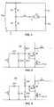
- FIG. 1 Such a control circuit known from the prior art is shown schematically in FIG. 1.
- the so-called intermediate circuit voltage U zw is present on the input side.
- This is a DC voltage that is usually generated from the mains voltage using circuits familiar to those skilled in the art.
- Two switches S1, S2 are arranged in series in a half-bridge arrangement and are controlled via a respective input circuit E1, E2, not shown.
- the connection point of the two switches is connected via a choke L to the lamp La, through which the lamp current I L flows during operation.
- the two coupling capacitors C K1 , C K2 complete the circuit.
- Alternative circuit structures are familiar to the person skilled in the art, but are not described in more detail below, since they are irrelevant for the implementation of the invention.
- the switches S1, S2 When used in the so-called medium voltage range, the switches S1, S2 must be designed to switch voltages between 400 and 1000 volts.
- the switching frequency is in the order of 40 to 50 kHz.
- the duty cycle of the circuit shown in Figure 1 is 50 percent.
- the network power to be switched is more than 100 watts.
- MOSFETs metal oxide semiconductor field effect transistors
- IGBTs insulated gate bipolar transistors
- the IGBTs have large transmission losses.
- components designed for such boundary conditions are cheaper because they require less chip area, but their poor dynamic switching behavior has a negative effect. Since the collector current cannot be switched off quickly enough, the switching overlaps with the collector-emitter voltage result in high switching losses.
- the present invention is therefore based on the object of a generic control circuit to develop in such a way that they operate at medium currents of approx. 1 to 10 amperes has low transmission losses, at the same time low costs and given controllability from microcontrollers or integrated control modules.
- the present invention is based on the knowledge that a fast Switching can be achieved when combined with a low voltage MOSFET a bipolar transistor is used.
- the MOSFET therefore only needs the small control voltage for the bipolar transistor and can therefore be designed small and cheap become.
- the bipolar transistor whose power loss is only linear with the one flowing through it When electricity is linked, it can be dimensioned at low cost for large currents. This is the advantage of the MOSFET - high dynamics and controllability from an integrated Circuit and that of the bipolar transistor - large, processable at an affordable price Performance - optimally linked.
- the second finding on which the invention is based is that such Control circuit can be started easily if part of the in the load circuit flowing energy is transferred to the input circuit of the respective switch. Since it is a bipolar transistor is essentially a current-controlled component, A corresponding control current must be made available to him at the base. To do this a primary winding of a transformer is formed in the load circuit, its secondary windings are arranged in the input circuit of each bipolar transistor and thus the base of the bipolar transistor supply with electricity. To reduce the conduction losses of the bipolar transistors it is preferred to dimension the transformer so that the base current is approx Makes up a fifth of the collector current. With a practical current gain of 20 the bipolar transistor is overdriven by a factor of 4. This results in low transmission losses. While driving the bipolar transistor as a result of the large required Control currents from an integrated circuit would not be possible, this is the case with the MOSFET an essentially voltage-controlled component is very possible.
- Cascode circuits with a bipolar transistor and a are from the prior art MOSFET transistor known, but which are used for completely different purposes: So is it is known from EP 0 753 987 D1, such a cascode circuit in which the bipolar transistors controlled by MOSFETS arranged in the emitter, for switching off to use a half-bridge arrangement when the lamp to be operated has aged.
- EP 0 753 987 D1 such a cascode circuit in which the bipolar transistors controlled by MOSFETS arranged in the emitter, for switching off to use a half-bridge arrangement when the lamp to be operated has aged.
- FIG. 4 there, is also a cascode circuit of this type used, but here lies a constant due to the different purpose Voltage at the base of the bipolar transistor 20 on.
- Figure 6 is also such a cascode circuit is shown, but in contrast to the present Invention, no defined magnetic reversal of the transformer takes place.
- the duty cycle of the two switches is Half bridge is essentially 50 percent, ensuring that the transformer is not goes into saturation because it is remagnetized by the other transistor current.
- a preferred embodiment of the present invention is characterized in that that a diode is arranged such that it turns on in the case of an npn bipolar transistor Outflow of a positive base current through the secondary winding, in the case of a pnp bipolar transistor an outflow of a negative base current through the secondary winding prevented.
- This is important because the base current flows through the secondary winding the formation of a voltage between the control electrode of the bipolar transistor and would prevent the reference electrode of the field effect transistor and thus the Formation of a sufficiently high base-emitter voltage.
- Parallel to the control electrode of the Bipolar transistor and the reference electrode of the field effect transistor can be at least one Diode or a zener diode between the potential of the control electrode of the bipolar transistor and the potential of the reference electrode of the field effect transistor.
- a Zener diode In order to is at least the voltage at the pn junction of the diode as the base-emitter voltage at the pn junction of the bipolar transistor. An opening of the bipolar transistor can thus be ensured. The same applies when using a Zener diode.
- Parallel to the control electrode of the bipolar transistor and the reference electrode of the field effect transistor is also preferably a series connection of an ohmic resistor and a capacitor arranged. This is a simple and inexpensive way to start implement the control circuit according to the invention. Detailed information on this follow below.
- the control electrode of the field effect transistor is preferred with a integrated driver circuit connected. As already mentioned, it is one Field effect transistor around a voltage-controlled element, which is due to the low requirement can be controlled at control current from an integrated circuit.
- the diode or the zener diode, which is parallel to the control electrode of the bipolar transistor and the reference electrode of the field effect transistor between the potential of the control electrode of the bipolar transistor and the potential of the reference electrode of the field effect transistor is preferably dimensioned such that a voltage of at least 1 volt, preferably, is applied to it approx. 2 volts, drops.
- the reference electrode of the field effect transistor of each switch is preferably a first Reference potential connected while the control electrode of the bipolar transistor of each switch is connected to a second reference potential via a high-resistance resistor.
- This resistor is used to supply charge carriers to the base of the bipolar transistor, as long as the secondary winding of the transformer has no charge carriers in the Introduces input circle, especially at the start.
- bipolar transistor It is also preferred between the control and the reference electrode of the bipolar transistor an ohmic resistor is arranged on each switch. This ensures that the transistor is not switched on at the wrong time by interference pulses when switched off. In a Cascode circuit as here, it can also be used to charge or discharge parasitic Capacities of the field effect transistor serve. Finally, it also increases the dielectric strength of bipolar transistors.
- the switches are preferably designed such that they operate at a frequency between 100 Hz and 300 kHz and a voltage of 100 to 1000 volts can be operated. Further advantageous embodiments result from the subclaims.
- FIGS 2 and 3 show embodiments of the input circuit E2 of Figure 1 in a drive circuit according to the invention. Identical components are provided with the same reference symbols and are only explained once.
- a bipolar transistor B2 and a field effect transistor F2 in a cascode arrangement form the switch S2.
- the gate of the field effect transistor F2 is connected via its connection 10 to the output of an integrated driver circuit.
- a transformer preferably designed as a toroid, is located in the load circuit with its primary winding L 0 . Secondary windings are arranged in the respective input circuit, in the present case the secondary winding L2 in the input circuit E2.
- a diode D21 prevents charge carriers from flowing out of the base via the secondary winding L2.
- a high-resistance resistor R21 which is connected on the one hand to the base of the bipolar transistor B2, and on the other hand with the intermediate circuit voltage U zw , charge carriers can be provided on the base.
- the base of the bipolar transistor is connected to the reference potential via a parallel connection of a diode D22 and, on the other hand, via a parallel connection of a diode D22 and a resistor R22, on which the reference electrode of the field effect transistor F2 is located. This allows a sufficiently large base-emitter voltage to be generated with which the circuit arrangement can be started.
- a resistor R23 is used to withstand the voltage of the associated bipolar transistor.
- a typical value for R21 is 1 M ⁇ , a typical value for R22 is 100 ⁇ .
- Diode D22 can also provide a Zener diode, of course in reverse order his.
- the series circuit comprising secondary winding L2 and diode D21 is connected in parallel with a Zener diode Z2 on the one hand, and the series circuit with a resistor R22 and a capacitor C2 on the other hand.
- the base of the transistor is in turn connected to the intermediate circuit voltage U zw via a high-resistance resistor R21 and to the working electrode of the field effect transistor F2 via a resistor R23.
- the Zener diode Z2 dimensioned to two volts
- the field effect transistor F2 is switched on via a suitable signal at the connection 10, which opens the bipolar transistor B2
- the capacitor C2 discharges and leads to a base current I B of 100 mA when the resistor R22 is dimensioned to 10 ⁇ .
- the switch S2 is switched on for one to two microseconds, a load current I L begins to flow and a signal is coupled into the input circuit E2 by linking primary winding L 0 and secondary winding L2, as a result of which the circuit arrangement is started.
- the switch-off behavior of the circuit is also improved by this solution.
- the problem is that when the field effect transistor F2 is switched off, the emitter current I E of the bipolar transistor suddenly goes to zero.
- the collector current I C wants to continue to flow, the base is flooded with charge carriers, which leads to long switch-off times. Long switch-off times are associated with the problem that the collector current I C and collector-emitter voltage U CE have positive values over a certain period of time. Since the product of these two sizes dominates the transmission loss, this results in undesirably high power losses.
- a downsider C2 in the embodiment according to FIG. 3 becomes a on the base side low-resistance branch provided to ground.
- the collector current I C can therefore continue to flow to the ground almost unhindered after the field effect transistor F2 has been switched off as a negative base current -I B. This results in fast switch-off times.
- the resistor R23 is dimensioned, for example, with 100 ⁇ and serves to ensure that no current can flow out as long as the field effect transistor is high-resistance.
- Figures 2 and 3 show an example of the input circuit E2. It is obvious to the person skilled in the art that the input circuit E1 should be designed symmetrically for this in a corresponding manner is.
Landscapes
- Electronic Switches (AREA)
- Circuit Arrangements For Discharge Lamps (AREA)
Abstract
Description
- Figur 1
- in schematischer Darstellung ein Prinzipschaltbild mit einer aus einer Halbbrückenschaltung angesteuerten Lampe;
- Figur 2
- ein erstes Ausführungsbeispiel eines Eingangskreises einer erfindungsgemäßen Ansteuerschaltung;
- Figur 3
- ein zweites Ausführungsbeispiel eines Eingangskreises einer erfindungsgemäßen Ansteuerschaltung; und
- Figur 4
- den zeitlichen Verlauf des Basisstroms, des Kollektorstroms und der Kollektor-Emitter-Spannung bei einem Abschaltvorgang des Schalters der Halbbrückenanordnung in einer erfindungsgemäßen Ansteuerschaltung.
Claims (10)
- Ansteuerschaltung für den Betrieb mindestens einer Lampe (La) in einem dazugehörigen Lastkreis, in dem die Anschlüsse für die mindestens eine Lampe angeordnet sind, mit zwei Schaltern (S1, S2) in Halbbrückenanordnung, wobei jeder Schalter (S1, S2) in Kaskodeschaltung einen Bipolartransistor (B2) mit einer Steuer-, einer Arbeits- und einer Bezugselektrode und einen Feldeffekttransistor (F2) mit einer Steuer-, einer Arbeits- und einer Bezugselektrode umfasst, wobei der Mittelpunkt der Halbbrückenanordnung mit dem mindestens einen Lastkreis gekoppelt ist, und jede derartige Kaskodeschaltung einen Eingangskreis (E1, E2) aufweist, in dem parallel zur Steuerelektrode des Bipolartransistors (B2) und der Bezugselektrode des Feldeffekttransistors (F2) die Serienschaltung einer Diode (D21) und einer Sekundärwicklung (L2) eines Übertragers angeordnet ist, dessen Primärwicklung (L0) derart im Lastkreis angeordnet ist, dass sie im Betrieb der mindestens einen Lampe (La) vom Lastkreisstrom (IL) durchflossen wird.
- Ansteuerschaltung nach Anspruch 1,
dadurch gekennzeichnet, dass die Diode (D21) derart angeordnet ist, dass sie im Falle eines npn-Bipolartransistors (B2) ein Abfließen eines positiven Basisstromes (IB) über die Sekundärwicklung (L2), im Falle eines pnp-Bipolartransistors ein Abfließen eines negativen Basisstromes über die Sekundärwicklung verhindert. - Ansteuerschaltung nach einem der Ansprüche 1 oder 2,
dadurch gekennzeichnet, dass parallel zur Steuerelektrode des Bipolartransistors (B2) und der Bezugselektrode des Feldeffekttransistors (F2) mindestens eine Diode (D22) oder eine Zenerdiode (Z2) zwischen dem Potential der Steuerelektrode des Bipolartransistors (B2) und dem Potential der Bezugselektrode des Feldeffekttransistors (F2) angeordnet ist. - Ansteuerschaltung nach einem der vorhergehenden Ansprüche,
dadurch gekennzeichnet, dass parallel zur Steuerelektrode des Bipolartransistors (B2) und der Bezugselektrode des Feldeffekttransistors (F2) eine Serienschaltung eines ohmschen Widerstandes (R22) und eines Kondensators (C2) angeordnet ist. - Ansteuerschaltung nach einem der vorhergehenden Ansprüche,
dadurch gekennzeichnet, dass die Steuerelektrode des Feldeffekttransistors (F2) mit einer integrierten Treiberschaltung verbunden ist. - Ansteuerschaltung nach einem der vorhergehenden Ansprüche,
dadurch gekennzeichnet, dass der Duty-Cycle der beiden Schalter (S1, S2) der Halbbrücke im wesentlichen 50 Prozent beträgt. - Ansteuerschaltung nach einem der Ansprüche 3 bis 6,
dadurch gekennzeichnet, dass die Diode (D22) oder die Zenerdiode (Z2) so bemessen ist, dass an ihr eine Spannung von mindestens 1 V, bevorzugt ca. 2 V, abfällt. - Ansteuerschaltung nach einem der vorhergehenden Ansprüche,
dadurch gekennzeichnet, dass die Bezugselektrode des Feldeffekttransistors (F2) jedes Schalters (S1, S2) mit einem ersten Bezugspotential verbunden ist und die Steuerelektrode des Bipolartransistors mindestens eines Schalters über einen hochohmigen Widerstand (R21) mit einem zweiten Bezugspotential (UZW). - Ansteuerschaltung nach einem der vorhergehenden Ansprüche,
dadurch gekennzeichnet, dass zwischen der Steuer- und der Bezugselektrode des Bipolartransistors (B2) jedes Schalters (S1, S2) ein ohmscher Widerstand (R23) angeordnet ist. - Ansteuerschaltung nach einem der vorhergehenden Ansprüche,
dadurch gekennzeichnet, dass die Schalter (S1, S2) ausgelegt sind, im Betrieb mit einer Frequenz zwischen 100 Hz und 300 kHz und einer Spannung von 100 bis 1000 V betrieben zu werden.
Applications Claiming Priority (2)
| Application Number | Priority Date | Filing Date | Title |
|---|---|---|---|
| DE10325872A DE10325872A1 (de) | 2003-06-06 | 2003-06-06 | Ansteuerschaltung für den Betrieb mindestens einer Lampe in einem dazugehörigen Lastkreis |
| DE10325872 | 2003-06-06 |
Publications (3)
| Publication Number | Publication Date |
|---|---|
| EP1484947A2 true EP1484947A2 (de) | 2004-12-08 |
| EP1484947A3 EP1484947A3 (de) | 2006-01-18 |
| EP1484947B1 EP1484947B1 (de) | 2009-08-19 |
Family
ID=33154586
Family Applications (1)
| Application Number | Title | Priority Date | Filing Date |
|---|---|---|---|
| EP04009454A Expired - Lifetime EP1484947B1 (de) | 2003-06-06 | 2004-04-21 | Ansteuerschaltung für den Betrieb mindestens einer Lampe in einem dazugehörigen Lastkreis |
Country Status (7)
| Country | Link |
|---|---|
| US (1) | US7057355B2 (de) |
| EP (1) | EP1484947B1 (de) |
| KR (1) | KR20040105592A (de) |
| CN (1) | CN100574549C (de) |
| CA (1) | CA2469575A1 (de) |
| DE (2) | DE10325872A1 (de) |
| TW (1) | TW200503584A (de) |
Families Citing this family (1)
| Publication number | Priority date | Publication date | Assignee | Title |
|---|---|---|---|---|
| DE102012112391B4 (de) * | 2012-12-17 | 2018-10-04 | Phoenix Contact Gmbh & Co. Kg | Schaltnetzteil mit einer Kaskodenschaltung |
Family Cites Families (8)
| Publication number | Priority date | Publication date | Assignee | Title |
|---|---|---|---|---|
| US4894587A (en) * | 1984-08-17 | 1990-01-16 | Lutron Electronics Co., Inc. | High frequency gas discharge lamp dimming ballast |
| FR2603756B1 (fr) * | 1986-09-09 | 1993-03-26 | Cfei Co Fr Electrotherm Ind | Onduleur de tension autopilote en frequence |
| CA2118933C (en) * | 1992-07-17 | 1998-05-05 | John G. Konopka | Power supply circuit |
| TW307980B (de) * | 1994-04-28 | 1997-06-11 | Toshiba Light Technic Kk | |
| US5783911A (en) * | 1995-07-12 | 1998-07-21 | Patent-Treuhand-Gesellschaft Fuer Elektrische Gluehlampen Mbh | Circuit arrangement for operating electric lamps, and operating method for electric lamps |
| EP0936845B1 (de) * | 1998-02-10 | 2002-09-18 | STMicroelectronics S.A. | Gerät und Verfahren zum Zünden und Betreiben einer Leuchtstofflampe |
| DE19830368A1 (de) * | 1998-07-07 | 2000-02-03 | Patent Treuhand Ges Fuer Elektrische Gluehlampen Mbh | Elektronisches Vorschaltgerät mit Einschaltstrombegrenzung |
| DE10200047A1 (de) * | 2002-01-02 | 2003-07-17 | Patent Treuhand Ges Fuer Elektrische Gluehlampen Mbh | Vorschaltgerät für eine Lampe und Verfahren zum betreiben eines Vorschaltgeräts für eine Lampe |
-
2003
- 2003-06-06 DE DE10325872A patent/DE10325872A1/de not_active Withdrawn
-
2004
- 2004-04-21 EP EP04009454A patent/EP1484947B1/de not_active Expired - Lifetime
- 2004-04-21 DE DE502004009910T patent/DE502004009910D1/de not_active Expired - Lifetime
- 2004-05-06 TW TW093112716A patent/TW200503584A/zh unknown
- 2004-05-24 US US10/851,227 patent/US7057355B2/en not_active Expired - Fee Related
- 2004-06-02 CA CA002469575A patent/CA2469575A1/en not_active Abandoned
- 2004-06-05 KR KR1020040041155A patent/KR20040105592A/ko not_active Abandoned
- 2004-06-07 CN CNB2004100484862A patent/CN100574549C/zh not_active Expired - Fee Related
Also Published As
| Publication number | Publication date |
|---|---|
| US20040245938A1 (en) | 2004-12-09 |
| CA2469575A1 (en) | 2004-12-06 |
| CN100574549C (zh) | 2009-12-23 |
| US7057355B2 (en) | 2006-06-06 |
| EP1484947B1 (de) | 2009-08-19 |
| EP1484947A3 (de) | 2006-01-18 |
| DE502004009910D1 (de) | 2009-10-01 |
| TW200503584A (en) | 2005-01-16 |
| CN1575079A (zh) | 2005-02-02 |
| DE10325872A1 (de) | 2004-12-23 |
| KR20040105592A (ko) | 2004-12-16 |
Similar Documents
| Publication | Publication Date | Title |
|---|---|---|
| EP2232950B1 (de) | Buck-konverter und verfahren zum bereitstellen eines stroms für mindestens eine led | |
| EP2232686B1 (de) | Buck-konverter zum bereitstellen eines stroms für mindestens eine led | |
| DE112012001674T5 (de) | Kaskodenschalter mit selbstsperrenden und selbstleitenden Bauelementen und die Schalter umfassende Schaltungen | |
| EP0108283A2 (de) | Elektronischer Schalter | |
| DE19746112A1 (de) | Stromrichteranordnung | |
| DE3878655T2 (de) | Dc-ac-brueckenschaltung. | |
| DE102014106417A1 (de) | Systeme und Verfahren zum Eliminieren von Übergangsverlusten in DC-DC-Wandlern | |
| DE102016216993A1 (de) | Bootstrap-Kompensierungsschaltung und Leistungsmodul | |
| DE2320128B2 (de) | Zerhacker | |
| EP1783910B1 (de) | Schaltungsanordnung und ein Verfahren zur galvanisch getrennten Ansteuerung eines Halbleiterschalters | |
| DE10229633A1 (de) | Ansteuerung für einen Halbbrückenwechselrichter | |
| EP0155059A2 (de) | Schaltungsanordnung zum Schalten des Stromes in einer induktiven Last | |
| DE1952576A1 (de) | Schaltvorrichtung fuer einen Lastkreis | |
| DE3813672C2 (de) | Wechselrichter für eine induktive Last | |
| DE60316105T2 (de) | Ansteuerschaltung für einen Steueranschluss eines Bipolartransistors mit geschaltetem und einer resonanten Last | |
| EP1710898B1 (de) | Umschaltbarer Spannungswandler | |
| DE3243660C2 (de) | ||
| DE10126236B4 (de) | Verstärker | |
| EP0982862A1 (de) | Widerstandsarme Bipolar-Brückenschaltung | |
| EP1071210B1 (de) | Schaltungsanordnung | |
| EP1484947B1 (de) | Ansteuerschaltung für den Betrieb mindestens einer Lampe in einem dazugehörigen Lastkreis | |
| EP0622902A2 (de) | Halbleiterrelais | |
| DE3712998C2 (de) | ||
| CH499928A (de) | Schaltungsanordnung zur elektronischen Steuerung des Speisestromes eines elektrischen Verbrauchers mit vorwiegend induktivem Widerstand | |
| DE3519414C2 (de) | Transistorwechselrichterschaltung |
Legal Events
| Date | Code | Title | Description |
|---|---|---|---|
| PUAI | Public reference made under article 153(3) epc to a published international application that has entered the european phase |
Free format text: ORIGINAL CODE: 0009012 |
|
| AK | Designated contracting states |
Kind code of ref document: A2 Designated state(s): AT BE BG CH CY CZ DE DK EE ES FI FR GB GR HU IE IT LI LU MC NL PL PT RO SE SI SK TR |
|
| AX | Request for extension of the european patent |
Extension state: AL HR LT LV MK |
|
| PUAL | Search report despatched |
Free format text: ORIGINAL CODE: 0009013 |
|
| AK | Designated contracting states |
Kind code of ref document: A3 Designated state(s): AT BE BG CH CY CZ DE DK EE ES FI FR GB GR HU IE IT LI LU MC NL PL PT RO SE SI SK TR |
|
| AX | Request for extension of the european patent |
Extension state: AL HR LT LV MK |
|
| 17P | Request for examination filed |
Effective date: 20060206 |
|
| AKX | Designation fees paid |
Designated state(s): AT BE BG CH CY CZ DE DK EE ES FI FR GB GR HU IE IT LI LU MC NL PL PT RO SE SI SK TR |
|
| 17Q | First examination report despatched |
Effective date: 20060928 |
|
| GRAP | Despatch of communication of intention to grant a patent |
Free format text: ORIGINAL CODE: EPIDOSNIGR1 |
|
| RBV | Designated contracting states (corrected) |
Designated state(s): DE FR GB IT |
|
| RAP1 | Party data changed (applicant data changed or rights of an application transferred) |
Owner name: OSRAM GESELLSCHAFT MIT BESCHRAENKTER HAFTUNG |
|
| GRAS | Grant fee paid |
Free format text: ORIGINAL CODE: EPIDOSNIGR3 |
|
| GRAA | (expected) grant |
Free format text: ORIGINAL CODE: 0009210 |
|
| AK | Designated contracting states |
Kind code of ref document: B1 Designated state(s): DE FR GB IT |
|
| REG | Reference to a national code |
Ref country code: GB Ref legal event code: FG4D Free format text: NOT ENGLISH |
|
| REF | Corresponds to: |
Ref document number: 502004009910 Country of ref document: DE Date of ref document: 20091001 Kind code of ref document: P |
|
| PLBE | No opposition filed within time limit |
Free format text: ORIGINAL CODE: 0009261 |
|
| STAA | Information on the status of an ep patent application or granted ep patent |
Free format text: STATUS: NO OPPOSITION FILED WITHIN TIME LIMIT |
|
| 26N | No opposition filed |
Effective date: 20100520 |
|
| PGFP | Annual fee paid to national office [announced via postgrant information from national office to epo] |
Ref country code: FR Payment date: 20110427 Year of fee payment: 8 |
|
| PGFP | Annual fee paid to national office [announced via postgrant information from national office to epo] |
Ref country code: GB Payment date: 20110414 Year of fee payment: 8 |
|
| PGFP | Annual fee paid to national office [announced via postgrant information from national office to epo] |
Ref country code: IT Payment date: 20110421 Year of fee payment: 8 |
|
| PGFP | Annual fee paid to national office [announced via postgrant information from national office to epo] |
Ref country code: DE Payment date: 20110620 Year of fee payment: 8 |
|
| REG | Reference to a national code |
Ref country code: DE Ref legal event code: R081 Ref document number: 502004009910 Country of ref document: DE Owner name: OSRAM AG, DE Free format text: FORMER OWNER: OSRAM GESELLSCHAFT MIT BESCHRAENKTER HAFTUNG, 81543 MUENCHEN, DE Effective date: 20111213 |
|
| GBPC | Gb: european patent ceased through non-payment of renewal fee |
Effective date: 20120421 |
|
| REG | Reference to a national code |
Ref country code: FR Ref legal event code: ST Effective date: 20121228 |
|
| PG25 | Lapsed in a contracting state [announced via postgrant information from national office to epo] |
Ref country code: GB Free format text: LAPSE BECAUSE OF NON-PAYMENT OF DUE FEES Effective date: 20120421 |
|
| REG | Reference to a national code |
Ref country code: DE Ref legal event code: R119 Ref document number: 502004009910 Country of ref document: DE Effective date: 20121101 |
|
| PG25 | Lapsed in a contracting state [announced via postgrant information from national office to epo] |
Ref country code: FR Free format text: LAPSE BECAUSE OF NON-PAYMENT OF DUE FEES Effective date: 20120430 Ref country code: IT Free format text: LAPSE BECAUSE OF NON-PAYMENT OF DUE FEES Effective date: 20120421 |
|
| PG25 | Lapsed in a contracting state [announced via postgrant information from national office to epo] |
Ref country code: DE Free format text: LAPSE BECAUSE OF NON-PAYMENT OF DUE FEES Effective date: 20121101 |