EP2232686B1 - Buck-konverter zum bereitstellen eines stroms für mindestens eine led - Google Patents
Buck-konverter zum bereitstellen eines stroms für mindestens eine led Download PDFInfo
- Publication number
- EP2232686B1 EP2232686B1 EP08701587A EP08701587A EP2232686B1 EP 2232686 B1 EP2232686 B1 EP 2232686B1 EP 08701587 A EP08701587 A EP 08701587A EP 08701587 A EP08701587 A EP 08701587A EP 2232686 B1 EP2232686 B1 EP 2232686B1
- Authority
- EP
- European Patent Office
- Prior art keywords
- buck
- coupled
- connection
- switch
- main switch
- Prior art date
- Legal status (The legal status is an assumption and is not a legal conclusion. Google has not performed a legal analysis and makes no representation as to the accuracy of the status listed.)
- Not-in-force
Links
- 238000004804 winding Methods 0.000 claims abstract description 32
- 239000003990 capacitor Substances 0.000 claims description 7
- 230000005347 demagnetization Effects 0.000 claims description 2
- 238000005259 measurement Methods 0.000 claims 3
- 230000000694 effects Effects 0.000 description 2
- 230000002123 temporal effect Effects 0.000 description 2
- 230000000903 blocking effect Effects 0.000 description 1
- 238000010276 construction Methods 0.000 description 1
- 230000008878 coupling Effects 0.000 description 1
- 238000010168 coupling process Methods 0.000 description 1
- 238000005859 coupling reaction Methods 0.000 description 1
- 230000001419 dependent effect Effects 0.000 description 1
- 230000001629 suppression Effects 0.000 description 1
- 230000007704 transition Effects 0.000 description 1
Images

Classifications
-
- H—ELECTRICITY
- H02—GENERATION; CONVERSION OR DISTRIBUTION OF ELECTRIC POWER
- H02M—APPARATUS FOR CONVERSION BETWEEN AC AND AC, BETWEEN AC AND DC, OR BETWEEN DC AND DC, AND FOR USE WITH MAINS OR SIMILAR POWER SUPPLY SYSTEMS; CONVERSION OF DC OR AC INPUT POWER INTO SURGE OUTPUT POWER; CONTROL OR REGULATION THEREOF
- H02M3/00—Conversion of DC power input into DC power output
- H02M3/02—Conversion of DC power input into DC power output without intermediate conversion into AC
- H02M3/04—Conversion of DC power input into DC power output without intermediate conversion into AC by static converters
- H02M3/10—Conversion of DC power input into DC power output without intermediate conversion into AC by static converters using discharge tubes with control electrode or semiconductor devices with control electrode
- H02M3/145—Conversion of DC power input into DC power output without intermediate conversion into AC by static converters using discharge tubes with control electrode or semiconductor devices with control electrode using devices of a triode or transistor type requiring continuous application of a control signal
- H02M3/155—Conversion of DC power input into DC power output without intermediate conversion into AC by static converters using discharge tubes with control electrode or semiconductor devices with control electrode using devices of a triode or transistor type requiring continuous application of a control signal using semiconductor devices only
- H02M3/156—Conversion of DC power input into DC power output without intermediate conversion into AC by static converters using discharge tubes with control electrode or semiconductor devices with control electrode using devices of a triode or transistor type requiring continuous application of a control signal using semiconductor devices only with automatic control of output voltage or current, e.g. switching regulators
- H02M3/1563—Conversion of DC power input into DC power output without intermediate conversion into AC by static converters using discharge tubes with control electrode or semiconductor devices with control electrode using devices of a triode or transistor type requiring continuous application of a control signal using semiconductor devices only with automatic control of output voltage or current, e.g. switching regulators without using an external clock
-
- H—ELECTRICITY
- H02—GENERATION; CONVERSION OR DISTRIBUTION OF ELECTRIC POWER
- H02M—APPARATUS FOR CONVERSION BETWEEN AC AND AC, BETWEEN AC AND DC, OR BETWEEN DC AND DC, AND FOR USE WITH MAINS OR SIMILAR POWER SUPPLY SYSTEMS; CONVERSION OF DC OR AC INPUT POWER INTO SURGE OUTPUT POWER; CONTROL OR REGULATION THEREOF
- H02M3/00—Conversion of DC power input into DC power output
- H02M3/02—Conversion of DC power input into DC power output without intermediate conversion into AC
- H02M3/04—Conversion of DC power input into DC power output without intermediate conversion into AC by static converters
- H02M3/10—Conversion of DC power input into DC power output without intermediate conversion into AC by static converters using discharge tubes with control electrode or semiconductor devices with control electrode
- H02M3/145—Conversion of DC power input into DC power output without intermediate conversion into AC by static converters using discharge tubes with control electrode or semiconductor devices with control electrode using devices of a triode or transistor type requiring continuous application of a control signal
- H02M3/155—Conversion of DC power input into DC power output without intermediate conversion into AC by static converters using discharge tubes with control electrode or semiconductor devices with control electrode using devices of a triode or transistor type requiring continuous application of a control signal using semiconductor devices only
-
- H—ELECTRICITY
- H05—ELECTRIC TECHNIQUES NOT OTHERWISE PROVIDED FOR
- H05B—ELECTRIC HEATING; ELECTRIC LIGHT SOURCES NOT OTHERWISE PROVIDED FOR; CIRCUIT ARRANGEMENTS FOR ELECTRIC LIGHT SOURCES, IN GENERAL
- H05B45/00—Circuit arrangements for operating light-emitting diodes [LED]
- H05B45/30—Driver circuits
- H05B45/37—Converter circuits
- H05B45/3725—Switched mode power supply [SMPS]
- H05B45/375—Switched mode power supply [SMPS] using buck topology
-
- Y—GENERAL TAGGING OF NEW TECHNOLOGICAL DEVELOPMENTS; GENERAL TAGGING OF CROSS-SECTIONAL TECHNOLOGIES SPANNING OVER SEVERAL SECTIONS OF THE IPC; TECHNICAL SUBJECTS COVERED BY FORMER USPC CROSS-REFERENCE ART COLLECTIONS [XRACs] AND DIGESTS
- Y02—TECHNOLOGIES OR APPLICATIONS FOR MITIGATION OR ADAPTATION AGAINST CLIMATE CHANGE
- Y02B—CLIMATE CHANGE MITIGATION TECHNOLOGIES RELATED TO BUILDINGS, e.g. HOUSING, HOUSE APPLIANCES OR RELATED END-USER APPLICATIONS
- Y02B20/00—Energy efficient lighting technologies, e.g. halogen lamps or gas discharge lamps
- Y02B20/30—Semiconductor lamps, e.g. solid state lamps [SSL] light emitting diodes [LED] or organic LED [OLED]
Definitions
- the present invention relates to a buck converter for providing a current for at least one LED having an input with a first and a second input terminal for connecting a DC voltage source, an output having a first and a second output terminal for connecting the at least one LED, and a buck diode a buck inductor and a Buck main switch having a control electrode, a working electrode and a reference electrode.
- a converter circuit known for mains applications for operating LEDs is the so-called flyback converter, for which the name Flyback is also customary.
- flyback converter for which the name Flyback is also customary.
- control IC MXHV9910 from Micronix.
- the disadvantage of these implementations is that they all require quite a lot of effort and are dependent on the use of expensive components.
- the switch of a flyback converter must have a dielectric strength of at least 700 V at European mains voltage. For use in mass products The resulting costs often exceed the given budget.
- the object of the present invention is therefore to develop a Buck converter mentioned above in such a way that it can be realized extremely inexpensive.
- the present invention is based on the finding that very inexpensive bipolar transistors, such as those known for example from the video range type MPSA42, in the necessary for a power LED currents on the one hand only have a low current gain, but on the other hand at a defined time must be switched off, so that also sets a defined current for the LED.
- the invention is further based on the fact that to reduce the load on the switch, the Buck diode and the Buck main switch are serially coupled between the first and second input terminals, the connection point between the Buck diode and the Buck main switch being coupled to the second output terminal.
- the first terminal of the buck inductor is coupled to the first input terminal and the second terminal of the buck inductor to the first output terminal.
- the buck converter further comprises a first auxiliary winding coupled to the buck inductor and having a first terminal coupled to the second input terminal and a second terminal coupled to the control electrode of the buck main switch, the first auxiliary winding being such is coupled to the buck inductor, that in a current flow through the Buck main switch through the first auxiliary winding, a current is supplied to the control electrode of the Buck main switch.
- the buck converter further comprises a current sense resistor serially coupled to the Buck main switch, in particular between the connection point defined by the buck diode and the Buck main switch and the second input terminal, and a first auxiliary switch for turning off the Buck main switch wherein the first auxiliary switch comprises a control electrode, a working electrode and a reference electrode, wherein the reference electrode of the first auxiliary switch is coupled to the second input terminal and wherein the control electrode of the first auxiliary switch is coupled to the current measuring resistor.
- the buck converter further comprises a timer coupled between the current measuring resistor and the control electrode of the first auxiliary switch. It can thereby be ensured that the first auxiliary switch remains switched on, although the current provided at its control electrode already drops due to the bucking of the Buck main switch.
- a preferred time constant is for example of the order of magnitude between 0.2 and 10 ⁇ s, preferably 1 ⁇ s.
- a first ohmic resistance is coupled between the second terminal of the first auxiliary winding and the control electrode of the Buck main switch. Further preferably, the connection point between the first ohmic resistance and the control electrode of the Buck main switch is coupled via a second ohmic resistance to the second input terminal.
- the control path of the Buck main switch is completed relatively low impedance and is thus insensitive to interference coupled.
- control electrode of the Buck main switch is coupled to the working electrode of the first auxiliary switch.
- the buck converter further comprises a second auxiliary switch for starting the buck converter, wherein the second auxiliary switch has a control electrode, a working electrode and a reference electrode, wherein the reference electrode of the second auxiliary switch is coupled to the first input terminal, wherein the control electrode of the second auxiliary switch is coupled via an ohmic resistor to the second input terminal.
- the working electrode of the second auxiliary switch is coupled via an ohmic resistor to the working electrode of the first auxiliary switch.
- a current is then supplied to the control electrode of the Buck main switch via this ohmic resistor, so that it also switches on. Accordingly, the current generated by the first auxiliary winding and the current flowing via the switched-on second auxiliary switch flow into the control electrode of the Buck main switch.
- the buck converter further comprises a second auxiliary winding coupled to the buck inductor and having a first terminal coupled to the first input terminal and a second terminal coupled to the control electrode of the second auxiliary switch.
- an ohmic resistance is coupled between the second terminal of the second auxiliary winding and the control electrode of the second auxiliary switch, preferably the series connection of an ohmic resistance and a diode.
- the second auxiliary winding is in particular coupled to the buck inductor such that during the blocking phase of the buck main switch or the demagnetization phase of the buck inductor a current is supplied to the control electrode of the second auxiliary switch such that the second auxiliary switch is disabled.
- At least one further capacitor is preferably coupled between the first and the second output connection.
- Fig. 1 shows a schematic representation of an embodiment of a buck converter according to the invention.
- This has a first E1 and a second input terminal E2, which are connected via a rectifier GL1 with power terminals L, N.
- An inductance L1 which is arranged between the mains connection L and the rectifier GL1, serves for the inrush current limitation and the radio interference suppression.
- a capacitor C9 is provided to buffer the rectified mains voltage.
- a series circuit of a buck diode D2 and a Buck main switch Q1 is coupled in a conventional manner.
- a buck inductor is coupled between the first input terminal E1 and a first output terminal A1, wherein in the present case the buck inductor is designed as a first winding w1 of a transformer TR1, which also carries a first w2 and a second w3 auxiliary winding.
- the connection point VP1 disposed between the buck diode D2 and the buck main switch Q1 is coupled to the second output terminal A2 of the Buck converter. Between the output terminals A1, A2, two capacitors C2, C3 are coupled.
- a shunt resistive resistor R6 Between the emitter of the Buck main switch Q1 and the second input terminal E2 is arranged as a shunt resistive resistor R6.
- the voltage dropping across this resistor R6 is applied via a timer which is the ohmic Resistor R3 and the capacitor C1 comprises, passed through a resistor R4 to the base of a first auxiliary switch Q3, since the current through the Buck main switch Q1 after switching off it drops to zero in about 200 to 300 ns.
- a timer can be ensured that the first auxiliary switch Q3 remains turned on longer than would be the case for a direct coupling, ie without the interposition of a timer, the voltage dropping across the resistor R6 to the base of the first auxiliary switch Q3.
- the control electrode of the Buck main switch Q1 is firstly coupled via a resistor R1 to the auxiliary winding w3, secondly to the working electrode of the auxiliary switch Q3. Third, the control electrode of the Buck main switch Q1 is thirdly coupled to the second input terminal E2 via a resistor R2.
- Another auxiliary switch Q2 is coupled with its reference electrode to the first input terminal E1 and with its working electrode via an ohmic resistor R8 to the working electrode of the auxiliary switch Q3.
- the control electrode of the auxiliary switch Q2 is coupled on the one hand via a resistor R5 to the second input terminal E2, on the other hand via the series connection of a diode D1 and an ohmic resistor R7 with the auxiliary winding w2.
- Diode D1 acts here as a start-up diode when the mains voltage is too low, i. H. the switch Q2 is only switched on from a mains voltage of 160 to 170 V.
- auxiliary winding w3 While the auxiliary winding w3 is wound in the same direction as the winding w1, the winding sense of the winding w2 is opposite to the winding sense of the winding w1.
- the emitter current of the Buck main switch generates a voltage drop at the shunt R6 which is sufficient to switch on the auxiliary switch Q3, the current provided by the auxiliary switch Q2 no longer flows to the control electrode of the Buck main switch Q1 but via the auxiliary switch Q3 to the input terminal E2. Thereby, the Buck main switch Q1 is turned off.
- the Buck main switch Q1 is loaded to the maximum with the voltage applied between the input terminals E1, E2.
- the circuit is usually dimensioned such that the turn-off time t off is approximately 20 times the turn-on time t on .
- the turn-off time t off is about 40 ⁇ s and the turn-on time t on is 2 ⁇ s.
- the Buck main switch Q1 is operated in the Critical Conduction Mode (Transition Mode) so that it can turn on low loss in the next period, ie the current flowing through the Buck main switch Q1 is almost zero at the time of switch-on.
- the frequency of the triangular current through the buck inductor TR1, w1 is determined by the input voltage U N between the terminals, the output LED voltage U LED , the inductance of the buck inductor TR1, w1 and the maximum LED current limit I LED established.
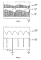
- Fig. 2 shows for an embodiment that with the in Fig. 1 has been realized, the time profile of the envelope for the current I LED , the collector-emitter voltage U CE of the Buck main switch Q1 and the frequency modulation.
- the minimum frequency is 23.12 kHz, the maximum frequency is 28.16 kHz.
- the Buck main switch Q1 is operated in Critical Conduction Mode, the current I LED never drops to zero due to the effect of the capacitors C2 and C3. Its minimum in the present case is about 60 mA, its maximum 130 mA.
- Fig. 3 20 ⁇ s per time unit. It shows the time course of the current I LED and the collector-emitter voltage U ce of the Buck main switch Q1. As can be clearly recognized from the time course of the voltage U ce is, the on time t on of the Buck main switch Q1 is about 2 microseconds, while the off time t off is about 38 microseconds.
- the ground triangular shape of the time profile of the current I LED is due to the effect of the capacitors C2 and C3.
Landscapes
- Engineering & Computer Science (AREA)
- Power Engineering (AREA)
- Dc-Dc Converters (AREA)
- Circuit Arrangement For Electric Light Sources In General (AREA)
Description
- Die vorliegende Erfindung betrifft einen Buck-Konverter zum Bereitstellen eines Stroms für mindestens eine LED mit einem Eingang mit einem ersten und einem zweiten Eingangsanschluss zum Anschließen einer Gleichspannungsquelle, einem Ausgang mit einem ersten und einem zweiten Ausgangsanschluss zum Anschließen der mindestens einen LED, und einer Buckdiode, einer Buckdrossel und einem Buck-Hauptschalter, der eine Steuerelektrode, eine Arbeitselektrode und eine Bezugselektrode aufweist.
- Mit dem Vordringen von LEDs in weite Bereiche der Allgemeinbeleuchtung ergibt sich ein großer Bedarf an einfachen und kostengünstigen Stromversorgungsschaltungen für diese Bauteile. Eine für Netzanwendungen zum Betrieb von LEDs bekannte Wandlerschaltung ist der so genannte Sperrwandler, für den auch der Name Flyback gebräuchlich ist. Weiterhin gibt es mittlerweile eine Vielzahl von insbesondere integrierten Schaltungen für Buck- oder Boost-Konverter, zum Beispiel das Steuer-IC MXHV9910 von der Firma Micronix. Der Nachteil an diesen Realisierungen besteht darin, dass sie alle einen recht erheblichen Aufwand benötigen und auf die Verwendung teurer Bauteile angewiesen sind. So muss der Schalter eines Sperrwandlers bei europäischer Netzspannung eine Spannungsfestigkeit von mindestens 700 V aufweisen. Für den Einsatz in Massenprodukten übersteigen die dadurch entstehenden Kosten häufig das vorgegebenen Budget.
- Die Aufgabe der vorliegenden Erfindung besteht deshalb darin, einen eingangs genannten Buck-Konverter derart weiterzubilden, dass er äußerst preisgünstig realisiert werden kann.
- Diese Aufgabe wird gelöst durch einen Buck-Konverter mit den Merkmalen von Patentanspruch 1.
- Der vorliegenden Erfindung liegt die Erkenntnis zugrunde, dass sehr preisgünstige Bipolartransistoren, wie sie beispielsweise der aus dem Videobereich bekannte Typ MPSA42 darstellen, bei den für eine Leistungs-LED notwendigen Strömen zum einen nur noch eine geringe Stromverstärkung haben, zum anderen aber zu einem definierten Zeitpunkt abgeschaltet werden müssen, damit sich für die LED ebenfalls ein definierter Strom einstellt.
- Die Erfindung basiert nun weiterhin darauf, dass zur Reduktion der Belastung des Schalters die Buckdiode und der Buck-Hauptschalter seriell zwischen den ersten und den zweiten Eingangsanschluss gekoppelt sind, wobei der Verbindungspunkt zwischen der Buckdiode und dem Buck-Hauptschalter mit dem zweiten Ausgangsanschluss gekoppelt ist. Der erste Anschluss der Buckdrossel ist mit dem ersten Eingangsanschluss und der zweite Anschluss der Buckdrossel mit dem ersten Ausgangsanschluss gekoppelt. Das Problem der geringen Stromverstärkung im Bereich der Ströme, die zum Betrieb von Leistungs-LEDs nötig sind, wird erfindungsgemäß dadurch gelöst, dass eine Maßnahme getroffen wurde, um ausreichend Basisstrom für den Buck-Hauptschalter bereitzustellen. Dazu umfasst der Buck-Konverter weiterhin eine erste mit der Buckdrossel gekoppelte Hilfswicklung, die einen ersten Anschluss aufweist, der mit dem zweiten Eingangsanschluss gekoppelt ist, und einen zweiten Anschluss, der mit der Steuerelektrode des Buck-Hauptschalters gekoppelt ist, wobei die erste Hilfswicklung derart mit der Buckdrossel gekoppelt ist, dass bei einem Stromfluss durch den Buck-Hauptschalter durch die erste Hilfswicklung ein Strom an die Steuerelektrode des Buck-Hauptschalters bereitgestellt wird.
- Diese Maßnahmen ermöglichen die Realisierung eines äußerst einfachen und kostengünstigen Aufbaus eines Buck-Konverters. Sie ermöglichen überdies einen Betrieb im Critical Conduction Mode, bei dem praktisch nur Abschaltverluste für den Buck-Hauptschalter auftreten.
- Bei einer bevorzugten Ausführungsform umfasst der Buck-Konverter weiterhin einen Strommesswiderstand, der seriell zum Buck-Hauptschalter, insbesondere zwischen den von der Buckdiode und dem Buck-Hauptschalter definierten Verbindungspunkt und den zweiten Eingangsanschluss, gekoppelt ist sowie einen ersten Hilfsschalter zum Ausschalten des Buck-Hauptschalters, wobei der erste Hilfsschalter eine Steuerelektrode, eine Arbeitselektrode und eine Bezugselektrode aufweist, wobei die Bezugselektrode des ersten Hilfsschalters mit dem zweiten Eingangsanschluss gekoppelt ist und wobei die Steuerelektrode des ersten Hilfsschalters mit dem Strommesswiderstand gekoppelt ist. Durch diese Anordnung wird bei Erreichen eines vorgebbaren Maximalstroms durch den Buck-Hauptschalter am Strommesswiderstand eine Spannung erzeugt, die zum Einschalten des ersten Hilfsschalters führt, wobei das Einschalten des ersten Hilfsschalters den Buck-Hauptschalter ausschaltet.
- Bevorzugt umfasst der Buck-Konverter weiterhin ein Zeitglied, das zwischen den Strommesswiderstand und die Steuerelektrode des ersten Hilfsschalters gekoppelt ist. Dadurch kann sichergestellt werden, dass der erste Hilfsschalter eingeschaltet bleibt, obwohl der an seiner Steuerelektrode bereitgestellte Strom aufgrund des Ausschaltens des Buck-Hauptschalters schon sinkt. Eine bevorzugte Zeitkonstante liegt beispielsweise in der Größenordnung zwischen 0,2 und 10 µs, bevorzugt 1 µs.
- Weiterhin bevorzugt ist zwischen den zweiten Anschluss der ersten Hilfswicklung und der Steuerelektrode des Buck-Hauptschalters ein erster ohmscher Widerstand gekoppelt. Weiterhin bevorzugt ist dabei der Verbindungspunkt zwischen dem ersten ohmschen Widerstand und der Steuerelektrode des Buck-Hauptschalters über einen zweiten ohmschen Widerstand mit dem zweiten Eingangsanschluss gekoppelt. Damit wird die Steuerstrecke des Buck-Hauptschalters relativ niederohmig abgeschlossen und ist damit gegenüber eingekoppelten Störungen unempfindlich.
- Weiterhin bevorzugt ist die Steuerelektrode des Buck-Hauptschalters mit der Arbeitselektrode des ersten Hilfsschalters gekoppelt.
- Bei einer bevorzugten Weiterbildung kann vorgesehen sein, dass der Buck-Konverter weiterhin einen zweiten Hilfsschalter zum Starten des Buck-Konverters umfasst, wobei der zweite Hilfsschalter eine Steuerelektrode, eine Arbeitselektrode und eine Bezugselektrode aufweist, wobei die Bezugselektrode des zweiten Hilfsschalters mit dem ersten Eingangsanschluss gekoppelt ist, wobei die Steuerelektrode des zweiten Hilfsschalters über einen ohmschen Widerstand mit dem zweiten Eingangsanschluss gekoppelt ist. Durch diese Maßnahme wird sichergestellt, dass der zweite Hilfsschalter einschaltet, sobald eine Gleichspannungsquelle zwischen dem ersten und dem zweiten Eingangsanschluss angeschlossen wird.
- Bevorzugt ist die Arbeitselektrode des zweiten Hilfsschalters über einen ohmschen Widerstand mit der Arbeitselektrode des ersten Hilfsschalters gekoppelt. Sobald der zweite Hilfsschalter eingeschaltet ist, wird dann über diesen ohmschen Widerstand ein Strom an die Steuerelektrode des Buck-Hauptschalters bereitgestellt, so dass dieser ebenfalls einschaltet. In die Steuerelektrode des Buck-Hauptschalters fließen demnach der durch die erste Hilfswicklung erzeugte Strom sowie der über den eingeschalteten zweiten Hilfsschalter fließende Strom.
- Bevorzugt umfasst der Buck-Konverter weiterhin eine zweite, mit der Buckdrossel gekoppelte Hilfswicklung, die einen ersten Anschluss aufweist, der mit dem ersten Eingangsanschluss gekoppelt ist, und einen zweiten Anschluss, der mit der Steuerelektrode des zweiten Hilfsschalters gekoppelt ist. Bevorzugt ist dabei zwischen den zweiten Anschluss der zweiten Hilfswicklung und der Steuerelektrode des zweiten Hilfsschalters ein ohmscher Widerstand gekoppelt, vorzugsweise die Serienschaltung eines ohmschen Widerstands und einer Diode. Dabei ist die zweite Hilfswicklung insbesondere derart mit der Buckdrossel gekoppelt, dass während der Sperrphase des Buck-Hauptschalters bzw. der Entmagnetisierungsphase der Buckdrossel ein Strom an die Steuerelektrode des zweiten Hilfsschalters derart bereitgestellt wird, dass der zweite Hilfsschalter gesperrt wird. Dadurch kann ein Stromfluss durch den ohmschen Widerstand, der die Arbeitselektrode des zweiten Hilfsschalters mit der Arbeitselektrode des ersten Hilfsschalters koppelt, verhindert werden, so dass in diesem ohmschen Widerstand nur in den kurzen Einschaltphasen des Buck-Hauptschalters Verlustleistung entsteht und dieser in den langen Ausschaltphasen des Buck-Hauptschalters quasi verlustfrei betrieben wird.
- Zur Reduktion der Welligkeit (Rippel) des an die mindestens eine LED bereitgestellten Stroms ist weiterhin bevorzugt zwischen den ersten und den zweiten Ausgangsanschluss mindestens ein Kondensator gekoppelt.
- Weitere bevorzugte Ausführungsformen ergeben sich aus den Unteransprüchen.
- Im Nachfolgenden wird nunmehr ein Ausführungsbeispiel eines erfindungsgemäßen Buck-Konverters unter Bezugnahme auf die beigefügten Zeichnungen näher beschrieben. Es zeigen:
- Fig. 1
- in schematischer Darstellung ein Ausführungsbei- spiel eines erfindungsgemäßen Buck-Konverters;
- Fig. 2
- den zeitlichen Verlauf der Kollektor-Emitter- Spannung am Buck-Hauptschalter sowie des an die mindestens eine LED bereitgestellten Stroms ILED in einer ersten zeitlichen Auflösung; und
- Fig. 3
- den zeitlichen Verlauf der Kollektor-Emitter- Spannung am Buck-Hauptschalter sowie des an die mindestens eine LED bereitgestellten Stroms ILED in einer zweiten zeitlichen Auflösung.
-
Fig. 1 zeigt in schematischer Darstellung ein Ausführungsbeispiel eines erfindungsgemäßen Buck-Konverters. Dieser weist einen ersten E1 und einen zweiten Eingangsanschluss E2 auf, die über einen Gleichrichter GL1 mit Netzanschlüssen L, N verbunden sind. Eine zwischen dem Netzanschluss L und dem Gleichrichter GL1 angeordnete Induktivität L1 dient der Einschaltstrombegrenzung und der Funkentstörung. Zur Pufferung der gleichgerichteten Netzspannung ist ein Kondensator C9 vorgesehen. Zwischen die Eingangsanschlüsse E1 und E2 ist in üblicher Weise eine Serienschaltung einer Buckdiode D2 sowie eines Buck-Hauptschalters Q1 gekoppelt. Eine Buckdrossel ist zwischen den ersten Eingangsanschluss E1 und einen ersten Ausgangsanschluss A1 gekoppelt, wobei vorliegend die Buckdrossel als erste Wicklung w1 eines Transformators TR1 ausgeführt ist, der überdies eine erste w2 und eine zweite w3 Hilfswicklung trägt. Der zwischen der Buckdiode D2 und dem Buck-Hauptschalter Q1 angeordnete Verbindungspunkt VP1 ist mit dem zweiten Ausgangsanschluss A2 des Buck-Konverters gekoppelt. Zwischen die Ausgangsanschlüsse A1, A2 sind zwei Kondensatoren C2, C3 gekoppelt. - Zwischen den Emitter des Buck-Hauptschalters Q1 und den zweiten Eingangsanschluss E2 ist als Shunt ein ohmscher Widerstand R6 angeordnet. Die an diesem Widerstand R6 abfallende Spannung wird über ein Zeitglied, das den ohmschen Widerstand R3 sowie den Kondensator C1 umfasst, über einen ohmschen Widerstand R4 an die Basis eines ersten Hilfsschalters Q3 geführt, da der Strom durch den Buck-Hauptschalter Q1 nach dessen Ausschalten in ungefähr 200 bis 300 ns auf Null sinkt. Durch dieses Zeitglied kann sichergestellt werden, dass der erste Hilfsschalter Q3 länger eingeschaltet bleibt, als dies bei einer direkten Kopplung, d.h. ohne Zwischenschaltung eines Zeitglieds, der am Widerstand R6 abfallenden Spannung an die Basis des ersten Hilfsschalters Q3 der Fall wäre.
- Die Steuerelektrode des Buck-Hauptschalters Q1 ist erstens über einen Widerstand R1 mit der Hilfswicklung w3 gekoppelt, zweitens mit der Arbeitselektrode des Hilfsschalters Q3. Überdies ist die Steuerelektrode des Buck-Hauptschalters Q1 drittens über einen ohmschen Widerstand R2 mit dem zweiten Eingangsanschluss E2 gekoppelt. Ein weiterer Hilfsschalter Q2 ist mit seiner Bezugselektrode mit dem ersten Eingangsanschluss E1 gekoppelt und mit seiner Arbeitselektrode über einen ohmschen Widerstand R8 mit der Arbeitselektrode des Hilfsschalters Q3. Die Steuerelektrode des Hilfsschalters Q2 ist einerseits über einen ohmschen Widerstand R5 mit dem zweiten Eingangsanschluss E2 gekoppelt, andererseits über die Serienschaltung einer Diode D1 und eines ohmschen Widerstands R7 mit der Hilfswicklung w2. Die Diode D1 wirkt hier als Anlaufdiode bei zu kleiner Netzspannung, d. h. der Schalter Q2 wird erst eingeschaltet ab einer Netzspannung von 160 bis 170 V.
- Während die Hilfswicklung w3 gleichsinnig mit der Wicklung w1 gewickelt ist, ist der Wicklungssinn der Wicklung w2 zum Wicklungssinn der Wicklung w1 gegensinnig.
- Zur Funktionsweise: Nach dem Anlegen einer Netzspannung fließt ein Strom über den Eingangsanschluss E2, die Hilfswicklung w2, den ohmschen Widerstand R7, die Diode D1 und den ohmschen Widerstand R5 und führt zum Einschalten des Hilfstransistors Q2. Dadurch wird ein Basisstrom an die Basis des Buck-Hauptschalters Q1 bereitgestellt, was zum Einschalten des Buck-Hauptschalters Q1 führt. Dabei ist durch geeignete Dimensionierung des Transformators TR1, insbesondere geeignete Auslegung der Wicklung w3, sichergestellt, dass der Buck-Hauptschalter Q1 selbst bei hohen, an die mindestens eine LED bereitgestellten Strömen mit einem ausreichenden Basisstrom versorgt wird. Durch die Hilfswicklung w3 wird genau dann ein Basisstrom für den Buck-Hauptschalter Q1 zur Verfügung gestellt, wenn dieser benötigt wird, und zwar wenn der Buck-Hauptschalter Q1 eingeschaltet ist. Erzeugt der Emitterstrom des Buck-Hauptschalters einen Spannungsabfall am Shunt R6, der ausreicht, den Hilfsschalter Q3 einzuschalten, fließt der vom Hilfsschalter Q2 bereitgestellte Strom nicht mehr an die Steuerelektrode des Buck-Hauptschalters Q1, sondern über den Hilfsschalter Q3 zum Eingangsanschluss E2. Dadurch wird der Buck-Hauptschalter Q1 abgeschaltet.
- Im Gegensatz zu einem Sperrwandler wird vorliegend der Buck-Hauptschalter Q1 maximal mit der zwischen den Eingangsanschlüssen E1, E2 anliegenden Spannung belastet. Die Schaltung ist üblicherweise so dimensioniert, dass die Ausschaltzeit toff ungefähr das 20-fache der Anschaltzeit ton beträgt. In einem bevorzugten Ausführungsbeispiel beträgt die Ausschaltzeit toff ca. 40 µs und die Anschaltzeit ton entsprechend 2 µs.
- Durch die Rückkopplungswicklungen w2 und w3 wird demnach sichergestellt, dass der Buck-Hauptschalter Q1 und der Hilfsschalter Q2 sicher gesperrt sind, bis die Buckdrossel TR1, w1 vollständig entmagnetisiert ist. Dadurch wird der Buck-Hauptschalter Q1 im Critical Conduction Mode (Transition Mode) betrieben, so dass er in der nächsten Periode verlustarm einschalten kann, d. h. der den Buck-Hauptschalter Q1 durchfließende Strom ist zum Einschaltzeitpunkt nahezu Null. Die Frequenz des dreieckförmigen Stroms durch die Buckdrossel TR1, w1 wird durch die zwischen den Anschlüssen anliegende Eingangsnetzspannung UN, die am Ausgang anliegende LED-Spannung ULED, die Induktivität der Buckdrossel TR1, w1 und den Grenzwert für den maximalen LED-Strom ILED festgelegt.
-
Fig. 2 zeigt für ein Ausführungsbeispiel, das mit den inFig. 1 angegebenen Dimensionierungen realisiert wurde, den zeitlichen Verlauf der Hüllkurve für den Strom ILED, die Kollektor-Emitter-Spannung UCE des Buck-Hauptschalters Q1 sowie die Frequenzmodulation. Die minimale Frequenz beträgt 23,12 kHz, die maximale Frequenz 28,16 kHz. Trotz dessen, dass der Buck-Hauptschalter Q1 im Critical Conduction Mode betrieben wird, sinkt der Strom ILED aufgrund der Wirkung der Kondensatoren C2 und C3 nie auf Null. Sein Minimum beträgt vorliegend ca. 60 mA, sein Maximum 130 mA. - Während die Aufzeichnung von
Fig. 2 mit einer Auflösung von 2 ms pro Zeiteinheit (= Kästchen) gemacht wurde, beträgt die Auflösung inFig. 3 20 µs pro Zeiteinheit. Sie zeigt den zeitlichen Verlauf des Stroms ILED und der Kollektor-Emitter-Spannung Uce des Buck-Hauptschalters Q1. Wie an dem zeitlichen Verlauf der Spannung Uce gut zu erkennen ist, beträgt die Einschaltzeit ton des Buck-Hauptschalters Q1 etwa 2 µs, während die Ausschaltzeit toff ca. 38 µs beträgt. Die verschliffene Dreieckform des zeitlichen Verlaufs des Stroms ILED ergibt sich aufgrund der Wirkung der Kondensatoren C2 und C3.
Claims (12)
- Buck-Konverter zum Bereitstellen eines Stroms für mindestens eine LED mit- einem Eingang mit einem ersten (E1) und einem zweiten Eingangsanschluss (E2) zum Anschließen einer Gleichspannungsquelle;- einem Ausgang mit einem ersten (A1) und einem zweiten Ausgangsanschluss (A2) zum Anschließen der mindestens einen LED; und- einer Buckdiode (D2), einer Buckdrossel (TR1, w1) und einem Buck-Hauptschalter (Q1), der eine Steuerelektrode, eine Arbeitselektrode und eine Bezugselektrode aufweist;wobei die Buckdiode (D2) und der Buck-Hauptschalter (Q1) seriell zwischen den ersten (E1) und den zweiten Eingangsanschluss (E2) gekoppelt sind;
wobei der erste Anschluss der Buckdrossel (TR1, w1) mit dem ersten Eingangsanschluss (E1) gekoppelt ist;
wobei der Buck-Konverter weiterhin umfasst:eine erste mit der Buckdrossel (TR1, w1) gekoppelte Hilfswicklung (TR1, w3), die einen ersten Anschluss aufweist, der mit dem zweiten Eingangsanschluss (E2) gekoppelt ist, und einen zweiten Anschluss, der mit der Steuerelektrode des Buck-Hauptschalters (Q1) gekoppelt ist, wobei die erste Hilfswicklung (TR1, w3) derart mit der Buckdrossel (TR1, w1) gekoppelt ist, dass bei einem Stromfluss durch den Buck-Hauptschalter (Q1) durch die erste Hilfswicklung (TR1, w3) ein Strom an die Steuerelektrode des Buck-Hauptschalters (Q1) bereitgestellt wird ,
dadurch gekennzeichnet, der Verbindungspunkt (VP1) zwischen der Buckdiode (D2) und dem Buck-Hauptschalter (Q1) mit dem zweiten Ausgangsanschluss (A2) gekoppelt ist;
der zweite Anschluss der Buckdrossel (TR1, w1) mit dem ersten Ausgangsanschluss (A1) gekoppelt ist. - Buck-Konverter nach Anspruch 1,
dadurch gekennzeichnet,
dass der Buck-Konverter weiterhin umfasst:einen Strommesswiderstand (R6), der seriell zum Buck-Hauptschalter (Q1), insbesondere zwischen den von der Buckdiode (D2) und dem Buck-Hauptschalter (Q1) definierten Verbindungspunkt (VP1) und den zweiten Eingangsanschluss (E2), gekoppelt ist, sowie einen ersten Hilfsschalter (Q3) zum Ausschalten des Buck-Hauptschalters (Q1), wobei der erste Hilfsschalter (Q3) eine Steuerelektrode, eine Arbeitselektrode und eine Bezugselektrode aufweist, wobei die Bezugselektrode des ersten Hilfsschalters (Q3) mit dem zweiten Eingangsanschluss (E2) gekoppelt ist und wobei die Steuerelektrode des ersten Hilfsschalters (Q3) mit dem Strommesswiderstand (R6) gekoppelt ist. - Buck-Konverter nach Anspruch 2,
dadurch gekennzeichnet,
dass der Buck-Konverter weiterhin ein Zeitglied (C1, R3) umfasst, das zwischen den Strommesswiderstand und die Steuerelektrode des ersten Hilfsschalters (Q3) gekoppelt ist. - Buck-Konverter nach einem der vorhergehenden Ansprüche,
dadurch gekennzeichnet,
dass zwischen den zweiten Anschluss der ersten Hilfswicklung (TR1, w3) und der Steuerelektrode des Buck-Hauptschalters (Q1) ein erster ohmscher Widerstand (R1) gekoppelt ist. - Buck-Konverter nach Anspruch 4,
dadurch gekennzeichnet,
dass der Verbindungspunkt zwischen dem ersten ohmschen Widerstand (R1) und der Steuerelektrode des Buck-Hauptschalters (Q1) über einen zweiten ohmschen Widerstand (R2) mit dem zweiten Eingangsanschluss (E2) gekoppelt ist. - Buck-Konverter nach einem der Ansprüche 2 bis 5,
dadurch gekennzeichnet,
dass die Steuerelektrode des Buck-Hauptschalters (Q1) mit der Arbeitselektrode des ersten Hilfsschalters (Q3) gekoppelt ist. - Buck-Konverter nach einem der vorhergehenden Ansprüche,
dadurch gekennzeichnet,
dass der Buck-Konverter weiterhin umfasst:einen zweiten Hilfsschalter (Q2) zum Starten des Buck-Konverters, wobei der zweite Hilfsschalter (Q2) eine Steuerelektrode, eine Arbeitselektrode und eine Bezugselektrode aufweist, wobei die Bezugselektrode des zweiten Hilfsschalters (Q2) mit dem ersten Eingangsanschluss (E1) gekoppelt ist, wobei die Steuerelektrode des zweiten Hilfsschalters (Q2) über einen ohmschen Widerstand (R5) mit dem zweiten Eingangsanschluss (E2) gekoppelt ist. - Buck-Konverter nach Anspruch 7,
dadurch gekennzeichnet,
dass die Arbeitselektrode des zweiten Hilfsschalters (Q2) über einen ohmschen Widerstand (R8) mit der Arbeitselektrode des ersten Hilfsschalters (Q3) gekoppelt ist. - Buck-Konverter nach einem der vorhergehenden Ansprüche,
dadurch gekennzeichnet,
dass der Buck-Konverter weiterhin umfasst:eine zweite mit der Buckdrossel gekoppelte Hilfswicklung (TR1, w2), die einen ersten Anschluss aufweist, der mit dem ersten Eingangsanschluss (E1) gekoppelt ist, und einen zweiten Anschluss, der mit der Steuerelektrode des zweiten Hilfsschalters (Q2) gekoppelt ist. - Buck-Konverter nach Anspruch 9,
dadurch gekennzeichnet,
dass zwischen den zweiten Anschluss der zweiten Hilfswicklung (TR1, w2) und der Steuerelektrode des zweiten Hilfsschalters (Q2) ein ohmscher Widerstand (R7) gekoppelt ist, vorzugsweise die Serienschaltung eines ohmschen Widerstands (R7) und einer Diode (D1). - Buck-Konverter nach einem Ansprüche 9 oder 10,
dadurch gekennzeichnet,
dass die zweite Hilfswicklung (TR1, w2) derart mit der Buckdrossel (TR1, w1) gekoppelt ist, dass während der Entmagnetisierungsphase der Buckdrossel (TR1, w1) ein Strom an die Steuerelektrode des zweiten Hilfsschalters (Q2) derart bereitgestellt wird, dass der zweite Hilfsschalter (Q2) gesperrt wird. - Buck-Konverter nach einem der vorhergehenden Ansprüche,
dadurch gekennzeichnet,
dass zwischen den ersten (A1) und den zweiten Ausgangsanschluss (A2) mindestens ein Kondensator (C2; C3) gekoppelt ist.
Applications Claiming Priority (1)
| Application Number | Priority Date | Filing Date | Title |
|---|---|---|---|
| PCT/EP2008/050581 WO2009089919A1 (de) | 2008-01-18 | 2008-01-18 | Buck-konverter zum bereitstellen eines stroms für mindestens eine led |
Publications (2)
| Publication Number | Publication Date |
|---|---|
| EP2232686A1 EP2232686A1 (de) | 2010-09-29 |
| EP2232686B1 true EP2232686B1 (de) | 2011-07-20 |
Family
ID=39760445
Family Applications (1)
| Application Number | Title | Priority Date | Filing Date |
|---|---|---|---|
| EP08701587A Not-in-force EP2232686B1 (de) | 2008-01-18 | 2008-01-18 | Buck-konverter zum bereitstellen eines stroms für mindestens eine led |
Country Status (8)
| Country | Link |
|---|---|
| US (1) | US8207683B2 (de) |
| EP (1) | EP2232686B1 (de) |
| JP (1) | JP5216103B2 (de) |
| KR (1) | KR101480687B1 (de) |
| CN (1) | CN101919146B (de) |
| AT (1) | ATE517461T1 (de) |
| TW (1) | TWI471065B (de) |
| WO (1) | WO2009089919A1 (de) |
Families Citing this family (14)
| Publication number | Priority date | Publication date | Assignee | Title |
|---|---|---|---|---|
| DE102009042433B4 (de) * | 2009-09-22 | 2011-09-15 | Osram Gesellschaft mit beschränkter Haftung | Schaltungsanordnung zum Betreiben mindestens einer LED |
| CN102076148A (zh) | 2009-11-09 | 2011-05-25 | 东芝照明技术株式会社 | Led点灯装置以及照明装置 |
| BRPI1000249A2 (pt) * | 2010-01-27 | 2011-09-20 | Whirlpool Sa | fonte de alimentação de baixa tensão |
| EP2364062A3 (de) | 2010-01-27 | 2013-04-10 | Toshiba Lighting & Technology Corporation | LED-Lichtvorrichtung und Beleuchtungsvorrichtung |
| JP2011155101A (ja) * | 2010-01-27 | 2011-08-11 | Toshiba Lighting & Technology Corp | Led点灯装置 |
| JP5633789B2 (ja) | 2010-05-14 | 2014-12-03 | 東芝ライテック株式会社 | 直流電源装置およびled照明装置 |
| DE102010031669B4 (de) * | 2010-07-22 | 2014-10-09 | Osram Gmbh | Buck-Konverter und Verfahren zum Bereitstellen eines Stroms für mindestens eine LED |
| CH704071A1 (de) * | 2010-11-15 | 2012-05-15 | Permotors Gmbh | Schaltungsanordnung zum Betreiben einer elektrischen Last mit gepulster Spannung. |
| SI2489808T1 (sl) | 2011-02-15 | 2014-01-31 | F.J. Aschwanden Ag | Armirni element za prestrezanje sil v betonskih elementih, oprtih na oporne elemente |
| EP2528216B1 (de) | 2011-05-24 | 2017-03-01 | OSRAM GmbH | Selbstschwingender Abwärtswandler |
| JP5863282B2 (ja) * | 2011-06-03 | 2016-02-16 | ローム株式会社 | Ledランプ、電源モジュール、トランス回路 |
| EP2814159B1 (de) * | 2012-02-09 | 2017-06-28 | Panasonic Intellectual Property Management Co., Ltd. | Stromversorgungsschaltung |
| TWI678948B (zh) | 2018-06-12 | 2019-12-01 | 義守大學 | 照明系統及其驅動電路 |
| US20230327404A1 (en) * | 2022-04-11 | 2023-10-12 | Cisco Technology, Inc. | Inverted slab-coupled optical waveguide |
Family Cites Families (13)
| Publication number | Priority date | Publication date | Assignee | Title |
|---|---|---|---|---|
| US3500127A (en) * | 1967-11-28 | 1970-03-10 | Rca Corp | Switching type voltage and current regulator and load therefor |
| JPS5915438Y2 (ja) * | 1978-07-14 | 1984-05-08 | 池田電機株式会社 | 水銀灯点灯装置 |
| US4823023A (en) * | 1982-06-01 | 1989-04-18 | Nippon Chemi-Con Corporation | Transistor with differentiated control switching circuit |
| JPS6334896A (ja) * | 1986-07-28 | 1988-02-15 | 松下電工株式会社 | 放電灯点灯装置 |
| TW349287B (en) * | 1996-09-12 | 1999-01-01 | Thomson Consumer Electronics | A forward converter with an inductor coupled to a transformer winding |
| US7071762B2 (en) * | 2001-01-31 | 2006-07-04 | Koninklijke Philips Electronics N.V. | Supply assembly for a led lighting module |
| JP2005051942A (ja) * | 2003-07-30 | 2005-02-24 | Noritz Corp | スイッチング電源回路およびこれを備えたスイッチングレギュレータ |
| JP2007073781A (ja) * | 2005-09-08 | 2007-03-22 | Matsushita Electric Ind Co Ltd | 発光ダイオード駆動装置 |
| EP1858301A1 (de) * | 2006-05-16 | 2007-11-21 | Patent-Treuhand-Gesellschaft für elektrische Glühlampen mbH | LED-Beleuchtungssystem und -verfahren zur Erzeugung einer vorgebbaren Farbsequenz |
| EP1868284B1 (de) * | 2006-06-15 | 2013-07-24 | OSRAM GmbH | LED Ansteuerschaltung |
| KR20090087048A (ko) * | 2006-11-09 | 2009-08-14 | 오스람 게젤샤프트 미트 베쉬랭크터 하프퉁 | 자기-발진 dc-dc 컨버터 및 방법 |
| EP2092802A1 (de) * | 2006-11-22 | 2009-08-26 | Osram Gesellschaft mit Beschränkter Haftung | Schaltungsanordnung und verfahren zum betreiben einer entladungslampe mit vorheizbaren elektroden |
| CN102055357B (zh) * | 2009-10-27 | 2013-01-09 | 聚辰半导体(上海)有限公司 | 开关电源控制器电路及开关电源系统 |
-
2008
- 2008-01-18 CN CN2008801250793A patent/CN101919146B/zh not_active Expired - Fee Related
- 2008-01-18 JP JP2010542537A patent/JP5216103B2/ja not_active Expired - Fee Related
- 2008-01-18 KR KR1020107018248A patent/KR101480687B1/ko not_active Expired - Fee Related
- 2008-01-18 WO PCT/EP2008/050581 patent/WO2009089919A1/de not_active Ceased
- 2008-01-18 EP EP08701587A patent/EP2232686B1/de not_active Not-in-force
- 2008-01-18 AT AT08701587T patent/ATE517461T1/de active
- 2008-01-18 US US12/812,960 patent/US8207683B2/en not_active Expired - Fee Related
- 2008-12-31 TW TW97151603A patent/TWI471065B/zh not_active IP Right Cessation
Also Published As
| Publication number | Publication date |
|---|---|
| US8207683B2 (en) | 2012-06-26 |
| CN101919146B (zh) | 2013-07-31 |
| CN101919146A (zh) | 2010-12-15 |
| KR101480687B1 (ko) | 2015-01-21 |
| JP5216103B2 (ja) | 2013-06-19 |
| EP2232686A1 (de) | 2010-09-29 |
| JP2011510604A (ja) | 2011-03-31 |
| TW200935979A (en) | 2009-08-16 |
| WO2009089919A1 (de) | 2009-07-23 |
| ATE517461T1 (de) | 2011-08-15 |
| US20110050129A1 (en) | 2011-03-03 |
| TWI471065B (zh) | 2015-01-21 |
| KR20100103701A (ko) | 2010-09-27 |
Similar Documents
| Publication | Publication Date | Title |
|---|---|---|
| EP2232686B1 (de) | Buck-konverter zum bereitstellen eines stroms für mindestens eine led | |
| DE102013002266B4 (de) | Bootstrap-Schaltungsanordnung für einen IGBT | |
| DE19548506A1 (de) | Schaltungsanordnung zum Betrieb einer Lampe | |
| DE60313733T2 (de) | Ansteuerschaltung für einen Steueranschluss eines Bipolartransistors, der in der Emitterschattkonfiguration ist und entsprechenes Ansteuerverfahren | |
| DE69413798T2 (de) | Elektronische Leistungsvorrichtung mit drei Anschlüssen und isoliertem Gate mit einer Sättigungsausgangskennlinie veränderlicher Neigung in diskontinuierlicher Abhängigkeit vom Ausgangsstrom | |
| EP2446526B1 (de) | Schaltungsanordnung zum betreiben mindestens einer led | |
| EP0287166B1 (de) | Schaltungsanordnung zur Begrenzung der Einschaltstromspitzen bei einem Schalttransistor | |
| DE4413546A1 (de) | Gleichstrom-Steuerschaltung | |
| DE3813672A1 (de) | Wechselrichter fuer eine induktive last | |
| DE4429733A1 (de) | Leistungsschaltvorrichtung | |
| DE19602121C1 (de) | Strombegrenzungsschaltung | |
| DE3504803A1 (de) | Gegentaktgenerator | |
| EP1195885B1 (de) | Synchrongleichrichterschaltung | |
| DE102018122061A1 (de) | Leitungswandlungsvorrichtung | |
| EP2140735B1 (de) | Schaltungsanordnung zum zünden und betreiben mindestens einer entladungslampe | |
| EP0757420B1 (de) | Elektronisches Vorschaltgerät mit Einschaltstrombegrenzung und/oder Überspannungsschutz | |
| DE3411912C2 (de) | ||
| DE102010022380A1 (de) | Schaltreglerschaltung und Verfahren zur Bereitstellung einer geregelten Spannung | |
| EP1484947B1 (de) | Ansteuerschaltung für den Betrieb mindestens einer Lampe in einem dazugehörigen Lastkreis | |
| EP2690927B1 (de) | Ansteuerschaltung für eine Leuchtmittelanordnung mit einem ansteuerbaren Trennschalter | |
| DE10255357B4 (de) | Gleichspanungswandlerschaltung und Verfahren zur Gleichspannungswandlung | |
| DE69407953T2 (de) | Verbesserter integrierter magnetischer Abwärtskonverter | |
| DE102009035371B4 (de) | Elektronisches Vorschaltgerät zum Betreiben mindestens einer Entladungslampe | |
| DE19730220A1 (de) | Getaktete Stromversorgungsanordnung | |
| DE19702136A1 (de) | Elektronischer Leistungsschalter |
Legal Events
| Date | Code | Title | Description |
|---|---|---|---|
| PUAI | Public reference made under article 153(3) epc to a published international application that has entered the european phase |
Free format text: ORIGINAL CODE: 0009012 |
|
| 17P | Request for examination filed |
Effective date: 20100604 |
|
| AK | Designated contracting states |
Kind code of ref document: A1 Designated state(s): AT BE BG CH CY CZ DE DK EE ES FI FR GB GR HR HU IE IS IT LI LT LU LV MC MT NL NO PL PT RO SE SI SK TR |
|
| AX | Request for extension of the european patent |
Extension state: AL BA MK RS |
|
| GRAP | Despatch of communication of intention to grant a patent |
Free format text: ORIGINAL CODE: EPIDOSNIGR1 |
|
| DAX | Request for extension of the european patent (deleted) | ||
| GRAS | Grant fee paid |
Free format text: ORIGINAL CODE: EPIDOSNIGR3 |
|
| GRAA | (expected) grant |
Free format text: ORIGINAL CODE: 0009210 |
|
| AK | Designated contracting states |
Kind code of ref document: B1 Designated state(s): AT BE BG CH CY CZ DE DK EE ES FI FR GB GR HR HU IE IS IT LI LT LU LV MC MT NL NO PL PT RO SE SI SK TR |
|
| REG | Reference to a national code |
Ref country code: GB Ref legal event code: FG4D Free format text: NOT ENGLISH |
|
| REG | Reference to a national code |
Ref country code: CH Ref legal event code: EP |
|
| REG | Reference to a national code |
Ref country code: DE Ref legal event code: R096 Ref document number: 502008004249 Country of ref document: DE Effective date: 20110915 |
|
| REG | Reference to a national code |
Ref country code: NL Ref legal event code: VDEP Effective date: 20110720 |
|
| PG25 | Lapsed in a contracting state [announced via postgrant information from national office to epo] |
Ref country code: FI Free format text: LAPSE BECAUSE OF FAILURE TO SUBMIT A TRANSLATION OF THE DESCRIPTION OR TO PAY THE FEE WITHIN THE PRESCRIBED TIME-LIMIT Effective date: 20110720 Ref country code: NL Free format text: LAPSE BECAUSE OF FAILURE TO SUBMIT A TRANSLATION OF THE DESCRIPTION OR TO PAY THE FEE WITHIN THE PRESCRIBED TIME-LIMIT Effective date: 20110720 Ref country code: NO Free format text: LAPSE BECAUSE OF FAILURE TO SUBMIT A TRANSLATION OF THE DESCRIPTION OR TO PAY THE FEE WITHIN THE PRESCRIBED TIME-LIMIT Effective date: 20111020 Ref country code: PT Free format text: LAPSE BECAUSE OF FAILURE TO SUBMIT A TRANSLATION OF THE DESCRIPTION OR TO PAY THE FEE WITHIN THE PRESCRIBED TIME-LIMIT Effective date: 20111121 Ref country code: LT Free format text: LAPSE BECAUSE OF FAILURE TO SUBMIT A TRANSLATION OF THE DESCRIPTION OR TO PAY THE FEE WITHIN THE PRESCRIBED TIME-LIMIT Effective date: 20110720 Ref country code: IS Free format text: LAPSE BECAUSE OF FAILURE TO SUBMIT A TRANSLATION OF THE DESCRIPTION OR TO PAY THE FEE WITHIN THE PRESCRIBED TIME-LIMIT Effective date: 20111120 Ref country code: HR Free format text: LAPSE BECAUSE OF FAILURE TO SUBMIT A TRANSLATION OF THE DESCRIPTION OR TO PAY THE FEE WITHIN THE PRESCRIBED TIME-LIMIT Effective date: 20110720 Ref country code: SE Free format text: LAPSE BECAUSE OF FAILURE TO SUBMIT A TRANSLATION OF THE DESCRIPTION OR TO PAY THE FEE WITHIN THE PRESCRIBED TIME-LIMIT Effective date: 20110720 |
|
| REG | Reference to a national code |
Ref country code: DE Ref legal event code: R081 Ref document number: 502008004249 Country of ref document: DE Owner name: OSRAM GMBH, DE Free format text: FORMER OWNER: OSRAM GESELLSCHAFT MIT BESCHRAENKTER HAFTUNG, 81543 MUENCHEN, DE Effective date: 20111214 |
|
| REG | Reference to a national code |
Ref country code: IE Ref legal event code: FD4D |
|
| PG25 | Lapsed in a contracting state [announced via postgrant information from national office to epo] |
Ref country code: CY Free format text: LAPSE BECAUSE OF FAILURE TO SUBMIT A TRANSLATION OF THE DESCRIPTION OR TO PAY THE FEE WITHIN THE PRESCRIBED TIME-LIMIT Effective date: 20110720 Ref country code: GR Free format text: LAPSE BECAUSE OF FAILURE TO SUBMIT A TRANSLATION OF THE DESCRIPTION OR TO PAY THE FEE WITHIN THE PRESCRIBED TIME-LIMIT Effective date: 20111021 Ref country code: LV Free format text: LAPSE BECAUSE OF FAILURE TO SUBMIT A TRANSLATION OF THE DESCRIPTION OR TO PAY THE FEE WITHIN THE PRESCRIBED TIME-LIMIT Effective date: 20110720 Ref country code: SI Free format text: LAPSE BECAUSE OF FAILURE TO SUBMIT A TRANSLATION OF THE DESCRIPTION OR TO PAY THE FEE WITHIN THE PRESCRIBED TIME-LIMIT Effective date: 20110720 Ref country code: PL Free format text: LAPSE BECAUSE OF FAILURE TO SUBMIT A TRANSLATION OF THE DESCRIPTION OR TO PAY THE FEE WITHIN THE PRESCRIBED TIME-LIMIT Effective date: 20110720 |
|
| PG25 | Lapsed in a contracting state [announced via postgrant information from national office to epo] |
Ref country code: SK Free format text: LAPSE BECAUSE OF FAILURE TO SUBMIT A TRANSLATION OF THE DESCRIPTION OR TO PAY THE FEE WITHIN THE PRESCRIBED TIME-LIMIT Effective date: 20110720 Ref country code: IE Free format text: LAPSE BECAUSE OF FAILURE TO SUBMIT A TRANSLATION OF THE DESCRIPTION OR TO PAY THE FEE WITHIN THE PRESCRIBED TIME-LIMIT Effective date: 20110720 Ref country code: CZ Free format text: LAPSE BECAUSE OF FAILURE TO SUBMIT A TRANSLATION OF THE DESCRIPTION OR TO PAY THE FEE WITHIN THE PRESCRIBED TIME-LIMIT Effective date: 20110720 |
|
| PLBE | No opposition filed within time limit |
Free format text: ORIGINAL CODE: 0009261 |
|
| STAA | Information on the status of an ep patent application or granted ep patent |
Free format text: STATUS: NO OPPOSITION FILED WITHIN TIME LIMIT |
|
| PG25 | Lapsed in a contracting state [announced via postgrant information from national office to epo] |
Ref country code: EE Free format text: LAPSE BECAUSE OF FAILURE TO SUBMIT A TRANSLATION OF THE DESCRIPTION OR TO PAY THE FEE WITHIN THE PRESCRIBED TIME-LIMIT Effective date: 20110720 Ref country code: RO Free format text: LAPSE BECAUSE OF FAILURE TO SUBMIT A TRANSLATION OF THE DESCRIPTION OR TO PAY THE FEE WITHIN THE PRESCRIBED TIME-LIMIT Effective date: 20110720 Ref country code: IT Free format text: LAPSE BECAUSE OF FAILURE TO SUBMIT A TRANSLATION OF THE DESCRIPTION OR TO PAY THE FEE WITHIN THE PRESCRIBED TIME-LIMIT Effective date: 20110720 |
|
| 26N | No opposition filed |
Effective date: 20120423 |
|
| PG25 | Lapsed in a contracting state [announced via postgrant information from national office to epo] |
Ref country code: DK Free format text: LAPSE BECAUSE OF FAILURE TO SUBMIT A TRANSLATION OF THE DESCRIPTION OR TO PAY THE FEE WITHIN THE PRESCRIBED TIME-LIMIT Effective date: 20110720 |
|
| BERE | Be: lapsed |
Owner name: OSRAM G.M.B.H. Effective date: 20120131 |
|
| REG | Reference to a national code |
Ref country code: DE Ref legal event code: R097 Ref document number: 502008004249 Country of ref document: DE Effective date: 20120423 |
|
| PG25 | Lapsed in a contracting state [announced via postgrant information from national office to epo] |
Ref country code: MC Free format text: LAPSE BECAUSE OF NON-PAYMENT OF DUE FEES Effective date: 20120131 |
|
| REG | Reference to a national code |
Ref country code: CH Ref legal event code: PL |
|
| PG25 | Lapsed in a contracting state [announced via postgrant information from national office to epo] |
Ref country code: CH Free format text: LAPSE BECAUSE OF NON-PAYMENT OF DUE FEES Effective date: 20120131 Ref country code: LI Free format text: LAPSE BECAUSE OF NON-PAYMENT OF DUE FEES Effective date: 20120131 |
|
| PG25 | Lapsed in a contracting state [announced via postgrant information from national office to epo] |
Ref country code: BE Free format text: LAPSE BECAUSE OF NON-PAYMENT OF DUE FEES Effective date: 20120131 |
|
| REG | Reference to a national code |
Ref country code: DE Ref legal event code: R081 Ref document number: 502008004249 Country of ref document: DE Owner name: OSRAM GMBH, DE Free format text: FORMER OWNER: OSRAM AG, 81543 MUENCHEN, DE Effective date: 20130205 |
|
| PG25 | Lapsed in a contracting state [announced via postgrant information from national office to epo] |
Ref country code: ES Free format text: LAPSE BECAUSE OF FAILURE TO SUBMIT A TRANSLATION OF THE DESCRIPTION OR TO PAY THE FEE WITHIN THE PRESCRIBED TIME-LIMIT Effective date: 20111031 |
|
| PG25 | Lapsed in a contracting state [announced via postgrant information from national office to epo] |
Ref country code: BG Free format text: LAPSE BECAUSE OF FAILURE TO SUBMIT A TRANSLATION OF THE DESCRIPTION OR TO PAY THE FEE WITHIN THE PRESCRIBED TIME-LIMIT Effective date: 20111020 |
|
| PG25 | Lapsed in a contracting state [announced via postgrant information from national office to epo] |
Ref country code: MT Free format text: LAPSE BECAUSE OF FAILURE TO SUBMIT A TRANSLATION OF THE DESCRIPTION OR TO PAY THE FEE WITHIN THE PRESCRIBED TIME-LIMIT Effective date: 20110720 |
|
| REG | Reference to a national code |
Ref country code: DE Ref legal event code: R081 Ref document number: 502008004249 Country of ref document: DE Owner name: OSRAM GMBH, DE Free format text: FORMER OWNER: OSRAM GMBH, 81543 MUENCHEN, DE Effective date: 20130823 |
|
| REG | Reference to a national code |
Ref country code: AT Ref legal event code: MM01 Ref document number: 517461 Country of ref document: AT Kind code of ref document: T Effective date: 20130118 |
|
| PG25 | Lapsed in a contracting state [announced via postgrant information from national office to epo] |
Ref country code: TR Free format text: LAPSE BECAUSE OF FAILURE TO SUBMIT A TRANSLATION OF THE DESCRIPTION OR TO PAY THE FEE WITHIN THE PRESCRIBED TIME-LIMIT Effective date: 20110720 |
|
| PG25 | Lapsed in a contracting state [announced via postgrant information from national office to epo] |
Ref country code: AT Free format text: LAPSE BECAUSE OF NON-PAYMENT OF DUE FEES Effective date: 20130118 Ref country code: LU Free format text: LAPSE BECAUSE OF NON-PAYMENT OF DUE FEES Effective date: 20120118 |
|
| PGFP | Annual fee paid to national office [announced via postgrant information from national office to epo] |
Ref country code: FR Payment date: 20140123 Year of fee payment: 7 |
|
| PGFP | Annual fee paid to national office [announced via postgrant information from national office to epo] |
Ref country code: GB Payment date: 20140121 Year of fee payment: 7 |
|
| PG25 | Lapsed in a contracting state [announced via postgrant information from national office to epo] |
Ref country code: HU Free format text: LAPSE BECAUSE OF FAILURE TO SUBMIT A TRANSLATION OF THE DESCRIPTION OR TO PAY THE FEE WITHIN THE PRESCRIBED TIME-LIMIT Effective date: 20080118 |
|
| GBPC | Gb: european patent ceased through non-payment of renewal fee |
Effective date: 20150118 |
|
| PG25 | Lapsed in a contracting state [announced via postgrant information from national office to epo] |
Ref country code: GB Free format text: LAPSE BECAUSE OF NON-PAYMENT OF DUE FEES Effective date: 20150118 |
|
| REG | Reference to a national code |
Ref country code: FR Ref legal event code: ST Effective date: 20150930 |
|
| PG25 | Lapsed in a contracting state [announced via postgrant information from national office to epo] |
Ref country code: FR Free format text: LAPSE BECAUSE OF NON-PAYMENT OF DUE FEES Effective date: 20150202 |
|
| PGFP | Annual fee paid to national office [announced via postgrant information from national office to epo] |
Ref country code: DE Payment date: 20180122 Year of fee payment: 11 |
|
| REG | Reference to a national code |
Ref country code: DE Ref legal event code: R119 Ref document number: 502008004249 Country of ref document: DE |
|
| PG25 | Lapsed in a contracting state [announced via postgrant information from national office to epo] |
Ref country code: DE Free format text: LAPSE BECAUSE OF NON-PAYMENT OF DUE FEES Effective date: 20190801 |