EP1484928A2 - Bildaufnahmevorrichtung - Google Patents
Bildaufnahmevorrichtung Download PDFInfo
- Publication number
- EP1484928A2 EP1484928A2 EP04013188A EP04013188A EP1484928A2 EP 1484928 A2 EP1484928 A2 EP 1484928A2 EP 04013188 A EP04013188 A EP 04013188A EP 04013188 A EP04013188 A EP 04013188A EP 1484928 A2 EP1484928 A2 EP 1484928A2
- Authority
- EP
- European Patent Office
- Prior art keywords
- pixel
- color component
- imaging device
- component pixel
- color
- Prior art date
- Legal status (The legal status is an assumption and is not a legal conclusion. Google has not performed a legal analysis and makes no representation as to the accuracy of the status listed.)
- Granted
Links
- 238000003384 imaging method Methods 0.000 title claims description 53
- 230000002093 peripheral effect Effects 0.000 claims abstract description 26
- 238000012546 transfer Methods 0.000 claims description 26
- 238000006243 chemical reaction Methods 0.000 claims description 12
- 239000011159 matrix material Substances 0.000 claims description 4
- 230000009193 crawling Effects 0.000 abstract description 10
- 238000009499 grossing Methods 0.000 abstract description 5
- 238000001444 catalytic combustion detection Methods 0.000 description 32
- 238000012545 processing Methods 0.000 description 28
- 238000012937 correction Methods 0.000 description 16
- 230000000875 corresponding effect Effects 0.000 description 16
- 230000006870 function Effects 0.000 description 7
- 230000002596 correlated effect Effects 0.000 description 6
- 230000002708 enhancing effect Effects 0.000 description 6
- 238000012360 testing method Methods 0.000 description 6
- 238000005070 sampling Methods 0.000 description 5
- 238000010586 diagram Methods 0.000 description 4
- 230000000694 effects Effects 0.000 description 4
- 238000000034 method Methods 0.000 description 4
- 238000004364 calculation method Methods 0.000 description 3
- 239000003086 colorant Substances 0.000 description 2
- 230000007547 defect Effects 0.000 description 2
- 230000003287 optical effect Effects 0.000 description 2
- 230000000295 complement effect Effects 0.000 description 1
- 230000006835 compression Effects 0.000 description 1
- 238000007906 compression Methods 0.000 description 1
- 230000001276 controlling effect Effects 0.000 description 1
- 238000010191 image analysis Methods 0.000 description 1
- 238000003706 image smoothing Methods 0.000 description 1
- 230000007774 longterm Effects 0.000 description 1
- 238000004519 manufacturing process Methods 0.000 description 1
- 230000000873 masking effect Effects 0.000 description 1
- 239000000203 mixture Substances 0.000 description 1
- 239000004065 semiconductor Substances 0.000 description 1
- 230000035945 sensitivity Effects 0.000 description 1
- 239000000758 substrate Substances 0.000 description 1
- 239000013589 supplement Substances 0.000 description 1
Images

Classifications
-
- H—ELECTRICITY
- H04—ELECTRIC COMMUNICATION TECHNIQUE
- H04N—PICTORIAL COMMUNICATION, e.g. TELEVISION
- H04N25/00—Circuitry of solid-state image sensors [SSIS]; Control thereof
- H04N25/60—Noise processing, e.g. detecting, correcting, reducing or removing noise
- H04N25/61—Noise processing, e.g. detecting, correcting, reducing or removing noise the noise originating only from the lens unit, e.g. flare, shading, vignetting or "cos4"
- H04N25/611—Correction of chromatic aberration
-
- H—ELECTRICITY
- H04—ELECTRIC COMMUNICATION TECHNIQUE
- H04N—PICTORIAL COMMUNICATION, e.g. TELEVISION
- H04N25/00—Circuitry of solid-state image sensors [SSIS]; Control thereof
- H04N25/10—Circuitry of solid-state image sensors [SSIS]; Control thereof for transforming different wavelengths into image signals
- H04N25/11—Arrangement of colour filter arrays [CFA]; Filter mosaics
- H04N25/13—Arrangement of colour filter arrays [CFA]; Filter mosaics characterised by the spectral characteristics of the filter elements
- H04N25/134—Arrangement of colour filter arrays [CFA]; Filter mosaics characterised by the spectral characteristics of the filter elements based on three different wavelength filter elements
Definitions
- the present invention relates to an imaging device. To be more specific, the present invention relates to image data processing to be performed on an output signal from a color image sensor in order to obtain a high quality image.
- LPF low pass filter
- shot image data is subjected to sharpness enhancing processing such as unsharp masking and the like, in order to increase its sharpness and graininess.
- This sharpness enhancing processing also emphasizes line crawling, which is supposed to be made inconspicuous.
- the smoothing processing such as LPF
- LPF smoothing processing
- An object of the present invention is to provide a method for reducing line crawling without image smoothing processing, in an imaging device using a color image sensor.
- an imaging device includes a color image sensor, a difference estimating section, and a correcting section, which have the following functions.
- the color image sensor has a first color component pixel, a second color component pixel, and a third color component pixel.
- the first to third color component pixels are regularly arranged in a two-dimensional matrix.
- Each of the first to third color component pixels generates a pixel signal in accordance with the amount of light received.
- the color image sensor transfers and outputs each of the pixel signals in succession.
- the third color component pixel includes more intensity information than the first and second color component pixels.
- the difference estimating section estimates difference in a signal level exerted on the pixel signal of the third color component pixel, with the use of the pixel signal of a pixel peripheral to the third color component pixel.
- the correcting section corrects the pixel signal of the third color component pixel on the basis of the estimated difference.
- the pixel peripheral to the third color component pixel that the difference estimating section uses for estimating the difference may be, for example, "at least one of two pixels adjacent to the third color component pixel in a horizontal direction".
- the horizontal direction designates, for example, the elongation direction of a horizontal CCD.
- the pixel peripheral to the third color component pixel may be "at least one of two pixels adjacent to the third color component pixel in a vertical direction".
- the vertical direction designates, for example, the elongation direction of a vertical CCD.
- the pixel peripheral to the third color component pixel may be "a pixel immediately preceding the third color component pixel in transfer order in the color image sensor".
- the foregoing color image sensor refers to, for example, a CCD.
- the difference estimating section refers to, for example, the calculation function of a striped noise suppressing section for calculating a modified value of a signal level of a pixel signal.
- the correcting section refers to, for example, the function of the striped noise suppressing section for correcting a signal level of a pixel signal to the modified value.
- the imaging device may be as follows. That is, the difference estimating section estimates difference caused by ringing, on the basis of a level of the pixel signal of a pixel, which immediately precedes the third color component pixel in output order of the pixel signal outputted from the color image sensor, or on the basis of variation in levels between the third color component pixel and the immediately preceding pixel thereof.
- the imaging device may be as follows. That is, the difference estimating section estimates difference caused by flare on a light-receiving surface of the third color component pixel.
- the imaging device may satisfy the following four terms.
- the first color component pixel is a red pixel selectively receiving red light.
- the second color component pixel is a blue pixel selectively receiving blue light.
- the third color component pixel is a green pixel selectively receiving green light.
- the difference estimating section estimates the difference on the basis of a level of the pixel signal of the red pixel.
- the difference is caused by a phenomenon that "red light and infrared light passing through a charge accumulating region in the color image sensor are reflected in a bulk and mixed into a peripheral pixel".
- the imaging device is provided with a judging section having the following functions.
- the judging section judges whether or not a level of the pixel signal is equal to or more than a predetermined value A.
- the level of the pixel signal is transferred from a pixel, which immediately precedes the third color component pixel in transfer order in the color image sensor.
- the judging section causes the correcting section to operate only when the judged level is equal to or more than the predetermined value A.
- the imaging device is provided with a judging section having the following functions.
- the judging section compares a level of the pixel signal transferred from a pixel, which immediately precedes the third color component pixel in transfer order in the color image sensor, with a level of the pixel signal of the third color component pixel.
- the judging section causes the correcting section to operate only when difference in levels of both signals is equal to or more than a predetermined value B.
- the imaging device further includes an analog-to-digital conversion section which performs analog-to-digital conversion on the pixel signal outputted from the color image sensor.
- the difference estimating section estimates the difference with the use of the pixel signal after analog-to-digital conversion.
- the correcting section corrects the pixel signal after analog-to-digital conversion.
- the analog-to-digital conversion section refers to, for example, the function of an image-data generating section which performs analog-to-digital conversion.
- an imaging device includes a color image sensor, a difference estimating section, and a correcting section which have the following functions.
- the color image sensor has pixels of at least two types of color components, one of which is a first color component pixel. These pixels are regularly arranged in a two-dimensional matrix, and each of the pixels generates a pixel signal in accordance with an amount of light received.
- the color image sensor transfers and outputs each of the pixel signals in succession.
- the difference estimating section estimates difference in a signal level exerted on the pixel signal of the first color component pixel, with the use of the pixel signal of the pixel that is adjacent to and different from the first color component pixel.
- the correcting section corrects the pixel signal of the first color component pixel on the basis of the estimated difference.
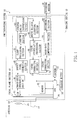
- Fig. 1 shows a block diagram of a photographing system in which an imaging device according to the present invention is installed.
- a photographing system 10 includes an imaging device 12 according to the present invention, a phototaking lens 14 attached to the imaging device 12, and a recording medium 16 connected to the imaging device 12.
- the phototaking lens 14 includes a lens group 20 and an aperture 22.
- the imaging device 12 composes an electronic camera.
- the imaging device 12 includes a release button 30, an EEPROM 32, a CPU 34, a memory (for example, DRAM) 36, a focal-plane shutter 40, a CCD 44, an image-data generating section 46, a defect pixel correcting section 48, a clamp processing section 50, a judging section 54, a striped noise suppressing section 60, a white balance adjusting section 66, a color interpolation processing section 68, a gamma correcting section 70, a color correcting section 74, an image-data compressing section 78, and a recording section 80.
- a release button 30 an EEPROM 32, a CPU 34, a memory (for example, DRAM) 36, a focal-plane shutter 40, a CCD 44, an image-data generating section 46, a defect pixel correcting section 48, a clamp processing section 50, a judging section 54, a striped noise suppressing section 60, a white balance adjusting section 66, a color interpolation processing
- the release button 30 commands the CPU 34 to start photographing.
- the EEPROM 32 stores a parameter which is necessary for controlling the imaging device 12.
- the CPU 34 controls a system of the imaging device 12 by use of the EEPROM 32 and the memory 36 (controls a section surrounded by dashed line in Fig. 1).
- the memory 36 temporarily stores image data before being converted into a predetermined format and processed.
- Fig. 2 is a block diagram showing the details of the CCD 44.
- the CCD 44 includes many pixels 84 arranged on a not-illustrated semiconductor substrate in the form of a Bayer pattern color filter array, vertical CCDs 86, a horizontal CCD 88, and a reading amplifier 90.
- Each pixel 84 includes a part of the vertical CCD 86, a sensor section 94, and a gate section for reading 96.
- the sensor section 94 is, for example, a buried photodiode which has a P-type surface region on the side of a light-receiving surface and an N-type buried region (charge accumulating region).
- the sensor section 94 generates and accumulates a pixel signal in accordance with the amount of light received.
- the pixel signal generated by the sensor section 94 is in a state of signal charge inside the pixel 84.
- each pixel 84 The side of the light-receiving surface of each pixel 84 is covered with a microlens and an optical filter.
- the optical filter selectively allows light with a wavelength of any one of red, blue, and green to pass through (not illustrated).
- a plurality of vertical CCDs 86 is formed in a direction along the arrangement of the pixels 84. Each of the vertical CCDs 86 is formed per vertical line of the sensor section 94. The signal charge is transferred from the sensor section 94 to each vertical CCD 86 through the gate section for reading 96. The vertical CCDs 86 successively transfer the signal charge to the horizontal CCD 88.
- the horizontal CCD 88 successively transfers the signal charge, which is vertically transferred from the vertical CCDs 86 in succession, to the reading amplifier 90 in a horizontal direction.
- the reading amplifier 90 amplifies the transferred signal charge with a predetermined gain, to successively input it to the image-data generating section 46.
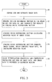
- Fig. 3 is a flowchart showing an essential part of signal processing in the foregoing imaging device 12.
- the signal processing in the imaging device 12 will be hereinafter described by following step numbers shown in Fig. 3.
- the pixel 84 selectively receiving red light is abbreviated as a red pixel.
- the pixel 84 selectively receiving blue light is abbreviated as a blue pixel, and the pixel 84 selectively receiving green light is abbreviated as a green pixel.
- a pixel signal generated by the green pixel in a row of the red pixels is abbreviated as Gr, and a pixel signal generated by the green pixel in a row of the blue pixels is abbreviated as Gb.
- a pixel signal of the red pixel horizontally adjacent to the pixel corresponding to Gb on the side of the reading amplifier 90 is abbreviated as BI
- a pixel signal of the red pixel horizontally adjacent thereto on the opposite side of the reading amplifier 90 is abbreviated as Br (refer to Gb in white text on black in Fig. 2).
- a pixel signal of the blue pixel vertically adjacent to the pixel corresponding to Gb on the side of the horizontal CCD 88 is abbreviated as Rd
- a pixel signal of the blue pixel vertically adjacent thereto on the opposite side of the horizontal CCD 88 is abbreviated as Ru.
- the CCD 44 is exposed in well-known operation.
- the image-data generating section 46 subjects an analog pixel signal outputted from the CCD 44 to correlated double sampling processing, analog-to-digital conversion, and the like, in order to generate image data.
- the image data here represents the color of each pixel as the pixel signal of a predetermined bit number. Then, image data is subjected to defect pixel correction and clamp processing, and is inputted to the judging section 54 and the striped noise suppressing section 60.
- the judging section 54 judges whether Bl>Gb is satisfied or not with respect to every Gb.
- the judging section 54 inputs the judgment result into the striped noise suppressing section 60 as table data.
- the striped noise suppressing section 60 calculates Gb', which is a modified value of Gb, with respect to each Gb. Before the explanation of this calculation, on what base the difference in the pixel signal is estimated will be described cause-by-cause.
- the effect of ringing in the output stage of the CCD 44 is considered only in Gb judged to be Bl>Gb. This is because difference in Gb caused by the ringing is negligible, when Bl is sufficiently smaller than Gb.
- Gb" Gb + Bl ⁇ Kb
- the effect of the ringing in the circuit for carrying out the correlated double sampling processing is considered only in Gb judged to be Bl>Gb, for the same reason as in the case of the equation (1). It is preferable that variation in a reference level in the circuit for carrying out the correlated double sapling processing is also considered by use of this correction coefficient Kb.
- difference caused by flare (the leak of light) on the light-receiving surface of the green pixel is estimated.
- the difference means difference in a case where light obliquely incident on the microlenses over the light-receiving surfaces of the red pixel and the blue pixel, both of which are adjacent to the green pixel corresponding to Gb, is mixed into the sensor section 94 of the green pixel.
- Gb" represents Gb after receiving the difference
- Kd and Ke represent coefficients of the difference
- Gb" satisfies the following equation.
- Gb" Gb + ⁇ (Bl + Br)/2 ⁇ ⁇ Kd + ⁇ (Ru + Rd)/2 ⁇ ⁇ Ke
- both of coefficients Kd and Ke are positive.
- the single pixel 84 including a part of the vertical CCD 86, the gate section for reading 96, and the sensor section 94 is formed in the shape of an approximately square. In other words, the sensor section 94 is longer in the vertical direction. Therefore, the vertically adjacent red pixel has the larger effect of flare on the green pixel, than the horizontally adjacent blue pixel. Thus, Ke is larger than Kd.
- the coefficient Kf is positive in the above equation. In most cases, the difference caused by the fifth reason is little in a CCD-type image sensor, and is large in a CMOS-type image sensor.
- the striped noise suppressing section 60 calculates the modified value Gb' of each Gb judged to be Bl>Gb, by use of the following equation (6). Since Gb in the equation (6) is assumed to be affected by the foregoing five reasons, Gb corresponds to Gb" in the equations (1) to (5). Therefore, Gb is corrected to the modified value Gb', by contrarily subtracting terms of the correction coefficients added in the equations (1) to (5).
- Gb' Gb - Bl ⁇ (Ka + Kb) - Rd ⁇ Kc - ⁇ (Bl + Br)/2 ⁇ ⁇ Kd - ⁇ (Ru + Rd)/2 ⁇ ⁇ (Ke + Kf)
- the striped noise suppressing section 60 calculates a modified value Gb' of each Gb which is not judged to be Bl>Gb, by use of the following equation.
- Gb' Gb - Rd ⁇ Kc - ⁇ (Bl + Br)/2 ⁇ ⁇ Kd - ⁇ (Ru + Rd)/2 ⁇ ⁇ (Ke + Kf)
- the striped noise suppressing section 60 also calculates a modified value R' of a pixel signal R of the red pixel with the use of the following equation.
- R includes both of Ru and Rd without distinction.
- R' R ⁇ ⁇ 1 + (Ke/2) + (Kf/2) ⁇
- the striped noise suppressing section 60 calculates a modified value B' of a pixel signal B of the blue pixel with the use of the following equation.
- B includes both of BI and Br without distinction.
- B' B ⁇ (1 +Kd/2)
- the striped noise suppressing section 60 corrects every signal level of Gb, R, and B to the modified values Gb', R', and B' calculated by the equations (6) to (9).
- Gr is not corrected due to the following reason.
- Gb and Gr tend to be affected by the vertically adjacent pixels rather than the horizontally adjacent pixels, except the ringing in the output stage of the CCD 44 and a correlated double sampling circuit.
- the intensity of red color is higher than that of blue color.
- Gb outputted from the pixel vertically adjacent to the red pixel tends to be larger than Gr. Therefore, when Gb is corrected to be smaller without making a correction to Gr, Gr and Gb when shooting the subject with even color become equal to each other.
- image data is subjected to white balance adjustment, color interpolation processing, gamma correction, color correction processing (for example, edge enhancing processing), and image compression (for example, JPEG conversion). Then, the recording section 80 records compressed image data on the recording medium 16.
- the coefficients Ka to Kf may be obtained by test photography using the imaging device 12, for example, during manufacturing or before shipment. After photographing a test chart the whole surface of which is evenly red, a test chart the whole surface of which is evenly blue, and the like, for example, obtained image data is analyzed to calculate the coefficients Ka to Kf. Then, obtained coefficients are rewritably stored in the EEPROM 32.
- the foregoing coefficients Ka, Kb, and Kd may be made zero, and only vertical correction may be carried out. Otherwise, when striped noise appears only in the horizontal direction, the foregoing coefficients Kc and Ke may be made zero, and only horizontal correction may be carried out.
- the coefficients Ka to Kf may be calculated one-by-one on a cause basis. For example, ringing which occurs by inputting a predetermined pulse wave into the reading amplifier 90 may be measured to obtain Ka. Otherwise, photographing a test chart in which only a single pixel is black point and the other whole pixels are illuminated by red light, signal levels outputted from the black point and peripheral pixels thereof may be measured to obtain Ke (in the case of CCD-type image sensor and Kf ⁇ 0).
- the modified value of Gb is calculated in consideration of the foregoing reasons of the difference, on the basis of the pixel signals of four pixels with different colors which are vertically and horizontally adjacent to the green pixel corresponding to Gb (step S3). Then, Gb, which tends to be larger than Gr in general, is corrected to be smaller by use of the obtained modified value (step S4). Therefore, when a subject with even color is photographed, Gb is so corrected as to be equal to Gr. In other words, it is possible to suppress line crawling without smoothing an image.
- the judging section 54 judges whether Bl>Gb is satisfied or not with respect to every Gb, and inputs the judgment result into the striped noise suppressing section 60 as table data.
- the difference by the ringing is corrected in only Gb which is judged to be Bl>Gb, on the basis that the smaller Bl is, the smaller the difference of Gb caused by the ringing will be (equation (6)). Therefore, it is possible to effectively correct the difference of Gb caused by the ringing.
- the pixel signals of the red pixel and the blue pixel are also corrected with the use of the coefficients Kd and Ke for correcting the difference of Gb caused by flare (equations (8) and (9)).
- This processing means that light, which is obliquely incident on the microlenses over the surfaces of the red pixel and the blue pixel and is mixed into the adjacent green pixel as noise, is returned to the pixel signals of the red and blue pixels. Therefore, it is possible to increase the reproducibility of the color of a photographed subject.
- the pixel signal of the red pixel is also corrected with the use of the coefficient Kf, which corrects the difference caused by the red light and infrared light reflected in the bulk (equation (9)).
- Kf the coefficient Kf
- This processing means that light, which passes through the charge accumulating region of the red pixel and is mixed into the peripheral pixels as noise, is returned to the pixel signal of the red pixel. Therefore, it is possible to increase the reproducibility of the color of a photographed subject.
- the coefficients Ka to Kf are rewritably stored in the EEPROM 32. Therefore, it is possible to repeatedly calculate and store the foregoing coefficients Ka to Kf, thereby increasing the user-friendliness. This is because it is assumed that, for example, a user who has used the imaging device 12 for the long term requests readjustment of a service center.
- the difference caused by the ringing may be corrected on the basis of the difference between the signal level of Gb and the signal level of the pixel immediately preceding Gb in transfer order.
- the foregoing equation (6) is changed to the following equation (12).
- Gb' Gb - (BI - Gb) x (Ka' + Kb') - Rd x Kc - ⁇ (Bl + Br)/2 ⁇ x Kd - ⁇ (Ru + Rd)/2 ⁇ x (Ke + Kf) ... (12)
- Ka' represents a correction coefficient which corresponds to Ka described above
- Kb' represents a correction coefficient which corresponds to Kb described above.
Landscapes
- Engineering & Computer Science (AREA)
- Multimedia (AREA)
- Signal Processing (AREA)
- Physics & Mathematics (AREA)
- Spectroscopy & Molecular Physics (AREA)
- Color Television Image Signal Generators (AREA)
- Transforming Light Signals Into Electric Signals (AREA)
Applications Claiming Priority (2)
| Application Number | Priority Date | Filing Date | Title |
|---|---|---|---|
| JP2003159459A JP4379006B2 (ja) | 2003-06-04 | 2003-06-04 | 撮像装置 |
| JP2003159459 | 2003-06-04 |
Publications (3)
| Publication Number | Publication Date |
|---|---|
| EP1484928A2 true EP1484928A2 (de) | 2004-12-08 |
| EP1484928A3 EP1484928A3 (de) | 2007-07-11 |
| EP1484928B1 EP1484928B1 (de) | 2015-03-25 |
Family
ID=33157181
Family Applications (1)
| Application Number | Title | Priority Date | Filing Date |
|---|---|---|---|
| EP04013188.0A Expired - Lifetime EP1484928B1 (de) | 2003-06-04 | 2004-06-03 | Bildaufnahmevorrichtung |
Country Status (4)
| Country | Link |
|---|---|
| US (2) | US20040246352A1 (de) |
| EP (1) | EP1484928B1 (de) |
| JP (1) | JP4379006B2 (de) |
| CN (4) | CN1574902B (de) |
Families Citing this family (12)
| Publication number | Priority date | Publication date | Assignee | Title |
|---|---|---|---|---|
| KR100825172B1 (ko) * | 2004-04-05 | 2008-04-24 | 미쓰비시덴키 가부시키가이샤 | 촬상 장치 |
| JP4717371B2 (ja) * | 2004-05-13 | 2011-07-06 | オリンパス株式会社 | 画像処理装置および画像処理プログラム |
| US7656441B2 (en) * | 2005-01-05 | 2010-02-02 | Eastman Kodak Company | Hue correction for electronic imagers |
| JP4388909B2 (ja) * | 2005-04-25 | 2009-12-24 | イーストマン コダック カンパニー | 画素欠陥補正装置 |
| US7586521B2 (en) * | 2006-01-27 | 2009-09-08 | Nethra Imaging Inc. | Automatic color calibration of an image sensor |
| KR100826215B1 (ko) * | 2006-07-25 | 2008-04-29 | 엠텍비젼 주식회사 | 격자 노이즈 및 에지 방향을 고려한 컬러 보간 방법 및장치 |
| JP4402161B1 (ja) * | 2009-03-30 | 2010-01-20 | マスレ ホールディングス エルエルピー | 撮像装置、画像再生装置、及び撮像方法 |
| JP5269016B2 (ja) * | 2010-09-10 | 2013-08-21 | 株式会社東芝 | 画像処理装置 |
| US9177983B2 (en) * | 2012-01-23 | 2015-11-03 | Omnivision Technologies, Inc. | Image sensor with optical filters having alternating polarization for 3D imaging |
| JP5648010B2 (ja) * | 2012-03-30 | 2015-01-07 | 富士フイルム株式会社 | 機器の作動方法及び撮影装置と電子内視鏡装置 |
| JP6089872B2 (ja) | 2013-03-28 | 2017-03-08 | 富士通株式会社 | 画像補正装置、画像補正方法及び生体認証装置 |
| JP6136669B2 (ja) * | 2013-07-08 | 2017-05-31 | 株式会社ニコン | 撮像装置 |
Family Cites Families (21)
| Publication number | Priority date | Publication date | Assignee | Title |
|---|---|---|---|---|
| JPS56147578A (en) | 1980-04-18 | 1981-11-16 | Nec Corp | Correction system of mixed color for solidstate color image pickup device |
| EP0131387B1 (de) * | 1983-06-15 | 1989-03-08 | Kabushiki Kaisha Toshiba | Festkörper-Bildsensor mit hoher Auflösung |
| US4701784A (en) * | 1984-06-01 | 1987-10-20 | Matsushita Electric Industrial Co., Ltd. | Pixel defect correction apparatus |
| US4945406A (en) * | 1988-11-07 | 1990-07-31 | Eastman Kodak Company | Apparatus and accompanying methods for achieving automatic color balancing in a film to video transfer system |
| ATE137377T1 (de) * | 1990-02-06 | 1996-05-15 | Canon Kk | Bildverarbeitungsgerät |
| US5668646A (en) * | 1990-02-06 | 1997-09-16 | Canon Kabushiki Kaisha | Apparatus and method for decoding differently encoded multi-level and binary image data, the later corresponding to a color in the original image |
| JP3345182B2 (ja) | 1994-08-03 | 2002-11-18 | 松下電器産業株式会社 | 固体撮像装置の駆動方法 |
| US5754678A (en) * | 1996-01-17 | 1998-05-19 | Photon Dynamics, Inc. | Substrate inspection apparatus and method |
| JP3466855B2 (ja) * | 1997-02-07 | 2003-11-17 | 株式会社リコー | 画像読取装置 |
| JP4022962B2 (ja) * | 1997-12-11 | 2007-12-19 | ソニー株式会社 | 信号処理回路および固体撮像素子の出力信号処理方法 |
| US6788340B1 (en) * | 1999-03-15 | 2004-09-07 | Texas Instruments Incorporated | Digital imaging control with selective intensity resolution enhancement |
| JP2000285229A (ja) * | 1999-03-15 | 2000-10-13 | Texas Instr Inc <Ti> | ディジタルイメージャのための不良画素フィルタリング |
| US6992712B2 (en) * | 2000-02-04 | 2006-01-31 | Olympus Optical Co., Ltd. | Imaging apparatus |
| JP4497759B2 (ja) * | 2000-06-30 | 2010-07-07 | キヤノン株式会社 | 画像処理装置及びその処理方法 |
| JP3636046B2 (ja) * | 2000-07-31 | 2005-04-06 | 株式会社日立国際電気 | 固体撮像素子の画素欠陥検出方法およびその方法を用いた撮像装置 |
| DE10042633C2 (de) * | 2000-08-30 | 2002-06-20 | Infineon Technologies Ag | Erkennung eines Geräte-Anschlußzustands beim USB |
| JP2002111989A (ja) * | 2000-10-02 | 2002-04-12 | Mega Chips Corp | 画像処理回路 |
| US6900836B2 (en) * | 2001-02-19 | 2005-05-31 | Eastman Kodak Company | Correcting defects in a digital image caused by a pre-existing defect in a pixel of an image sensor |
| US6741754B2 (en) * | 2001-02-19 | 2004-05-25 | Eastman Kodak Company | Correcting for defects in a digital image taken by an image sensor caused by pre-existing defects in two pixels in adjacent columns of an image sensor |
| US20030030738A1 (en) * | 2001-05-22 | 2003-02-13 | Clynes Steven Derrick | On-chip 2D adjustable defective pixel filtering for CMOS imagers |
| CN1186921C (zh) * | 2001-06-08 | 2005-01-26 | 光宝科技股份有限公司 | 数字信号补偿装置 |
-
2003
- 2003-06-04 JP JP2003159459A patent/JP4379006B2/ja not_active Expired - Lifetime
-
2004
- 2004-06-01 US US10/856,842 patent/US20040246352A1/en not_active Abandoned
- 2004-06-03 EP EP04013188.0A patent/EP1484928B1/de not_active Expired - Lifetime
- 2004-06-04 CN CN2004100484010A patent/CN1574902B/zh not_active Expired - Fee Related
- 2004-06-04 CN CN2010105028185A patent/CN102006487B/zh not_active Expired - Fee Related
- 2004-06-04 CN CN2010105028170A patent/CN102006486B/zh not_active Expired - Fee Related
- 2004-06-04 CN CN201010502819XA patent/CN102006488B/zh not_active Expired - Fee Related
-
2008
- 2008-10-17 US US12/285,984 patent/US7792358B2/en not_active Expired - Fee Related
Non-Patent Citations (1)
| Title |
|---|
| None |
Also Published As
| Publication number | Publication date |
|---|---|
| US20090122166A1 (en) | 2009-05-14 |
| CN102006486A (zh) | 2011-04-06 |
| CN102006488B (zh) | 2012-08-08 |
| CN102006487B (zh) | 2012-08-08 |
| EP1484928A3 (de) | 2007-07-11 |
| US7792358B2 (en) | 2010-09-07 |
| CN102006488A (zh) | 2011-04-06 |
| US20040246352A1 (en) | 2004-12-09 |
| CN1574902A (zh) | 2005-02-02 |
| CN102006487A (zh) | 2011-04-06 |
| JP4379006B2 (ja) | 2009-12-09 |
| EP1484928B1 (de) | 2015-03-25 |
| CN1574902B (zh) | 2013-06-12 |
| JP2004363902A (ja) | 2004-12-24 |
| CN102006486B (zh) | 2012-08-08 |
Similar Documents
| Publication | Publication Date | Title |
|---|---|---|
| US7792358B2 (en) | Imaging device performing color image data processing | |
| US7990447B2 (en) | Solid-state image sensor | |
| US6813046B1 (en) | Method and apparatus for exposure control for a sparsely sampled extended dynamic range image sensing device | |
| US6924841B2 (en) | System and method for capturing color images that extends the dynamic range of an image sensor using first and second groups of pixels | |
| US8300120B2 (en) | Image processing apparatus and method of processing image for reducing noise of the image | |
| US10015424B2 (en) | Method and apparatus for eliminating crosstalk amount included in an output signal | |
| US6937777B2 (en) | Image sensing apparatus, shading correction method, program, and storage medium | |
| CN1675919B (zh) | 摄像系统及图像处理方法 | |
| KR101442313B1 (ko) | 카메라 센서 교정 | |
| KR101639382B1 (ko) | 높은 동적 범위를 가지는 영상을 생성하는 장치 및 방법 | |
| EP1209903B1 (de) | Verfahren und Gerät zur Rauschunterdrückung eines spärlich abgetasteten Bildes mit erweitertem Dynamikbereich | |
| JP4768448B2 (ja) | 撮像装置 | |
| US6873442B1 (en) | Method and system for generating a low resolution image from a sparsely sampled extended dynamic range image sensing device | |
| US20090160979A1 (en) | Methods and apparatuses for double sided dark reference pixel row-wise dark level non-uniformity compensation in image signals | |
| EP1173010A2 (de) | Verfahren und Gerät zur Erweiterung des effektiven Dynamikbereichs einer Bildaufnahmevorrichtung | |
| US20030063185A1 (en) | Three-dimensional imaging with complementary color filter arrays | |
| JP4682181B2 (ja) | 撮像装置および電子情報機器 | |
| US7202895B2 (en) | Image pickup apparatus provided with image pickup element including photoelectric conversion portions in depth direction of semiconductor | |
| US20060017824A1 (en) | Image processing device, image processing method, electronic camera, and scanner | |
| JP4993275B2 (ja) | 画像処理装置 | |
| JPH0591420A (ja) | 固体撮像装置 |
Legal Events
| Date | Code | Title | Description |
|---|---|---|---|
| PUAI | Public reference made under article 153(3) epc to a published international application that has entered the european phase |
Free format text: ORIGINAL CODE: 0009012 |
|
| AK | Designated contracting states |
Kind code of ref document: A2 Designated state(s): AT BE BG CH CY CZ DE DK EE ES FI FR GB GR HU IE IT LI LU MC NL PL PT RO SE SI SK TR |
|
| AX | Request for extension of the european patent |
Extension state: AL HR LT LV MK |
|
| PUAL | Search report despatched |
Free format text: ORIGINAL CODE: 0009013 |
|
| AK | Designated contracting states |
Kind code of ref document: A3 Designated state(s): AT BE BG CH CY CZ DE DK EE ES FI FR GB GR HU IE IT LI LU MC NL PL PT RO SE SI SK TR |
|
| AX | Request for extension of the european patent |
Extension state: AL HR LT LV MK |
|
| 17P | Request for examination filed |
Effective date: 20080109 |
|
| AKX | Designation fees paid |
Designated state(s): DE FR GB |
|
| 17Q | First examination report despatched |
Effective date: 20090114 |
|
| RAP1 | Party data changed (applicant data changed or rights of an application transferred) |
Owner name: NIKON CORPORATION |
|
| GRAP | Despatch of communication of intention to grant a patent |
Free format text: ORIGINAL CODE: EPIDOSNIGR1 |
|
| INTG | Intention to grant announced |
Effective date: 20141021 |
|
| GRAS | Grant fee paid |
Free format text: ORIGINAL CODE: EPIDOSNIGR3 |
|
| GRAA | (expected) grant |
Free format text: ORIGINAL CODE: 0009210 |
|
| AK | Designated contracting states |
Kind code of ref document: B1 Designated state(s): DE FR GB |
|
| REG | Reference to a national code |
Ref country code: GB Ref legal event code: FG4D |
|
| REG | Reference to a national code |
Ref country code: DE Ref legal event code: R096 Ref document number: 602004046850 Country of ref document: DE Effective date: 20150430 |
|
| RAP2 | Party data changed (patent owner data changed or rights of a patent transferred) |
Owner name: NIKON CORPORATION |
|
| REG | Reference to a national code |
Ref country code: DE Ref legal event code: R097 Ref document number: 602004046850 Country of ref document: DE |
|
| PLBE | No opposition filed within time limit |
Free format text: ORIGINAL CODE: 0009261 |
|
| STAA | Information on the status of an ep patent application or granted ep patent |
Free format text: STATUS: NO OPPOSITION FILED WITHIN TIME LIMIT |
|
| 26N | No opposition filed |
Effective date: 20160105 |
|
| REG | Reference to a national code |
Ref country code: FR Ref legal event code: PLFP Year of fee payment: 13 |
|
| REG | Reference to a national code |
Ref country code: FR Ref legal event code: PLFP Year of fee payment: 14 |
|
| REG | Reference to a national code |
Ref country code: FR Ref legal event code: PLFP Year of fee payment: 15 |
|
| PGFP | Annual fee paid to national office [announced via postgrant information from national office to epo] |
Ref country code: DE Payment date: 20190521 Year of fee payment: 16 |
|
| PGFP | Annual fee paid to national office [announced via postgrant information from national office to epo] |
Ref country code: GB Payment date: 20190529 Year of fee payment: 16 |
|
| PGFP | Annual fee paid to national office [announced via postgrant information from national office to epo] |
Ref country code: FR Payment date: 20200512 Year of fee payment: 17 |
|
| REG | Reference to a national code |
Ref country code: DE Ref legal event code: R119 Ref document number: 602004046850 Country of ref document: DE |
|
| GBPC | Gb: european patent ceased through non-payment of renewal fee |
Effective date: 20200603 |
|
| PG25 | Lapsed in a contracting state [announced via postgrant information from national office to epo] |
Ref country code: GB Free format text: LAPSE BECAUSE OF NON-PAYMENT OF DUE FEES Effective date: 20200603 |
|
| PG25 | Lapsed in a contracting state [announced via postgrant information from national office to epo] |
Ref country code: DE Free format text: LAPSE BECAUSE OF NON-PAYMENT OF DUE FEES Effective date: 20210101 |
|
| PG25 | Lapsed in a contracting state [announced via postgrant information from national office to epo] |
Ref country code: FR Free format text: LAPSE BECAUSE OF NON-PAYMENT OF DUE FEES Effective date: 20210630 |