EP1480070B1 - Affichage à crystaux liquides à matrice TFT comprenant des électrodes à fente pour des pixel multi-domaines - Google Patents
Affichage à crystaux liquides à matrice TFT comprenant des électrodes à fente pour des pixel multi-domaines Download PDFInfo
- Publication number
- EP1480070B1 EP1480070B1 EP04004487.7A EP04004487A EP1480070B1 EP 1480070 B1 EP1480070 B1 EP 1480070B1 EP 04004487 A EP04004487 A EP 04004487A EP 1480070 B1 EP1480070 B1 EP 1480070B1
- Authority
- EP
- European Patent Office
- Prior art keywords
- electrode
- pixel
- electrodes
- substrate
- subpixel
- Prior art date
- Legal status (The legal status is an assumption and is not a legal conclusion. Google has not performed a legal analysis and makes no representation as to the accuracy of the status listed.)
- Expired - Fee Related
Links
Images

Classifications
-
- G—PHYSICS
- G02—OPTICS
- G02F—OPTICAL DEVICES OR ARRANGEMENTS FOR THE CONTROL OF LIGHT BY MODIFICATION OF THE OPTICAL PROPERTIES OF THE MEDIA OF THE ELEMENTS INVOLVED THEREIN; NON-LINEAR OPTICS; FREQUENCY-CHANGING OF LIGHT; OPTICAL LOGIC ELEMENTS; OPTICAL ANALOGUE/DIGITAL CONVERTERS
- G02F1/00—Devices or arrangements for the control of the intensity, colour, phase, polarisation or direction of light arriving from an independent light source, e.g. switching, gating or modulating; Non-linear optics
- G02F1/01—Devices or arrangements for the control of the intensity, colour, phase, polarisation or direction of light arriving from an independent light source, e.g. switching, gating or modulating; Non-linear optics for the control of the intensity, phase, polarisation or colour
- G02F1/13—Devices or arrangements for the control of the intensity, colour, phase, polarisation or direction of light arriving from an independent light source, e.g. switching, gating or modulating; Non-linear optics for the control of the intensity, phase, polarisation or colour based on liquid crystals, e.g. single liquid crystal display cells
- G02F1/133—Constructional arrangements; Operation of liquid crystal cells; Circuit arrangements
- G02F1/1333—Constructional arrangements; Manufacturing methods
- G02F1/1337—Surface-induced orientation of the liquid crystal molecules, e.g. by alignment layers
- G02F1/133707—Structures for producing distorted electric fields, e.g. bumps, protrusions, recesses, slits in pixel electrodes
-
- G—PHYSICS
- G02—OPTICS
- G02F—OPTICAL DEVICES OR ARRANGEMENTS FOR THE CONTROL OF LIGHT BY MODIFICATION OF THE OPTICAL PROPERTIES OF THE MEDIA OF THE ELEMENTS INVOLVED THEREIN; NON-LINEAR OPTICS; FREQUENCY-CHANGING OF LIGHT; OPTICAL LOGIC ELEMENTS; OPTICAL ANALOGUE/DIGITAL CONVERTERS
- G02F1/00—Devices or arrangements for the control of the intensity, colour, phase, polarisation or direction of light arriving from an independent light source, e.g. switching, gating or modulating; Non-linear optics
- G02F1/01—Devices or arrangements for the control of the intensity, colour, phase, polarisation or direction of light arriving from an independent light source, e.g. switching, gating or modulating; Non-linear optics for the control of the intensity, phase, polarisation or colour
- G02F1/13—Devices or arrangements for the control of the intensity, colour, phase, polarisation or direction of light arriving from an independent light source, e.g. switching, gating or modulating; Non-linear optics for the control of the intensity, phase, polarisation or colour based on liquid crystals, e.g. single liquid crystal display cells
- G02F1/133—Constructional arrangements; Operation of liquid crystal cells; Circuit arrangements
- G02F1/1333—Constructional arrangements; Manufacturing methods
- G02F1/1343—Electrodes
- G02F1/134309—Electrodes characterised by their geometrical arrangement
-
- G—PHYSICS
- G02—OPTICS
- G02F—OPTICAL DEVICES OR ARRANGEMENTS FOR THE CONTROL OF LIGHT BY MODIFICATION OF THE OPTICAL PROPERTIES OF THE MEDIA OF THE ELEMENTS INVOLVED THEREIN; NON-LINEAR OPTICS; FREQUENCY-CHANGING OF LIGHT; OPTICAL LOGIC ELEMENTS; OPTICAL ANALOGUE/DIGITAL CONVERTERS
- G02F1/00—Devices or arrangements for the control of the intensity, colour, phase, polarisation or direction of light arriving from an independent light source, e.g. switching, gating or modulating; Non-linear optics
- G02F1/01—Devices or arrangements for the control of the intensity, colour, phase, polarisation or direction of light arriving from an independent light source, e.g. switching, gating or modulating; Non-linear optics for the control of the intensity, phase, polarisation or colour
- G02F1/13—Devices or arrangements for the control of the intensity, colour, phase, polarisation or direction of light arriving from an independent light source, e.g. switching, gating or modulating; Non-linear optics for the control of the intensity, phase, polarisation or colour based on liquid crystals, e.g. single liquid crystal display cells
- G02F1/133—Constructional arrangements; Operation of liquid crystal cells; Circuit arrangements
- G02F1/136—Liquid crystal cells structurally associated with a semi-conducting layer or substrate, e.g. cells forming part of an integrated circuit
- G02F1/13606—Liquid crystal cells structurally associated with a semi-conducting layer or substrate, e.g. cells forming part of an integrated circuit having means for reducing parasitic capacitance
-
- G—PHYSICS
- G02—OPTICS
- G02F—OPTICAL DEVICES OR ARRANGEMENTS FOR THE CONTROL OF LIGHT BY MODIFICATION OF THE OPTICAL PROPERTIES OF THE MEDIA OF THE ELEMENTS INVOLVED THEREIN; NON-LINEAR OPTICS; FREQUENCY-CHANGING OF LIGHT; OPTICAL LOGIC ELEMENTS; OPTICAL ANALOGUE/DIGITAL CONVERTERS
- G02F1/00—Devices or arrangements for the control of the intensity, colour, phase, polarisation or direction of light arriving from an independent light source, e.g. switching, gating or modulating; Non-linear optics
- G02F1/01—Devices or arrangements for the control of the intensity, colour, phase, polarisation or direction of light arriving from an independent light source, e.g. switching, gating or modulating; Non-linear optics for the control of the intensity, phase, polarisation or colour
- G02F1/13—Devices or arrangements for the control of the intensity, colour, phase, polarisation or direction of light arriving from an independent light source, e.g. switching, gating or modulating; Non-linear optics for the control of the intensity, phase, polarisation or colour based on liquid crystals, e.g. single liquid crystal display cells
- G02F1/133—Constructional arrangements; Operation of liquid crystal cells; Circuit arrangements
- G02F1/136—Liquid crystal cells structurally associated with a semi-conducting layer or substrate, e.g. cells forming part of an integrated circuit
- G02F1/1362—Active matrix addressed cells
- G02F1/136286—Wiring, e.g. gate line, drain line
Definitions
- the present disclosure relates to a liquid crystal display and a thin film transistor array panel therefor.
- LCD liquid crystal display
- CTR cathode ray tube
- the general structure of an LCD consists of a liquid crystal (LC) layer that is positioned between pair of panels including field generating electrodes and polarizers.
- the LC layer is subject to an electric field generated by the electrodes and variations in the field strength change the molecular orientation of the LC layer. For example, upon application of an electric field, the molecules of the LC layer change their orientation and polarize light passing through the LC layer. Appropriately positioned polarized filters block the polarized light, creating dark areas that can represent desired images.
- One measure of LCD quality is viewing angle (i.e., the available area when viewing the LCD in which minimum contrast can be seen).
- Various techniques for enlarging the viewing angle have been suggested, including a technique utilizing a vertically aligned LC layer and providing cutouts or protrusions at pixel electrodes.
- cutouts and the protrusions reduce the aperture ratio (i.e., ratio between the actual size of a sub-pixel and the area of the sub-pixel that can transmit light).
- the size of the pixel electrodes be maximized.
- maximization of the size of the pixel electrodes results in a close distance between the pixel electrodes, causing strong lateral electric fields between the pixel electrodes. The strong electric fields cause unwanted altering of the orientation of the LC molecules, yielding textures and light leakage and deteriorating display characteristics.
- step-and-repeat process a single exposure area or field is called a shot.
- the shots may be misaligned due to transition, rotation, distortion, etc., which are generated during light exposure.
- parasitic capacitances generated between wires and pixel electrodes differ depending on the shots in which they are located. These capacitance differences cause a brightness difference between the shots, which is recognized at the pixels located at a boundary between the shots. As a result, a stitch defect is generated on the screen of the LCD due to the brightness discontinuity between the shots.
- US 5 040 875 A discloses an active-matrix twisted-nematic LCD having cut-outs in its counter electrode that are arranged over the data lines which lie between pixel electrodes. This reduces the electrostatic coupling between the data lines and the counter electrode. Such an electrostatic coupling leads to increased driving voltages and unnecessary light leakage in the region of the data lines. This arrangement improves device contrast ratio and reduces driving voltages.
- US 6 278 503 B1 discloses an active-matrix liquid crystal display having cut-outs (orientation control windows) in counter electrode.
- the cut-outs lie over the pixel electrodes and bisect them to create four tilt domains in a vertically aligned liquid crystal mode device.
- the data lines meander and are arranged to lie underneath the cut-out. Separate storage lines are provided.
- US 2002/113931 A1 discloses a vertically-aligned active-matrix LCD having cut-outs in both pixel and counter electrodes to create domains.
- the cut-outs in the pixel electrodes lie between those in the counter electrodes.
- the cut outs in the counter electrodes are aligned with the edges of the pixels. By influencing the formation of tilt-domains, the viewing angle is improved.
- EP 1 462 846 A discloses an active-matrix liquid crystal display having cut-outs (orientation control windows) in its counter electrode.
- the cut-outs lie over the chevron-shaped pixel electrodes and bisect them to create four tilt domains in a vertically aligned mode device.
- the data lines are also chevron-shaped.
- US 5 343 216 discloses an active-matrix TN-LCD which has divided pixel electrodes.
- a TFT-pair is arranged symmetrically about a gate electrode, each TFT switching one part of the pixel electrode.
- An electrical connection between portions of the pixel electrode can by made by exposing a connection structure with a laser. There are no cut-outs in opposing common electrode.
- US 6 476 447 B1 discloses an active-matrix LCD with two TFTs symmetrically-arranged around a gate electrode and attached to a single pixel electrode.
- the TFTs are n- and p-type channel devices, whose properties are chosen to optimise leakage current and parasitic capacitance characteristics. There are no cut-outs.
- EP 0 438 138 A discloses an active matrix LCD. Each pixel electrode is divided into two parts, each addressed by a TFT. The layout of the pixel electrode allows defect correction by laser cutting and helps to reduce the influence of the defects on the pixel capacitance. There are no cut-outs on the opposing common electrode.
- US 2002/113929 A1 discloses an active matrix LCD exhibiting line and column inversion.
- the device can be used in vertical-alignment mode.
- WO 03/044592 A an intermediate document, discloses a vertically aligned active-matrix LCD with slits in its counter electrode and a symmetric dual-drain transistor structure.
- EP 0 884 626 A2 is the closest prior art document to the invention. It discloses an active-matrix LCD of the vertically-aligned type.
- the data lines are chevron-shaped within a pixel and conform to the edge of the chevron-shaped pixel electrode; Chevron-shaped protrusions are provided on both substrates and serve to stabilize the domains in the device at intermediate voltages. There are no cut-outs.
- a liquid crystal display, in accordance with the present invention is defined in claim 1.
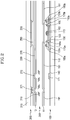
- Fig. 1 is a layout view of an LCD according to an embodiment of the present invention
- Fig. 2 is a sectional view of the LCD shown in Fig. 1 taken along the line II-II'.
- an LCD includes a TFT array panel 100, a common electrode panel 200, and an LC layer 300 interposed between the panels 100 and 200 and containing a plurality of LC molecules 310 aligned in the vertical direction with respect to the surfaces of the panels 100 and 200.
- a plurality of gate lines 121 and a plurality of storage electrode lines 131 are formed on an insulating substrate 110.
- the gate lines 121 are separated from each other and extend substantially in a transverse direction.
- the gate lines 121 transmit gate signals and a plurality of projections of each gate line 121 form a plurality of gate electrodes 123.
- Each storage electrode line 131 extends substantially in the transverse direction and includes a plurality of projections forming a plurality of pairs of storage electrodes 133a and 133b.
- the storage electrodes 133a and 133b have a shape of rectangle (or diamond) and are located close to the gate electrodes 123.
- the storage electrode lines 131 are supplied with a predetermined voltage such as a common voltage, which is applied to a common electrode 270 on the common electrode panel 200 of the LCD.
- the gate lines 121 and the storage electrode lines 131 may have a multilayered structure including two films having different physical characteristics, a lower film (not shown) and an upper film (not shown).
- the upper film is preferably made of a metal having a low resistivity, for example, an aluminum (Al) containing metal such as Al or an Al alloy, for reducing signal delay or voltage drop in the gate lines 121 and the storage electrode lines 131.
- the lower film is preferably made of a material such as chromium (Cr), molybdenum (Mo) or a Mo alloy, which has good contact characteristics with other materials such as indium tin oxide (ITO) or indium zinc oxide (IZO).
- a preferred combination of the lower film material and the upper film material is Cr and an aluminum-neodymium (Al-Nd) alloy, respectively.
- the sides of the gate lines 121 and the storage electrode lines 131 are tapered, and the angle of incline of the sides with respect to a surface of the substrate 110 ranges from about 30 to about 80 degrees.
- a gate insulating layer 140 preferably made of silicon nitride (SiNx) is formed on the gate lines 121 and the storage electrode lines 131.
- a plurality of semiconductor islands 150 preferably made of hydrogenated amorphous silicon (a-Si) or polysilicon (p-Si) are formed on the gate insulating layer 140. Each semiconductor island 150 is located opposite a gate electrode 123.
- a plurality of ohmic contact islands 163, 165a and 165b preferably made of silicide or n+ hydrogenated a-Si heavily doped with an n-type impurity are formed on the semiconductor islands 150.
- the sides of the semiconductor islands 150 and the ohmic contacts 163, 165a and 165b are tapered, and the incline angles thereof with respect to the substrate 110 are preferably in a range between about 30 to about 80 degrees.
- a plurality of data lines 171 for transmitting data voltages extend substantially in the longitudinal direction and intersect the gate lines 121 and the storage electrode lines 131.
- Each data line 171 is curved repeatedly and includes a plurality of pairs of oblique portions and a plurality of longitudinal portions.
- a pair of oblique portions are connected to each other to form a chevron and opposite ends of the pair of oblique portions are connected to respective longitudinal portions.
- the oblique portions of the data lines 171 form an angle of about 45 degrees with the gate lines 121, and the longitudinal portions cross over the gate electrodes 123.
- the length of a pair of oblique portions is about one to about nine times the length of a longitudinal portion, that is, it occupies about 50 to about 90 percent of the total length of the pair of oblique portions plus the longitudinal portion.
- the plurality of data lines 171 and a plurality of pairs of drain electrodes 175a and 175b are separated from each other and formed on the ohmic contacts 163, 165a and 165b and the gate insulating layer 140.
- the pair of drain electrodes 175a and 175b are opposite each other with respect to a longitudinal portion of a data line 171.
- Each longitudinal portion of the data lines 171 includes a plurality of projections such that the longitudinal portion including the projections forms a source electrode 173 partly enclosing the drain electrodes 175a and 175b.
- the source electrode 173 is formed on the ohmic contact 163.
- the drain electrodes 175a and 175b are formed on the ohmic contacts 165a and 165b, respectively.
- Each drain electrode 175a or 175b includes an expansion overlapping a storage electrode 133a or 133b.
- Each set of a gate electrode 123, a source electrode 173, a pair of drain electrodes 175a and 175b, and a semiconductor island 150 form a pair of TFTs.
- the pair of TFTs includes channels formed in the semiconductor island 150 disposed between the source electrode 173 and the drain electrodes 175a and 175b, respectively.
- the data lines 171 and the drain electrodes 175a and 175b may also include a lower film (not shown) preferably made of Mo, Mo alloy or Cr and an upper film (not shown) located thereon, preferably made of an Al containing metal. Further, the data lines 171 and the drain electrodes 175a and 175b also have tapered sides, with incline angles ranging from about 30 to about 80 degrees.
- a passivation layer 180 is formed on the data lines 171, the drain electrodes 175a and 175b, and exposed portions of the semiconductor islands 150 which are not covered by the data lines 171 and the drain electrodes 175a and 175b.
- the passivation layer 180 is preferably made of a flat photosensitive organic material and low dielectric insulating material such as a-Si:C:O and a-Si:O:F formed by plasma enhanced chemical vapor deposition (PECVD), or an inorganic material such as silicon nitride and silicon oxide.
- PECVD plasma enhanced chemical vapor deposition
- the passivation layer 180 may have a double-layered structure including a lower inorganic film and an upper organic film.
- the passivation layer 180 has a plurality of contact holes 185a, 185b and 189 exposing the drain electrodes 175a and 175b and end portions 179 of the data lines 171, respectively.
- the passivation layer 180 and the gate insulating layer 140 have a plurality of contact holes 182 exposing end portions 125 of the gate lines 121.
- the contact holes 182, 185a, 185b and 189 can have various shapes, such as a polygon or circle.
- the area of each contact hole 182 or 189 is preferably greater than or equal to 0.5mm ⁇ 15 ⁇ m and not larger than 2mm ⁇ 60 ⁇ m.
- the sidewalls of the contact holes 182, 185a, 185b and 189 are inclined with an angle of about 30 to about 85 degrees or have stepwise profiles.
- Each pixel electrode 191 a or 191b is located substantially in an area enclosed by the data lines 171, the gate lines 121, and the storage electrode lines 131 and forms a chevron.
- a pair of pixel electrodes 191 a and 191 b are connected to each other through a connection 193 and form a pair of subpixel areas Pa and Pb.
- the pixel electrodes 191 a and 191b are physically and electrically connected to the drain electrodes 175a and 175b through the contact holes 185a and 185b such that the pixel electrodes 191 a and 191b receive the data voltages from the drain electrodes 175a and 175b.
- the pixel electrodes 191 a and 191b supplied with the data voltages generate electric fields in cooperation with the common electrode 270, which reorient liquid crystal molecules disposed therebetween.
- a pixel electrode 191 a or 191 b and a common electrode form a capacitor called a "liquid crystal capacitor,” which stores applied voltages after turn-off of the TFT.
- the storage capacitor is implemented by overlapping the pixel electrodes 191 with the storage electrode lines 131.
- the capacitance of a storage capacitor (i.e., the storage capacitance) is increased by providing the projections at the storage electrode lines 131 forming the storage electrodes 133a and 133b, elongating the drain electrodes 175a and 175b connected to the pixel electrodes 191 a and 191 b, and providing the expansions at the drain electrodes 175a and 175b overlapping the storage electrodes 133a and 133b of the storage electrode lines 131.
- These design elements decrease the distance between the terminals and increase the overlapping areas, resulting in an increase of the storage capacitance.
- the pixel electrodes 191 a and 191b also may overlap the data lines 171 to increase aperture ratio.
- the contact assistants 192 and 199 are connected to the exposed end portions 125 of the gate lines 121 and the exposed end portions 179 of the data lines 171 through the contact holes 182 and 189, respectively.
- the contact assistants 192 and 199 are not required, but are preferred to protect the exposed portions 125 and 179 and to complement the adhesiveness of the exposed portions 125 and 179 and external devices.
- An alignment layer 11 is formed on the pixel electrodes 191 a and 191 b, the contact assistants 192 and 199, and the passivation layer 180.
- a black matrix 220 for preventing light leakage is formed on an insulating substrate 210 such as transparent glass.
- the black matrix 220 includes a plurality of openings facing the pixel electrodes 191 a and 191 b and having substantially the same shape as the pixel electrodes 191 a and 191b.
- a plurality of red, green and blue color filters 230 are formed with a substantial portion thereof in the openings of the black matrix 220 and an overcoat 250 is formed on the color filters 230.
- a common electrode 270 preferably made of transparent conductive material such as ITO and IZO is formed on the overcoat 250.
- the common electrode 270 has a plurality of cutouts 271 and 272.
- Each cutout 271 is aligned with a gap between a pair of pixel electrodes 191 a and 191b and has two main edges parallel to the two opposite edges of the pair of pixel electrodes 191 a and 191b. As shown, the cutouts 271 may overlap the edges of the pixel electrodes 191 a and 191 b.
- the cutouts 271 are provided for controlling the tilt directions of the LC molecules in the LC layer 300 and preferably have a width in a range between about 9 to about 12 microns.
- End portions of the cutouts 271 may have various shapes.
- the cutouts 272 are aligned with the data lines 171 and are provided for reducing the delay of the data voltages flowing in the data lines 171. The delay is generated by the parasitic capacitance formed by the overlap of the common electrode 270 and the data lines 171.
- the cutouts 272 are also used for controlling the tilt directions of the LC molecules of the LC layer 300.
- a homogeneous or homeotropic alignment layer 12 is coated on the common electrode 270.
- a pair of polarizers (not shown) are provided on the outer surfaces of the panels 100 and 200 such that their transmissive axes are crossed and one of the transmissive axes is parallel to the gate lines 121.
- the LCD may further include at least one retardation film (e.g., an optical element that produces, for example, full, half or quarter wave phase changes of polarized light) for compensating for the retardation of the LC layer 300.
- at least one retardation film e.g., an optical element that produces, for example, full, half or quarter wave phase changes of polarized light
- the LC molecules in the LC layer 300 are aligned such that their long axes are vertical to the surfaces of the panels 100 and 200.
- the liquid crystal layer 300 has negative dielectric anisotropy.
- LC molecules tend to change their orientations in response to the electric field such that their long axes are perpendicular to the field direction.
- the horizontal component of the primary electric field adopts four different orientations, thereby forming four domains in the LC layer 300 with different LC molecule tilt directions.
- the horizontal component is perpendicular to the first and second edges of the cutouts 271, perpendicular to the edge of the pixel electrode 191 a and perpendicular to the edge of the pixel electrode 191 b. Accordingly, four domains having different tilt directions are formed in the LC layer 300.
- cutouts 271 may be substituted with a plurality of protrusions formed on the common electrode 270 since the tilt directions of the LC molecules also can be controlled by a plurality of protrusions (not shown).
- the directions of a secondary electric field due to the voltage difference between the pixel electrodes 191 a and 191 b are perpendicular to each of the edges of the cutouts 271. Accordingly, the field direction of the secondary electric field coincides with that of the horizontal component of the primary electric field. Consequently, the secondary electric field between the pixel electrodes 191 a and 191 b enhances the tilt directions of the LC molecules.
- a secondary electric field that enhances the tilt directions of the LC molecules is attained by supplying an adjacent pixel electrode with a data voltage having opposite polarity with respect to the common voltage.
- a direction of the secondary electric field generated between adjacent pixel electrodes is equivalent to the horizontal component of the primary electric field generated between the common and pixel electrodes.
- a secondary electric field between the adjacent pixel electrodes can be generated to enhance the stability of the domains.
- the tilt directions of all the domains form an angle of about 45 degrees with the gate lines 121, and the gate lines 121 are parallel to or perpendicular to the edges of the panels 100 and 200. Since a 45-degree intersection of the tilt directions and transmissive axes of the polarizers results in maximum transmittance, the polarizers can be attached such that the transmissive axes of the polarizers are parallel or perpendicular to the edges of the panels 100 and 200, thereby reducing the production cost.
- a plurality of gate lines 121 including a plurality of gate electrodes 123 and a plurality of storage electrode lines 131 including a plurality of storage electrodes 133a and 133b are formed on an insulating substrate 110 such as transparent glass.
- the gate lines 121 and the storage electrode lines 131 have a double-layered structure including a lower conductive film and an upper conductive film
- the lower conductive film is preferably made of material such as a Cr or Mo alloy having good physical and chemical characteristics
- the upper conductive film is preferably made of Al or an Al containing metal.
- a gate insulating layer 140 having a thickness of about 1,500 to about 5,000 ⁇ , an intrinsic a-Si layer with a thickness of about 500 to about 2,000 ⁇ , and an extrinsic a-Si layer with a thickness of about 300 to about 600 ⁇ are photo-etched to form a plurality of extrinsic semiconductor islands and a plurality of intrinsic semiconductor islands 150 on the gate insulating layer 140.
- a plurality of data lines 171 including a plurality of source electrodes 173 and a plurality of drain electrodes 175a and 175b are formed.
- portions of the extrinsic semiconductor islands which are not covered with the data lines 171 and the drain electrodes 175a and 175b, are removed to complete a plurality of ohmic contact islands 163 and 165 and to expose portions of the intrinsic semiconductor islands 150.
- Oxygen plasma treatment preferably follows thereafter in order to stabilize the exposed surfaces of the semiconductor islands 150.
- a passivation layer 180 is formed of a photosensitive organic insulating material such as acryl-based material and is deposited on the existing structure. After depositing the passivation layer 180, the passivation layer 180 and the gate insulating layer 140 are patterned to form a plurality of contact holes 182, 185a, 185b and 189 exposing end portions 125 of the gate lines 121, the drain electrodes 175a and 17bb, and end portions 179 of the data lines 171, respectively.
- a plurality of pixel electrodes 191 a and 191b and a plurality of contact assistants 192 and 199 are formed on the passivation layer 180 by sputtering and photo-etching an IZO or ITO layer with a thickness of about 400 to about 500 ⁇ .
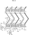
- Fig. 3 is a layout view of an LCD not according to the present invention
- Fig. 4 is a sectional view of the LCD shown in Fig. 3 taken along the line IV-VI'.
- a layered structure of a TFT array panel of this LCD includes some of the same elements as shown in Figs. 1 and 2 .
- a plurality of gate lines 121 including a plurality of gate electrodes 123 and a plurality of storage electrodes lines 131 including a plurality of storage electrodes 133a and 133b are formed on a substrate 110.
- a gate insulating layer 140, a plurality of semiconductor stripes 152, and a plurality of ohmic contact stripes and islands 163 and 165 are sequentially formed on the substrate 110 including the gate lines 121, gate electrodes 123, storage electrode lines 131 and storage electrodes 133a, 133b.
- a plurality of data lines 171 including a plurality of source electrodes 173 and a plurality of drain electrodes 175a and 175b are formed on the ohmic contacts 163 and 165, and a passivation layer 180 and an alignment layer 11 are sequentially formed thereon.
- a plurality of contact holes 182, 185a, 185b and 189 are provided in the passivation layer 180 and/or the gate insulating layer 140, and a plurality of pixel electrodes 191a and 191b and a plurality of contact assistants 192 and 199 are formed on the passivation layer 180.
- a layered structure of a common electrode panel of the LCD shown in Fig. 4 includes some of the same elements as shown in Figs. 1 and 2 .
- a black matrix 220, an overcoat 250, and a common electrode 270 as well as an alignment layer 21 are sequentially formed on an insulating substrate 210.
- the TFT array panel shown in Figs. 3 and 4 extends the semiconductor stripes 152 and the ohmic contacts 163 along the data lines 171. Also, the semiconductor stripes 152 have almost the same planar shapes as the data lines 171 and the drain electrodes 175a and 175b as well as the underlying ohmic contacts 163 and 165, except for channel portions of the TFTs.
- a plurality of red, green and blue color filters R, G and B are formed under the passivation layer 180 opposite the pixel electrodes 191a and 191b, and there is no color filter on the upper panel 200. Further, the contact holes 185a and 185b penetrate the color filters R, G and B. Two adjacent color filters of the color filters R, G and B may overlap each other to enhance the prevention of light leakage.
- a manufacturing method of TFT array panel this simultaneously forms the data lines 171, the drain electrodes 175a and 175b, the semiconductor stripes 152, and the ohmic contacts 163 and 165 using one photolithography process.
- a photoresist pattern for the photolithography process has position-dependent thickness, and in particular, it has portions with smaller thickness located on the channels of TFTs. Therefore, additional photolithography processes can be omitted to simplify the manufacturing process.
Claims (10)
- Écran à cristaux liquides, comprenant :un panneau (100), composé de réseaux de transistors à couches minces, comportant un premier substrat (110) ;un panneau (200) d'électrodes de référence, comportant un second substrat (210) ;une couche (300) de cristaux liquides, interposée entre le panneau (100), composé de réseaux de transistors à couches minces et le panneau (200) d'électrodes de référence, la couche (300) de cristaux liquides contenant une pluralité de molécules (310) de cristaux liquides, qui sont alignées, en l'absence d'un champ électrique appliqué, dans le sens vertical par rapport aux surfaces du panneau (100), composé de réseaux de transistors à couches minces et du panneau (200) d'électrodes de référence ;une pluralité d'électrodes de pixels (191), agencées sur le premier substrat (110), chaque électrode de pixel (191) définissant un pixel, dans lequel chaque électrode de pixel (191) comprend une paire d'électrodes de sous-pixels (191a, 191b), constituées d'une première électrode de sous-pixels (191a) et d'une seconde électrode de sous-pixels (191b), séparées par un premier interstice etune électrode de référence (270), agencée sur ledit second substrat (210) ;dans lequel le second substrat (210) est éloigné du premier substrat (110) par un deuxième interstice ;dans lequel une pluralité de découpes (271, 272), comprenant des premières découpes (272) et des secondes découpes (271), est prévue dans l'électrode de référence (270),dans lequel en outre chaque première découpe (272) est alignée avec le premier interstice entre les première et seconde électrodes de sous-pixels (191a, 191b) dans chaque paire d'électrodes de sous-pixels (191a, 191b),dans lequel la première découpe (272) comporte un premier bord principal, aligné parallèlement au bord de la première électrode de sous-pixels, voisine de la seconde électrode de sous-pixels (191b) et un second bord principal, aligné parallèlement au bord de la seconde électrode de sous-pixels, (191b), voisine du premier sous-pixel (191a) ;dans lequel l'écran à cristaux liquide comprend en outre :une pluralité de lignes de données (171), destinées à émettre des tensions de données, s'étendant dans une première direction longitudinale sur le premier substrat (110),dans lequel les premières découpes (272) sont alignées avec la pluralité de lignes de données (171) etdans lequel les première et seconde électrodes de sous-pixels (191a, 191b) dans chaque paire d'électrodes de sous-pixels (191a, 191b) sont disposées de part et d'autre de la ligne de données (171) dans le pixel, c'est-à-dire qu'un élément de la pluralité de ligne de données (171) est interposé entre les première et seconde électrodes de sous-pixels (191a, 191 b) dans chaque paire d'électrodes de sous-pixels (191 a, 191 b) ;une pluralité de lignes de grilles (121), destinées à émettre des signaux de grilles, s'étendant dans une seconde direction sensiblement transversale sur le premier substrat (110) ;une pluralité d'électrodes de stockage (131), destinées à émettre au moins une tension prédéterminée, s'étendant aussi dans la seconde direction sensiblement transversale sur le premier substrat (110) etune pluralité de transistors à couches minces, agencée sur le premier substrat (110), de sorte qu'il y a un transistor à couche mince dans chaque pixel, dans lequel chaque transistor à couche mince comporte des première et seconde électrodes de drain (175a, 175b),dans lequel en outre les première et seconde électrodes de drain (175a, 175b) sont agencées sensiblement symétriquement de part et d'autre d'une partie longitudinale de la ligne de données (171) dans chaque pixel,de sorte que les première et seconde électrodes de sous-pixels (191 a, 191b) sont reliées respectivement aux première et seconde électrodes de drain (175a, 175b),dans lequel en outre les première et secondes électrodes de sous-pixels (191a, 191b), chacune ayant respectivement une première zone de sous-pixels (Pa) et une seconde zone de sous-pixels (Pb), sont reliées électriquement entre elles par le biais d'une connexion (193) ;les première et secondes électrodes de sous-pixels (191a, 191b) étant séparées par la ligne de données (171) dans chaque pixel et étant délimitées par deux lignes de grille adjacentes (121),dans lequel les première et secondes électrodes de sous-pixels (191a, 191b) ont chacune une forme de chevron,dans lequel chaque seconde découpe (271) est agencée sur le troisième interstice en forme de chevron, entre les électrodes de pixels (191), qui sont immédiatement voisines les unes des autres dans la seconde direction,dans lequel chaque ligne de données de la pluralité de lignes de données (171) est recourbée à plusieurs reprises et est constituée d'une pluralité de paires de parties obliques et d'une pluralité de parties longitudinales, les parties longitudinales s'étendant dans la première direction longitudinale, de sorte que, dans chaque pixel, deux parties obliques formant paire sont reliées l'une à l'autre, pour former une partie en forme de chevron, qui est reliée elle-même, à ses extrémités opposées, à des parties longitudinales respectives.
- Écran à cristaux liquides selon la revendication 1, dans lequel la seconde découpe (271) a une largeur dans la plage d'environ 9 à environ 12 microns.
- Écran à cristaux liquides selon la revendication 1, dans lequel, dans chaque pixel, la première électrode de sous-pixels (191 a) et la seconde électrode (191b) chevauchent la ligne de données (171).
- Écran à cristaux liquides selon la revendication 1, dans lequel la pluralité de lignes de données (171) croise la pluralité de lignes de grilles (121) et la pluralité de lignes de stockage (131).
- Écran à cristaux liquides selon la revendication 1, dans lequel au moins un élément parmi la pluralité de lignes de grilles (121), la pluralité de lignes d'électrodes de stockage (131) et la pluralité de lignes de données (171) comporte des côtés effilés, dans lesquelles l'angle d'inclinaison des côtés effilés se situe, par rapport à une surface horizontale du premier substrat (110), vu en coupe transversale, dans la plage d'environ 30 à environ 80 degrés.
- Écran à cristaux liquides selon la revendication 1, dans lequel au moins un élément parmi la pluralité de lignes de grilles (121), la pluralité de lignes d'électrodes de stockage (131) et la pluralité de lignes de données (171) comporte une couche inférieure sous une couche supérieure, vu en coupe transversale.
- Écran à cristaux liquides selon la revendication 6, dans lequel la couche supérieure comporte un élément parmi de l'aluminium et un alliage d'aluminium, tandis que la couche inférieure comporte un élément parmi du chrome, du molybdène et un alliage de molybdène.
- Écran à cristaux liquides selon la revendication 1, comprenant en outre :une pluralité d'électrodes de grilles (123), chacune d'elles étant une projection depuis une ligne de grilles (121), agencée sur le premier substrat (110), de sorte que chaque pixel comprend une électrode de grille (123) ;une pluralité de paires de première et seconde électrodes de stockage (133a, 133b), chaque électrode de stockage (133a, 133b) étant une projection depuis une ligne de stockage (131), agencée sur le premier substrat (110), de sorte que chaque pixel comprend une paire d'électrodes de stockage, constituée d'une première électrode de stockage (133a) et d'une seconde électrode de stockage (133b), qui ont une forme rectangulaire ou en losange et sont situées près de l'électrode de grille (123) dans le pixel ;dans lequel des extensions des première et seconde électrodes de drain (175a, 175b) chevauchent respectivement les première et seconde électrodes de stockage (133a, 133b).
- Écran à cristaux liquides selon la revendication 1, comprenant en outre une pluralité de filtres colorés (230), formés sur un élément parmi le premier substrat (110) et le second substrat (210), dans lequel deux filtres colorés adjacents de la pluralité de filtres colorés (230) se chevauchent mutuellement.
- Écran à cristaux liquides selon la revendication 1, comprenant en outre :une couche d'isolation de grille (140), agencée sur les lignes de grilles (121) et les lignes d'électrodes de stockage (131) sur le premier substrat (110) ;une pluralité d'îlots semi-conducteurs (150), formée sur la couche d'isolation de grille (140), de sorte qu'il y a un îlot semi-conducteur dans chaque pixel qui est agencé en face de l'électrode de grille (123) dans ce pixel ;une pluralité de contacts ohmiques (163, 165a, 165b), agencés sur les îlots semi-conducteurs (150), de sorte qu'il y a trois contacts ohmiques (163, 165a, 165b) sur l'îlot semi-conducteur (150) dans chaque pixel ;dans lequel, dans chaque pixel, les électrodes de drain (175a, 17b) sont agencées sur deux des contacts ohmiques (165a, 165b) et dans lequel en outre la ligne de données (171) dans chaque pixel est agencée sur l'un des contacts ohmiques (163) et sur la couche d'isolation de grille (140).
Applications Claiming Priority (2)
| Application Number | Priority Date | Filing Date | Title |
|---|---|---|---|
| KR2003031841 | 2003-05-20 | ||
| KR1020030031841A KR100569718B1 (ko) | 2003-05-20 | 2003-05-20 | 다중 도메인 액정 표시 장치 |
Publications (3)
| Publication Number | Publication Date |
|---|---|
| EP1480070A2 EP1480070A2 (fr) | 2004-11-24 |
| EP1480070A3 EP1480070A3 (fr) | 2005-08-17 |
| EP1480070B1 true EP1480070B1 (fr) | 2017-06-07 |
Family
ID=36970435
Family Applications (1)
| Application Number | Title | Priority Date | Filing Date |
|---|---|---|---|
| EP04004487.7A Expired - Fee Related EP1480070B1 (fr) | 2003-05-20 | 2004-02-27 | Affichage à crystaux liquides à matrice TFT comprenant des électrodes à fente pour des pixel multi-domaines |
Country Status (6)
| Country | Link |
|---|---|
| US (3) | US7046323B2 (fr) |
| EP (1) | EP1480070B1 (fr) |
| JP (1) | JP4733363B2 (fr) |
| KR (1) | KR100569718B1 (fr) |
| CN (2) | CN100414406C (fr) |
| TW (1) | TWI341408B (fr) |
Families Citing this family (17)
| Publication number | Priority date | Publication date | Assignee | Title |
|---|---|---|---|---|
| JP4550484B2 (ja) * | 2003-05-13 | 2010-09-22 | 三星電子株式会社 | 薄膜トランジスタ表示板及びこれを含む多重ドメイン液晶表示装置 |
| KR101006436B1 (ko) * | 2003-11-18 | 2011-01-06 | 삼성전자주식회사 | 표시 장치용 박막 트랜지스터 표시판 |
| JP2005258414A (ja) * | 2004-02-12 | 2005-09-22 | Seiko Instruments Inc | 液晶表示装置およびその製造方法 |
| TWI379113B (en) * | 2004-07-07 | 2012-12-11 | Samsung Display Co Ltd | Array substrate, manufacturing method thereof and display device having the same |
| KR101337265B1 (ko) * | 2004-12-27 | 2013-12-05 | 삼성디스플레이 주식회사 | 박막 트랜지스터 표시판 및 이를 포함하는 액정 표시 장치 |
| TWI399598B (zh) * | 2004-12-27 | 2013-06-21 | Samsung Display Co Ltd | 液晶顯示器 |
| KR20070051045A (ko) * | 2005-11-14 | 2007-05-17 | 삼성전자주식회사 | 액정 표시 장치 |
| KR101201969B1 (ko) | 2005-12-23 | 2012-11-15 | 삼성디스플레이 주식회사 | 액정 표시 장치 |
| US8144291B2 (en) * | 2006-07-20 | 2012-03-27 | Sharp Kabushiki Kaisha | Display device and production method thereof |
| KR101300184B1 (ko) | 2006-08-03 | 2013-08-26 | 삼성디스플레이 주식회사 | 액정 표시 장치 |
| US8125584B2 (en) | 2007-01-17 | 2012-02-28 | Sharp Kabushiki Kaisha | Liquid crystal display panel and liquid crystal display device |
| KR101427708B1 (ko) * | 2007-02-01 | 2014-08-11 | 삼성디스플레이 주식회사 | 액정 표시 패널 |
| JP5079448B2 (ja) * | 2007-10-24 | 2012-11-21 | 株式会社ジャパンディスプレイウェスト | 液晶装置及びそれを備えた電子機器 |
| WO2009130819A1 (fr) * | 2008-04-22 | 2009-10-29 | シャープ株式会社 | Dispositif d'affichage à cristaux liquides |
| CN102608815A (zh) * | 2012-03-22 | 2012-07-25 | 深圳市华星光电技术有限公司 | 液晶显示面板以及其制造方法 |
| KR20140111874A (ko) * | 2013-03-12 | 2014-09-22 | 삼성디스플레이 주식회사 | 액정 표시 장치 |
| JP2014222483A (ja) * | 2013-05-14 | 2014-11-27 | 株式会社ジャパンディスプレイ | 電子部品 |
Citations (1)
| Publication number | Priority date | Publication date | Assignee | Title |
|---|---|---|---|---|
| EP0884626A2 (fr) * | 1997-06-12 | 1998-12-16 | Fujitsu Limited | Dispositif d'affichage à cristal liquide d'orientation verticale |
Family Cites Families (35)
| Publication number | Priority date | Publication date | Assignee | Title |
|---|---|---|---|---|
| JP2605723B2 (ja) * | 1987-07-22 | 1997-04-30 | 日本電気株式会社 | 薄膜トランジスタアレー形液晶表示装置 |
| US5343216A (en) * | 1989-01-31 | 1994-08-30 | Sharp Kabushiki Kaisha | Active matrix substrate and active matrix display apparatus |
| DE69108062T2 (de) * | 1990-01-17 | 1995-07-20 | Toshiba Kawasaki Kk | Flüssigkristall-Anzeigevorrichtung mit aktiver Matrix. |
| JP2669954B2 (ja) * | 1991-05-08 | 1997-10-29 | シャープ株式会社 | アクティブマトリクス表示装置 |
| TW476451U (en) * | 1991-08-23 | 2002-02-11 | Semiconductor Energy Lab | Semiconductor device |
| US5193018A (en) * | 1991-10-28 | 1993-03-09 | Industrial Technology Research Institute | Active matrix liquid crystal display system using complementary thin film transistors |
| US5485019A (en) * | 1992-02-05 | 1996-01-16 | Semiconductor Energy Laboratory Co., Ltd. | Semiconductor device and method for forming the same |
| US5434690A (en) * | 1993-07-27 | 1995-07-18 | Kabushiki Kaisha Toshiba | Liquid crystal device with pixel electrodes in an opposed striped form |
| DE69434302T2 (de) * | 1993-07-27 | 2005-12-29 | Sharp K.K. | Flüssigkristall-Anzeigevorrichtung |
| JP3367176B2 (ja) * | 1993-11-04 | 2003-01-14 | ジェイエスアール株式会社 | 熱可塑性ノルボルネン系樹脂成形品の製造方法 |
| CN1105328A (zh) | 1994-11-09 | 1995-07-19 | 王浩 | 将自行车改装成三轮车的多用途车 |
| JPH10186366A (ja) * | 1996-12-26 | 1998-07-14 | Fujitsu Ltd | 液晶表示装置 |
| KR19990026575A (ko) | 1997-09-25 | 1999-04-15 | 윤종용 | 화소 결함 구제 구조를 갖는 액정 표시 장치용 박막 트랜지스터기판 |
| US7301595B2 (en) * | 1997-10-01 | 2007-11-27 | Sanyo Electric Co., Ltd. | Vertically aligned liquid crystal display |
| KR100309918B1 (ko) * | 1998-05-16 | 2001-12-17 | 윤종용 | 광시야각액정표시장치및그제조방법 |
| KR100354904B1 (ko) * | 1998-05-19 | 2002-12-26 | 삼성전자 주식회사 | 광시야각액정표시장치 |
| JP3427729B2 (ja) * | 1998-05-26 | 2003-07-22 | 松下電器産業株式会社 | 液晶表示装置、液晶表示装置用基板、及びその製造方法 |
| KR100312753B1 (ko) * | 1998-10-13 | 2002-04-06 | 윤종용 | 광시야각액정표시장치 |
| US6900869B1 (en) * | 1998-11-25 | 2005-05-31 | Lg. Philips Lcd Co., Ltd. | Multi-domain liquid crystal display device with particular dielectric structures |
| US7119870B1 (en) | 1998-11-27 | 2006-10-10 | Sanyo Electric Co., Ltd. | Liquid crystal display device having particular drain lines and orientation control window |
| JP3378820B2 (ja) * | 1999-01-20 | 2003-02-17 | 三洋電機株式会社 | 垂直配向型液晶表示装置 |
| KR100357216B1 (ko) * | 1999-03-09 | 2002-10-18 | 엘지.필립스 엘시디 주식회사 | 멀티도메인 액정표시소자 |
| KR100635940B1 (ko) * | 1999-10-29 | 2006-10-18 | 삼성전자주식회사 | 수직 배향형 액정 표시 장치 |
| KR100504532B1 (ko) * | 1999-12-28 | 2005-08-03 | 엘지.필립스 엘시디 주식회사 | 멀티도메인 액정표시소자 |
| KR100840308B1 (ko) * | 2000-06-13 | 2008-06-20 | 삼성전자주식회사 | 도메인 크기가 최적화된 수직 배향 액정 표시 장치 |
| KR100729762B1 (ko) | 2000-11-14 | 2007-06-20 | 삼성전자주식회사 | 측면 대비비 및 측면 색재현성을 향상시킨 액정 표시 장치 |
| TW573166B (en) * | 2000-12-13 | 2004-01-21 | Au Optronics Corp | Wide viewing angle liquid crystal display |
| TWI264604B (en) * | 2001-02-19 | 2006-10-21 | Seiko Epson Corp | Active-matrix liquid crystal display and electronic device therefor |
| JP2002357843A (ja) * | 2001-06-04 | 2002-12-13 | Matsushita Electric Ind Co Ltd | 液晶表示パネル |
| JP4019697B2 (ja) | 2001-11-15 | 2007-12-12 | 株式会社日立製作所 | 液晶表示装置 |
| EP1313220A1 (fr) | 2001-11-19 | 2003-05-21 | Motorola, Inc. | Appareil pour générer des signaux d'horloge multiples à caractéristiques différentes |
| KR20030042221A (ko) * | 2001-11-22 | 2003-05-28 | 삼성전자주식회사 | 액정 표시 장치용 박막 트랜지스터 기판 |
| KR100848087B1 (ko) | 2001-12-11 | 2008-07-24 | 삼성전자주식회사 | 기판 위에 패턴을 형성하는 방법 및 이를 이용한 액정표시 장치용 기판의 제조 방법 |
| US6922183B2 (en) * | 2002-11-01 | 2005-07-26 | Chin-Lung Ting | Multi-domain vertical alignment liquid crystal display and driving method thereof |
| KR100929675B1 (ko) | 2003-03-24 | 2009-12-03 | 삼성전자주식회사 | 다중 도메인 액정 표시 장치 및 그 박막 트랜지스터 기판 |
-
2003
- 2003-05-20 KR KR1020030031841A patent/KR100569718B1/ko not_active IP Right Cessation
-
2004
- 2004-02-17 US US10/780,335 patent/US7046323B2/en not_active Expired - Fee Related
- 2004-02-27 EP EP04004487.7A patent/EP1480070B1/fr not_active Expired - Fee Related
- 2004-03-01 TW TW093105291A patent/TWI341408B/zh not_active IP Right Cessation
- 2004-03-26 CN CNB2004100312137A patent/CN100414406C/zh not_active Expired - Fee Related
- 2004-03-26 CN CN2008101448715A patent/CN101329482B/zh not_active Expired - Fee Related
- 2004-05-19 JP JP2004148737A patent/JP4733363B2/ja not_active Expired - Fee Related
-
2006
- 2006-05-12 US US11/433,319 patent/US7872700B2/en not_active Expired - Fee Related
-
2011
- 2011-01-14 US US13/007,097 patent/US8334958B2/en not_active Expired - Fee Related
Patent Citations (1)
| Publication number | Priority date | Publication date | Assignee | Title |
|---|---|---|---|---|
| EP0884626A2 (fr) * | 1997-06-12 | 1998-12-16 | Fujitsu Limited | Dispositif d'affichage à cristal liquide d'orientation verticale |
Also Published As
| Publication number | Publication date |
|---|---|
| KR20040099749A (ko) | 2004-12-02 |
| EP1480070A2 (fr) | 2004-11-24 |
| TW200502631A (en) | 2005-01-16 |
| US7872700B2 (en) | 2011-01-18 |
| US20040233367A1 (en) | 2004-11-25 |
| CN101329482B (zh) | 2011-11-16 |
| JP2004348131A (ja) | 2004-12-09 |
| CN1573479A (zh) | 2005-02-02 |
| CN101329482A (zh) | 2008-12-24 |
| US7046323B2 (en) | 2006-05-16 |
| US8334958B2 (en) | 2012-12-18 |
| US20060203173A1 (en) | 2006-09-14 |
| KR100569718B1 (ko) | 2006-04-10 |
| TWI341408B (en) | 2011-05-01 |
| US20110109825A1 (en) | 2011-05-12 |
| CN100414406C (zh) | 2008-08-27 |
| EP1480070A3 (fr) | 2005-08-17 |
| JP4733363B2 (ja) | 2011-07-27 |
Similar Documents
| Publication | Publication Date | Title |
|---|---|---|
| US7872700B2 (en) | Liquid crystal display and thin film transistor array panel therefor | |
| EP1621924B1 (fr) | Affichage à cristaux liquides et son panneau | |
| US7379142B2 (en) | Liquid crystal display | |
| US7995017B2 (en) | Liquid crystal display and thin film transistor array panel therefor | |
| US8253913B2 (en) | Liquid crystal display and thin film transistor array panel therefor | |
| US7632692B2 (en) | Liquid crystal display, thin film transistor array panel therefor, and manufacturing method thereof | |
| US7894026B2 (en) | Thin film transistor array panel and liquid crystal display including light shield | |
| US7545472B2 (en) | Liquid crystal display and thin film transistor substrate therefor | |
| US7292303B2 (en) | Liquid crystal display and panel therefor including regular and successive regular domain defining members | |
| TWI382255B (zh) | 液晶顯示器及其面板 | |
| US20040233343A1 (en) | Liquid crystal display and thin film transistor array panel therefor | |
| US20060192906A1 (en) | Thin film transistor array panel and manufacturing method thereof | |
| US7408200B2 (en) | Thin film transistor array panel and manufacturing method thereof | |
| EP1643298B1 (fr) | Procédé de fabrication d'un écran à cristaux liquides et masque à utiliser dans celui-ci | |
| KR20050036128A (ko) | 다중 도메인 액정 표시 장치 | |
| US7474363B2 (en) | Liquid crystal display and panel therefor | |
| JP2004348131A5 (fr) | ||
| US7538842B2 (en) | Liquid crystal display panel with aligning members parallel to data lines that are either electrically floating or at substantially the same voltage as the data lines |
Legal Events
| Date | Code | Title | Description |
|---|---|---|---|
| PUAI | Public reference made under article 153(3) epc to a published international application that has entered the european phase |
Free format text: ORIGINAL CODE: 0009012 |
|
| AK | Designated contracting states |
Kind code of ref document: A2 Designated state(s): AT BE BG CH CY CZ DE DK EE ES FI FR GB GR HU IE IT LI LU MC NL PT RO SE SI SK TR |
|
| AX | Request for extension of the european patent |
Extension state: AL LT LV MK |
|
| PUAL | Search report despatched |
Free format text: ORIGINAL CODE: 0009013 |
|
| RIC1 | Information provided on ipc code assigned before grant |
Ipc: 7G 02F 1/1362 B Ipc: 7G 02F 1/139 B Ipc: 7G 02F 1/1343 A Ipc: 7G 02F 1/1368 B |
|
| AK | Designated contracting states |
Kind code of ref document: A3 Designated state(s): AT BE BG CH CY CZ DE DK EE ES FI FR GB GR HU IE IT LI LU MC NL PT RO SE SI SK TR |
|
| AX | Request for extension of the european patent |
Extension state: AL LT LV MK |
|
| 17P | Request for examination filed |
Effective date: 20060203 |
|
| AKX | Designation fees paid |
Designated state(s): DE FR GB |
|
| RAP1 | Party data changed (applicant data changed or rights of an application transferred) |
Owner name: SAMSUNG ELECTRONICS CO., LTD. |
|
| RAP1 | Party data changed (applicant data changed or rights of an application transferred) |
Owner name: SAMSUNG DISPLAY CO., LTD. |
|
| RAP1 | Party data changed (applicant data changed or rights of an application transferred) |
Owner name: SAMSUNG DISPLAY CO., LTD. |
|
| GRAP | Despatch of communication of intention to grant a patent |
Free format text: ORIGINAL CODE: EPIDOSNIGR1 |
|
| STAA | Information on the status of an ep patent application or granted ep patent |
Free format text: STATUS: GRANT OF PATENT IS INTENDED |
|
| INTG | Intention to grant announced |
Effective date: 20161213 |
|
| GRAS | Grant fee paid |
Free format text: ORIGINAL CODE: EPIDOSNIGR3 |
|
| GRAA | (expected) grant |
Free format text: ORIGINAL CODE: 0009210 |
|
| STAA | Information on the status of an ep patent application or granted ep patent |
Free format text: STATUS: THE PATENT HAS BEEN GRANTED |
|
| AK | Designated contracting states |
Kind code of ref document: B1 Designated state(s): DE FR GB |
|
| REG | Reference to a national code |
Ref country code: GB Ref legal event code: FG4D |
|
| GRAA | (expected) grant |
Free format text: ORIGINAL CODE: 0009210 |
|
| REG | Reference to a national code |
Ref country code: DE Ref legal event code: R096 Ref document number: 602004051351 Country of ref document: DE |
|
| REG | Reference to a national code |
Ref country code: FR Ref legal event code: PLFP Year of fee payment: 15 |
|
| REG | Reference to a national code |
Ref country code: DE Ref legal event code: R097 Ref document number: 602004051351 Country of ref document: DE |
|
| PLBE | No opposition filed within time limit |
Free format text: ORIGINAL CODE: 0009261 |
|
| STAA | Information on the status of an ep patent application or granted ep patent |
Free format text: STATUS: NO OPPOSITION FILED WITHIN TIME LIMIT |
|
| 26N | No opposition filed |
Effective date: 20180308 |
|
| PGFP | Annual fee paid to national office [announced via postgrant information from national office to epo] |
Ref country code: GB Payment date: 20200123 Year of fee payment: 17 Ref country code: DE Payment date: 20200121 Year of fee payment: 17 |
|
| PGFP | Annual fee paid to national office [announced via postgrant information from national office to epo] |
Ref country code: FR Payment date: 20200123 Year of fee payment: 17 |
|
| REG | Reference to a national code |
Ref country code: DE Ref legal event code: R119 Ref document number: 602004051351 Country of ref document: DE |
|
| GBPC | Gb: european patent ceased through non-payment of renewal fee |
Effective date: 20210227 |
|
| PG25 | Lapsed in a contracting state [announced via postgrant information from national office to epo] |
Ref country code: DE Free format text: LAPSE BECAUSE OF NON-PAYMENT OF DUE FEES Effective date: 20210901 Ref country code: GB Free format text: LAPSE BECAUSE OF NON-PAYMENT OF DUE FEES Effective date: 20210227 Ref country code: FR Free format text: LAPSE BECAUSE OF NON-PAYMENT OF DUE FEES Effective date: 20210228 |