EP1469480A2 - Nichtflüchtige Halbleiterspeicheranordnung, diese verwendende elektronische Karte und elektronische Vorrichtung - Google Patents
Nichtflüchtige Halbleiterspeicheranordnung, diese verwendende elektronische Karte und elektronische Vorrichtung Download PDFInfo
- Publication number
- EP1469480A2 EP1469480A2 EP04008974A EP04008974A EP1469480A2 EP 1469480 A2 EP1469480 A2 EP 1469480A2 EP 04008974 A EP04008974 A EP 04008974A EP 04008974 A EP04008974 A EP 04008974A EP 1469480 A2 EP1469480 A2 EP 1469480A2
- Authority
- EP
- European Patent Office
- Prior art keywords
- data
- volatile semiconductor
- semiconductor memory
- memory cells
- read
- Prior art date
- Legal status (The legal status is an assumption and is not a legal conclusion. Google has not performed a legal analysis and makes no representation as to the accuracy of the status listed.)
- Granted
Links
Images


Classifications
-
- G—PHYSICS
- G11—INFORMATION STORAGE
- G11C—STATIC STORES
- G11C16/00—Erasable programmable read-only memories
- G11C16/02—Erasable programmable read-only memories electrically programmable
- G11C16/06—Auxiliary circuits, e.g. for writing into memory
- G11C16/26—Sensing or reading circuits; Data output circuits
-
- G—PHYSICS
- G06—COMPUTING OR CALCULATING; COUNTING
- G06K—GRAPHICAL DATA READING; PRESENTATION OF DATA; RECORD CARRIERS; HANDLING RECORD CARRIERS
- G06K19/00—Record carriers for use with machines and with at least a part designed to carry digital markings
- G06K19/06—Record carriers for use with machines and with at least a part designed to carry digital markings characterised by the kind of the digital marking, e.g. shape, nature, code
- G06K19/067—Record carriers with conductive marks, printed circuits or semiconductor circuit elements, e.g. credit or identity cards also with resonating or responding marks without active components
- G06K19/07—Record carriers with conductive marks, printed circuits or semiconductor circuit elements, e.g. credit or identity cards also with resonating or responding marks without active components with integrated circuit chips
- G06K19/077—Constructional details, e.g. mounting of circuits in the carrier
- G06K19/0772—Physical layout of the record carrier
- G06K19/07732—Physical layout of the record carrier the record carrier having a housing or construction similar to well-known portable memory devices, such as SD cards, USB or memory sticks
-
- G—PHYSICS
- G11—INFORMATION STORAGE
- G11C—STATIC STORES
- G11C16/00—Erasable programmable read-only memories
- G11C16/02—Erasable programmable read-only memories electrically programmable
- G11C16/04—Erasable programmable read-only memories electrically programmable using variable threshold transistors, e.g. FAMOS
- G11C16/0483—Erasable programmable read-only memories electrically programmable using variable threshold transistors, e.g. FAMOS comprising cells having several storage transistors connected in series
-
- G—PHYSICS
- G11—INFORMATION STORAGE
- G11C—STATIC STORES
- G11C16/00—Erasable programmable read-only memories
- G11C16/02—Erasable programmable read-only memories electrically programmable
- G11C16/06—Auxiliary circuits, e.g. for writing into memory
- G11C16/10—Programming or data input circuits
-
- G—PHYSICS
- G11—INFORMATION STORAGE
- G11C—STATIC STORES
- G11C7/00—Arrangements for writing information into, or reading information out from, a digital store
- G11C7/10—Input/output [I/O] data interface arrangements, e.g. I/O data control circuits, I/O data buffers
- G11C7/1015—Read-write modes for single port memories, i.e. having either a random port or a serial port
- G11C7/1045—Read-write mode select circuits
-
- G—PHYSICS
- G11—INFORMATION STORAGE
- G11C—STATIC STORES
- G11C16/00—Erasable programmable read-only memories
- G11C16/02—Erasable programmable read-only memories electrically programmable
- G11C16/06—Auxiliary circuits, e.g. for writing into memory
- G11C16/32—Timing circuits
Definitions
- the present invention relates to an electrically data rewritable non-volatile semiconductor memory device, to an electronic card using the same and to an electronic apparatus.
- the present invention relates to read/write control with respect to memory cell arrays formed of the non-volatile semiconductor devices, and is applied to NAND type flash memories, for example.
- a batch erasable flash memory stores data by varying an amount of charges injected in a floating gate of a memory cell transistor to change the threshold voltage thereof at the data erase/write operation. For example, when electrons are ejected from the floating gate to make negative the threshold voltage of the memory cell transistor, data "0" is stored, while the electrons are injected to make positive the threshold voltage, thereby storing data "1". Electron ejection/injection is carried out between a floating gate and a semiconductor substrate via a tunnel oxide film. For this reason, the tunnel oxide film is degraded with an increase of the number of data rewriting times.
- the number of rewritable times is one hundred thousand to one million times per memory cell transistor.
- a processor unit fetches boot programs for booting the system at the start-up (boot) time.
- the boot programs include data for controlling the flash memory and error correction programs.
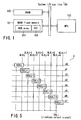
- FIG. 20 is a block diagram showing the configuration of a control system using a conventional NAND flash memory.
- a microprocessor (MPU) 103 is connected to a ROM 104, an SRAM 102 and a NAND flash memory 105 via a system I/O bus line.
- the MPU 103 reads the system boot programs from the ROM 104 when the system starts up, and controls the SRAM 102 and the NAND flash memory 105.
- the system boot programs include codes for making error corrections on data of the NAND flash memory 105.
- the NAND flash memory 105 is used as a file storage in a similar manner as a magnetic disk, and also, is used as an image memory in a digital camera and the like.
- the system using the conventional flash memory requires additional devices such as a controller chip for making error corrections and a ROM for storing boot programs. For this reason, there is a problem that many constituent devices are needed to compose the control system.
- a non-volatile semiconductor memory device comprising:
- an electronic card loaded with the non-volatile semiconductor memory device of the first aspect of the present invention.
- an electronic apparatus comprising:
- FIG. 1 is a block diagram showing the configuration of a NAND flash memory according to a first embodiment of the present invention and a control system using the same.
- the same reference numerals are used to designate elements corresponding to FIG. 20, and the details are omitted.
- a NAND flash memory 101 includes a memory cell array area which is used as a ROM area 201 and another area which is used as an error correction circuit (ECC) area 202 for performing data corrections on data of the ROM area 201.
- ECC error correction circuit
- Access to memory sections other than the ROM area 201 in the NAND flash memory 101 is made using the same interface as the conventional NAND flash memory 105, and thereby, compatibility with the conventional NAND flash memory is kept.
- the MPU 103 makes access to the NAND flash memory 101 via the system I/O bus line 100 in system boot (startup) to read system boot programs including control codes for NAND flash memory 101 and codes for making data error corrections.
- the MPU 103 which is a controller for controlling NAND flash memory 101 and the like, may detect a rise of the system power source to boot the NAND flash memory 101.
- the NAND flash memory 101 may detect a rise of power source to boot the self. Further, if the system boot programs thus read is copied to the SRAM 102 via the system I/O bus line 100, the SRAM 102 is used as cache memory so long as the system power is supplied; therefore, it is convenient.
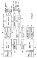
- FIG. 2 is a block diagram showing the configuration of the NAND flash memory 101 shown in FIG. 1.
- the NAND flash memory 101 of the embodiment is provided with several (e.g., two) memory cell arrays 1a and 1b.
- the memory cell arrays 1a and 1b are provided with column control circuits 2a, 2b, row control circuits 3a, 3b, source line control circuit 4a, 4b, and p-well control circuits 5a, 5b, respectively.
- the memory cell arrays 1a and 1b each has a plurality of flash memory cells arrayed in a matrix manner.
- the column control circuits 2a and 2b are arranged adjacent to individually corresponding memory cell arrays 1a and 1b.
- the column control circuits 2a and 2b control bit lines of memory cell arrays 1a and 1b, and make data erase, data write and data read with respect to the selected memory cells.
- the row control circuits 3a and 3b select word lines of individually corresponding memory cell arrays 1a and 1b, and applies voltages required for data erase, data write and data read.
- the source line control circuits 4a and 4b control source lines of individually corresponding memory cell arrays 1a and 1b.
- the p-well control circuits 5a and 5b control the potentials of p-wells formed in the semiconductor substrate with respect to individually corresponding memory cell arrays 1a and 1b.
- a data I/O buffer 6 is connected to an external I/O line D0-D7 to receive write data, output read data and receive address data and command data. More specifically, the data I/O buffer 6 sends write data received from an external device to column control circuits 2a and 2b. Then, the data I/O buffer 6 receives data read from these column control circuits 2a and 2, and thereafter, outputs the read data to the external device. In addition, the data I/O buffer 6 sends address data received from the external device to select the memory cell to column control circuits 2a and 2b and row control circuits 3a and 3b via a state machine 9. In addition, the data I/O buffer 6 sends command data received from the external device to a command interface 7.
- the command interface 7 receives control signals CEn, REn, ALE and CLE from the external device, and determines whether data inputted to the data I/O buffer 6 is write data, command data or address data. If the inputted data is command data, the command interface 7 transfers the command data to the state machine 9 as a receipt command signal.
- An error correction circuit 8 generates check codes for error correction with respect to the write data received from the external device. In addition, the error correction circuit 8 detects an error from data read from memory cells of memory cell arrays 1a and 1b.
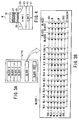
- FIGS. 3A and 3B are diagrams showing the configuration of typical memory cell array 1a, for example, selected from two memory cell arrays 1a and 1b shown in FIG. 1.
- the memory cell array 1a is divided into several blocks BLOCK0-BLOCK1023, as shown in FIG. 3A.
- each NAND type memory unit comprises four memory cells M connected in series.
- the gate of the second select gate transistor SG2 is connected to a second select gate line SGS-i corresponding to the block BLOCKi.
- the gates of four memory cells M are connected individually to word lines WL0-i to WL3-i corresponding to the block BLOCKi. Data write and read are simultaneously carried out with respect to 4224 memory cells connected to one word line.
- One-bit data stored in each memory cell (4224 bits in total, 528-byte data using continuously adjacent 8 bits as one unit) forms write and read minimum unit (page).
- FIG. 4 is a cross-sectional view showing the structure of typical one selected from memory cells M shown in FIG. 3B.
- Double structure of n-well 12 and p-well 13 is formed on a p-type semiconductor substrate 11.
- n-type diffusion layers 14 formed on the p-well 13 function as source/drain regions.
- a tunnel oxide film 15 is formed on a channel region, and a floating gate 16 is stacked thereon.
- ONO film (stacked film comprising Oxide film/Nitride film/Oxide film) 17 and control gate 18 are stacked in the order mentioned.
- the control gate 18 functions as part of the word line.
- FIG. 5 is a circuit diagram showing the configuration of a part (corresponding to one-byte data) of one of the two column control circuits 2a and 2b shown in FIG. 2.
- Data storage circuits (DS) DS8j to DS8j+7 are connected to eight bit lines BL8j to BL8j+7, respectively.
- the data storage circuits DS8j to DS8j+7 are connected to the data I/O buffer 6 shown in FIG. 2 via data I/O lines d0 to d7, and stores write data or read data.
- the data storage circuits are selected by the same column select signal CSLj using eight data storage circuits DS8j to DS8j+7 as a unit, and data is inputted thereto or outputted therefrom.
- the data storage circuits DS8j to DS8j+7 control voltages of bit lines BL8j to BL8j+7 according to stored write data, thereby carrying out write control.
- the data storage circuits DS8j to DS8j+7 sense voltages on the bit lines BL8j to BL8j+7 to store the data.
- the eight data storage circuits DS8j to DS8j+7 are each controlled according to the common control signal CSLj except for the data I/O operation during which these circuits simultaneously function.
- FIG. 6 is a view showing the relationship between data or number of the NAND flash memory shown in FIG. 2 and threshold voltages of the memory cell M shown in FIG. 4 and its distribution.
- Data erase is carried out by applying a high voltage (e.g., 20V) to the p-well 13 of FIG. 4 and setting the control gate 18 to 0V. In this case, electrons are ejected from the floating gate 16 to the p-well 13 via the tunnel oxide film 15, so that the threshold voltage of the memory cell M becomes 0V or less. This is "0" storage state.
- a high voltage e.g. 20V
- Data write is carried out by setting the p-well 13 and the n-type diffusion layers 14 to 0V and setting the control gate 18 to a high voltage (e.g., 20V). By doing so, electrons are injected from the channel region to the floating gate 16, so that the threshold voltage of the memory cell M becomes positive. In this case, if the threshold voltage exceeds 0.8V, the write operation is inhibited every memory cell; therefore, the threshold voltage becomes 4.5V or less. This is "1" write state.
- a high voltage e.g. 20V
- the table 1 shows voltages of each element in erase, write, read, erase verify and write verify operations. Incidentally, in the write and read operations shown in the table 1, it is assumed that one word line (e.g., WL2) of four word lines WL0 to WL3 corresponding to four memory cells M is selected.
- one word line e.g., WL2
- Read is carried out by applying a read voltage of 0V to the selected word line WL2. If the threshold voltage of the selected memory cell M is less than the read voltage, the selected bit line BLj is connected to the common source line C-source. Therefore, the potential of the bit line BLj becomes relatively low level L. On the contrary, if the threshold voltage of the selected memory cell M is more than the read voltage, the selected bit line BLj is not connected to the common source line C-source. Therefore, the potential of the bit line BLj becomes relatively high level H.
- Erase verify is carried out by setting all word lines W10 to WL3 of the selected block to 0V. If the threshold voltages of four memory cells M in the NAND type memory unit are all less than 0V, the bit lines BLj are connected to the common source line C-source. Therefore, the potential of the bit lines BLj becomes relatively low level L. On the contrary, if the threshold voltage of any one of four memory cells M is more than 0V, the path between the bit line BLj and the common source line C-source are non-conductive. Therefore, the potential of the bit line BLj becomes at a relatively high level H.
- Write verify is carried out by applying a verify voltage of 0.8V to the selected word line WL2. If the threshold voltage of the memory cell M is less than the verify voltage, the current path between the bit line BLi and the common source line C-source becomes conductive. Therefore, the potential of the bit line BLi becomes at a relatively low level L. On the contrary, if the threshold voltage of the memory cell M is more than the verify voltage, the current path between the bit line BLi and the common source line C-source are non-conductive. Therefore, the potential of the bit line BLi is held at a relatively high level H.
- FIG. 7 is a view showing a data format in a memory block BLOCKi provided outside of the ROM area in the memory cell arrays 1a and 1b shown in FIG. 2.
- the row address 4i corresponds to the word line equivalent to the word line WL0_i of FIG. 3, that is, to the page Page0, which is a write/read unit.
- the row address 4i+1 corresponds to the page Page1
- the row address 4i+2 corresponds to the page Page2
- the row address 4i+3 corresponds to the page Page3.
- File data is stored in memory cells corresponding to the addresses 0 to 511 of the column addresses 0 to 527 shown in FIG. 7 with a 512-byte data length N.
- the 512-byte data length N corresponds to the sector size of a magnetic disk so that it is convenient when the magnetic disk is replaced with the NAND flash memory.
- the file data is used after being transferred to the SRAM 102 shown in FIG. 2.
- Logical address data of the file data and an error check code are stored in memory cells corresponding to the addresses 512 to 527 in the column addresses 0 to 527 shown in FIG. 7 with 16-byte data length M (N > M).
- the error check code is concerned with the file data and the logical address data.
- the error check code is generated in the MPU 103 of FIG. 1 with respect to the file data and the logical address data, and thereafter, written to the NAND flash memory 101. If an error exists in the file data and the logical address data read from the NAND flash memory 101, the MPU 103 makes corrections using the corresponding error check code.
- FIG. 8A shows a data format using a block BLOCK0a of an ROM area in the memory cell array 1a shown in FIG. 2, and FIG. 8B shows a data format using a block BLOCKOb of another ROM area in the memory cell array 1b.
- the two blocks BLOCK0a and BLOCK0b are used not to store file data such as those stored in a magnetic disk, but to store system boot programs of various electronic apparatuses. For this reason, sufficient amount of data necessary for starting the system should be stored more than that of 528-byte unit data length.
- data longer than the 512-byte data length N is stored as a series of data using two blocks BLOCK0a and BLOCKOb.
- the 1 K-byte data is replaced with the data of the conventional ROM 104 shown in FIG. 20; therefore, it is convenient to use the k-th power of 2 (k is positive integers, K > N) as the data length K.
- the error check code generated by the error correction circuit 8 of FIG. 2 is stored in 16-byte area of the column addresses 512 to 527 of the second page Page0b with respect to the 1 K-byte data.
- blocks BLOCK0a and BLOCK0b of ROM areas of the two memory cell arrays 1a and 1b are used in a state of being combined. By doing so, access is simultaneously made with respect to the blocks BLOCK0a and BLOCK0b of the two ROM areas. Therefore, access can be simply made in the embodiment.
- the NAND flash memory of the embodiment has the following constitutive features.
- the NAND flash memory comprises electrically rewritable non-volatile semiconductor memory cells, an interface (6, 7, 9), an error correction circuit 8, and a control circuit (2a to 5a and 2b to 5b). More specifically, the interface (6, 7, 9) makes data exchange with an external device to carry out data write/read with respect to the non-volatile semiconductor memory cells, and decodes commands.
- the error correction circuit 8 makes error corrections with respect to write data/read data of the non-volatile semiconductor memory' cells.
- the control circuit controls these non-volatile semiconductor memory cells.
- the flash memory itself has the function equivalent to an ROM for booting the system using the same.
- the NAND flash memory has the following functions (details thereof will be described later with reference to FIG. 9A to FIG. 14H).
- the first read mode data is read from the non-volatile semiconductor memory cells via a first bootstrap.
- the second read mode data is read from the non-volatile semiconductor memory cells via a second bootstrap. During the second read mode, part of the signals inputted to the interface is invalidated.
- FIGS. 9A to 9H are timing waveform charts to explain the operation of reading data except for the ROM area of the NAND flash memory shown in FIG. 2 in the same read mode as the conventional NAND flash memory.
- a page is selected, and data is read from the memory cell arrays 1a or 1b to column control circuit 2a or 2b.
- "L" is outputted as a busy signal Busy. If data output to an external device is possible from the column control circuit 2a or 2b via the data I/O buffer 6, the busy signal Busy is returned to "H". Thereafter, data is outputted in synchronous with a read enable signal REn, and when the last data (528-th byte data) of the selected page is outputted, output standby state is automatically given.
- those data denoted by the hatched portions in FIG. 9F show that the denoted data may be undefined.
- FIGS. 10A to 10H are timing waveform charts to explain the operation of reading data except for the ROM area of the NAND memory shown in FIG. 2 in a read mode different from the read mode shown in FIGS. 9A to 9H.
- command standby state coincides with read standby state.
- reset signal RESETn is "H” and the signal ALE is "H"
- data inputted to the data I/O buffer 6 is fetched as address data Add0 to Add3 every when the signal WEn becomes "L”.
- a page is selected, and data is read from the memory cell arrays 1a or 1b to the column control circuit 2a or 2b.
- "L" is outputted as a busy signal Busy. If data output to an external device is possible from column control circuit 2a or 2b via the data I/O buffer 6, the busy signal Busy is returned to "H". Thereafter, data is outputted in synchronous with a read enable signal REn, and when the last data (528-th byte data) of the selected page is outputted, the next page is automatically selected.
- busy state that is, output standby state is given.
- hatched portions in FIG. 10F are those data which may be undefined.
- FIGS. 11A to 11H are timing waveform charts to explain the operation of carrying out system boot (boot operation) in a command-less address mode by hardware reset of the NAND flash memory according to data of the ROM area of the NAND memory shown in FIG. 2.
- Hardware reset is booted when the reset signal RESETn supplied from the system controller becomes "H".
- signals ALE and CLE are invalidated, and pages Page0a and Page0b are selected so that data can be read from the memory cell array 1a or 1b to the column control circuit 2a or 2b.
- "L" is outputted as the busy signal Busy. If data output to an external device is possible from the column control circuit 2a or 2b via the data I/O buffer 6, the busy signal Busy is restored to "H".
- the error correction circuit 8 detects an error position from data read to the column control circuit 2a or 2b while "L" is outputting as the busy signal Busy. By doing so, data having an error is outputted after being inverted in the output operation.
- data denoted by the hatched portions in FIGS. 11A to 11H are data which may be undefined.
- tRCV denotes a recovery period, and the recovery operation is carried out from the fall of the signal WEn until boot mode is completed.
- one or more signals (signals ALE, CLE in the embodiment) of whole signals inputted to the interface is invalidated.
- the reset signal RESETn may be automatically generated by an internal circuit of the electronic apparatus.
- the NAND flash memory 101 is provided with a power supply voltage detection circuit 10.
- the power supply voltage detection circuit 10 detects a rise of power supply made via a power supply terminal 11 of the NAND flash memory 101.
- a reset signal RESETn is generated after a rise of the power supply is detected.
- the power voltage supplied across the power supply terminal 11 and a ground terminal 12 is applied in common to SRAM 102 and MPU 103.
- FIGS. 12A to 12H are timing waveform charts to explain the operation of carrying out system boot (boot operation) according to a command from MPU 103 by software reset of the NAND flash memory according to the data of the ROM area of the NAND memory shown in FIG. 2.
- the error correction circuit 8 detects an error position from data read to column control circuit 2a or 2b while "L" is outputting as the busy signal Busy. By doing so, data having an error is outputted after being inverted in the output operation. Incidentally, the hatched portions in FIGS. 12A to 12H show that the corresponding data may be undefined.
- FIGS. 13A to 13H are timing waveform charts to explain the operation of writing data to areas other than ROM area of the NAND memory shown in FIG. 2 in the same write mode as the NAND flash memory.
- FIGS. 14A to 14H are timing waveform charts to explain the operation of writing data to the ROM area of the NAND memory shown in FIG. 2.
- FIG. 15 shows an electronic card using the NAND flash memory of the above-mentioned embodiment and an electronic apparatus using the electronic card.
- a portable (mobile) electronic apparatus that is, a digital still camera 50 given as one example of the electronic apparatus.
- An electronic card (e.g., memory card) 51 used as recoding medium of the digital still camera 50 has a built-in IC package PK1, which is integrated and sealed with the NAND flash memory described in the first embodiment.
- the case of the digital still camera 50 is provided with a card slot 52 and a circuit board (not shown) connected thereto.
- the memory card 51 is electrically connected to electronic circuits on the circuit board in a state of being removably loaded in the card slot 52. If the memory card 51 is a non-contact type IC card, the memory card 51 may be inserted into the card slot 52, or put near the outside of the card slot 52. By doing so, the memory card 51 may be electrically connected to the circuit board by a wireless manner.
- a reference numeral 53 denotes a lens
- 108 denotes a display (e.g., liquid-crystal monitor)
- 112 denotes an operation button (e.g., shutter button)
- 118 denotes a flash lamp.
- FIG. 16 is a block diagram showing the basic configuration of the digital still camera shown in FIG. 15.
- the image pickup device 54 photoelectrically converts the inputted light, and thereafter, outputs an analog signal.
- the analog signal is amplified by an analog amplifier (AMP) included in an analog/digital (A/D) converter 54A, and thereafter, converted into a digital signal by the A/D converter 54A.
- AMP analog amplifier
- A/D converter 54A analog/digital converter 54A
- the converted signal is inputted to a camera signal processing circuit 55.
- the signal is converted into luminance signal and color difference signal after automatic exposure control, automatic white balance control and color separation processing are carried out.
- the signal outputted from the camera signal processing circuit 55 is inputted to a video signal processing circuit 106 so that it can be converted into a video signal.
- a video signal processing circuit 106 For example, NTSC (National Television System Committee) is given as the video signal system.
- a microcomputer 111 controls the image pickup device 54, the A/D converter 54A and camera signal processing circuit 55.
- the video signal is outputted to a display 108 mounted to the housing of the digital still camera 50, which is connected with a display signal processing circuit 107.
- the video signal is supplied to a video output terminal 110 via video driver 109.
- the image picked-up by the digital still camera 50 is outputted as video output to an image display device such as a television set via the video output terminal 110.
- an image display device such as a television set via the video output terminal 110.
- the microcomputer 111 controls a memory controller 113 so that the signal outputted from the camera signal processing circuit 55 can be written to a video memory 114 as a frame image.
- a compressing/expanding circuit 115 compresses the frame image thus written based on a predetermined compression format. Thereafter, the frame image thus compressed is recorded to the memory card 51 loaded in the card slot 52 via a card interface 116.
- the image data recorded to the memory card 51 is read via the card interface 116, and expanded by the compressing/expanding circuit 115, and thereafter, written to the video memory 114.
- the image data thus written is inputted to the video signal processing circuit 106, and the image is displayed on the display 108 or image device like the case of monitoring the image.
- the following components are mounted on the circuit board 100.
- the components are card slot 52, image pickup device 54, A/D converter 54A, camera signal processing circuit 55, video signal processing circuit 106 and display 107. Further, the components are video driver 109, microcomputer 111, memory controller 113, video memory 114, compressing/expanding circuit 115 and card interface 116.
- the card slot 52 does not need to be mounted on the circuit board 100, and may be connected to the circuit board 100 via a connector cable (not shown).
- a power circuit 117 is further mounted on the circuit board 100.
- the power circuit 117 e.g., DC/DC converter
- the internal power supply voltage is supplied to flash lamp 118 and display 108 in addition to the above-mentioned circuits.
- the electronic card 51 of the embodiment is applicable to various apparatuses briefly shown in FIG. 17A to FIG. 17J, in addition to portable electronic device such as the digital still camera. More specifically, FIGS. 17A to FIG. 17J show video camera, television, audio device, game device, electronic music instrument, mobile phone, personal computer, personal digital assistant (PDA), voice recorder and PC card, respectively.
- the PC card shown in FIG. 17J is conformable to the PCMCIA standards such as a PC card memory.
- the non-volatile semiconductor memory device of the present invention is not limited to the NAND type flash memory, and may be applied to NOR type flash memory.
- one aspect of the present invention can provide a non-volatile semiconductor memory device, which has a ROM area capable of storing boot data of the system provided with the memory device, reduces the number of constituent devices of the system, and realizes the system at low cost.
- another aspect of the present invention can provide an electronic card using the non-volatile semiconductor memory device and an electronic apparatus using the electronic card.
Landscapes
- Engineering & Computer Science (AREA)
- Microelectronics & Electronic Packaging (AREA)
- Computer Hardware Design (AREA)
- Physics & Mathematics (AREA)
- General Physics & Mathematics (AREA)
- Theoretical Computer Science (AREA)
- Read Only Memory (AREA)
- Techniques For Improving Reliability Of Storages (AREA)
- Memory System (AREA)
- Semiconductor Memories (AREA)
- Non-Volatile Memory (AREA)
Applications Claiming Priority (2)
| Application Number | Priority Date | Filing Date | Title |
|---|---|---|---|
| JP2003114762 | 2003-04-18 | ||
| JP2003114762A JP4314057B2 (ja) | 2003-04-18 | 2003-04-18 | 不揮発性半導体記憶装置および電子装置 |
Publications (3)
| Publication Number | Publication Date |
|---|---|
| EP1469480A2 true EP1469480A2 (de) | 2004-10-20 |
| EP1469480A3 EP1469480A3 (de) | 2007-04-04 |
| EP1469480B1 EP1469480B1 (de) | 2009-08-05 |
Family
ID=32906102
Family Applications (1)
| Application Number | Title | Priority Date | Filing Date |
|---|---|---|---|
| EP04008974A Expired - Lifetime EP1469480B1 (de) | 2003-04-18 | 2004-04-15 | Nichtflüchtige Halbleiterspeicheranordnung, diese verwendende elektronische Karte und elektronische Vorrichtung |
Country Status (7)
| Country | Link |
|---|---|
| US (2) | US6990018B2 (de) |
| EP (1) | EP1469480B1 (de) |
| JP (1) | JP4314057B2 (de) |
| KR (1) | KR100599905B1 (de) |
| CN (1) | CN100530413C (de) |
| DE (1) | DE602004022353D1 (de) |
| TW (1) | TWI237270B (de) |
Cited By (2)
| Publication number | Priority date | Publication date | Assignee | Title |
|---|---|---|---|---|
| WO2007136704A3 (en) * | 2006-05-18 | 2008-03-06 | Micron Technology Inc | Nand system with a data write frequency greater than a command-and-address-load frequency |
| EP2158564A4 (de) * | 2007-06-21 | 2010-08-04 | Toshiba Kk | Speicherungsvorrichtung, elektronische vorrichtung und host-vorrichtung |
Families Citing this family (39)
| Publication number | Priority date | Publication date | Assignee | Title |
|---|---|---|---|---|
| US6985388B2 (en) * | 2001-09-17 | 2006-01-10 | Sandisk Corporation | Dynamic column block selection |
| US7170802B2 (en) * | 2003-12-31 | 2007-01-30 | Sandisk Corporation | Flexible and area efficient column redundancy for non-volatile memories |
| JP4314057B2 (ja) * | 2003-04-18 | 2009-08-12 | サンディスク コーポレイション | 不揮発性半導体記憶装置および電子装置 |
| US7257703B2 (en) * | 2003-11-18 | 2007-08-14 | Toshiba America Electronic Components, Inc. | Bootable NAND flash memory architecture |
| US7401258B1 (en) * | 2004-09-30 | 2008-07-15 | Xilinx, Inc. | Circuit for and method of accessing instruction data written to a memory |
| US7243856B2 (en) * | 2005-03-24 | 2007-07-17 | Sandisk Il Ltd.. | Loading internal applications on a smartcard |
| US7379330B2 (en) * | 2005-11-08 | 2008-05-27 | Sandisk Corporation | Retargetable memory cell redundancy methods |
| JP5192388B2 (ja) * | 2005-11-22 | 2013-05-08 | サンディスク テクノロジィース インコーポレイテッド | レガシーホストのための方法およびメモリシステム |
| US7849302B2 (en) * | 2006-04-10 | 2010-12-07 | Apple Inc. | Direct boot arrangement using a NAND flash memory |
| JP2008134736A (ja) * | 2006-11-27 | 2008-06-12 | Fujifilm Corp | 電子機器 |
| JP4277901B2 (ja) * | 2006-12-27 | 2009-06-10 | ソニー株式会社 | メモリカード、撮像装置及び記録再生装置 |
| JP2009146499A (ja) * | 2007-12-13 | 2009-07-02 | Toshiba Corp | 不揮発性メモリカード |
| JP2010123201A (ja) * | 2008-11-20 | 2010-06-03 | Toshiba Corp | 不揮発性半導体記憶装置 |
| US20100220514A1 (en) * | 2009-03-02 | 2010-09-02 | Lyric Semiconductor, Inc. | Storage devices with soft processing |
| US8458114B2 (en) * | 2009-03-02 | 2013-06-04 | Analog Devices, Inc. | Analog computation using numerical representations with uncertainty |
| US8107306B2 (en) | 2009-03-27 | 2012-01-31 | Analog Devices, Inc. | Storage devices with soft processing |
| JP5266589B2 (ja) * | 2009-05-14 | 2013-08-21 | ルネサスエレクトロニクス株式会社 | 不揮発性半導体記憶装置 |
| US8102705B2 (en) * | 2009-06-05 | 2012-01-24 | Sandisk Technologies Inc. | Structure and method for shuffling data within non-volatile memory devices |
| US8027195B2 (en) * | 2009-06-05 | 2011-09-27 | SanDisk Technologies, Inc. | Folding data stored in binary format into multi-state format within non-volatile memory devices |
| US7974124B2 (en) * | 2009-06-24 | 2011-07-05 | Sandisk Corporation | Pointer based column selection techniques in non-volatile memories |
| US20110002169A1 (en) | 2009-07-06 | 2011-01-06 | Yan Li | Bad Column Management with Bit Information in Non-Volatile Memory Systems |
| US8144512B2 (en) | 2009-12-18 | 2012-03-27 | Sandisk Technologies Inc. | Data transfer flows for on-chip folding |
| US8468294B2 (en) * | 2009-12-18 | 2013-06-18 | Sandisk Technologies Inc. | Non-volatile memory with multi-gear control using on-chip folding of data |
| US8725935B2 (en) | 2009-12-18 | 2014-05-13 | Sandisk Technologies Inc. | Balanced performance for on-chip folding of non-volatile memories |
| JP5269020B2 (ja) | 2010-09-22 | 2013-08-21 | 株式会社東芝 | 半導体集積回路装置およびメモリの管理方法 |
| KR101692432B1 (ko) * | 2010-12-23 | 2017-01-17 | 삼성전자주식회사 | 불 휘발성 메모리 장치 |
| US9342446B2 (en) | 2011-03-29 | 2016-05-17 | SanDisk Technologies, Inc. | Non-volatile memory system allowing reverse eviction of data updates to non-volatile binary cache |
| CN103000216B (zh) * | 2011-09-15 | 2015-06-24 | 华邦电子股份有限公司 | 读出装置 |
| US8472261B2 (en) * | 2011-10-17 | 2013-06-25 | Winbond Electronics Corp. | Reading devices for memory arrays |
| US8842473B2 (en) | 2012-03-15 | 2014-09-23 | Sandisk Technologies Inc. | Techniques for accessing column selecting shift register with skipped entries in non-volatile memories |
| US8681548B2 (en) | 2012-05-03 | 2014-03-25 | Sandisk Technologies Inc. | Column redundancy circuitry for non-volatile memory |
| US8897080B2 (en) | 2012-09-28 | 2014-11-25 | Sandisk Technologies Inc. | Variable rate serial to parallel shift register |
| US9076506B2 (en) | 2012-09-28 | 2015-07-07 | Sandisk Technologies Inc. | Variable rate parallel to serial shift register |
| US9490035B2 (en) | 2012-09-28 | 2016-11-08 | SanDisk Technologies, Inc. | Centralized variable rate serializer and deserializer for bad column management |
| US9934872B2 (en) | 2014-10-30 | 2018-04-03 | Sandisk Technologies Llc | Erase stress and delta erase loop count methods for various fail modes in non-volatile memory |
| US9224502B1 (en) | 2015-01-14 | 2015-12-29 | Sandisk Technologies Inc. | Techniques for detection and treating memory hole to local interconnect marginality defects |
| US10032524B2 (en) | 2015-02-09 | 2018-07-24 | Sandisk Technologies Llc | Techniques for determining local interconnect defects |
| US9564219B2 (en) | 2015-04-08 | 2017-02-07 | Sandisk Technologies Llc | Current based detection and recording of memory hole-interconnect spacing defects |
| US9269446B1 (en) | 2015-04-08 | 2016-02-23 | Sandisk Technologies Inc. | Methods to improve programming of slow cells |
Citations (3)
| Publication number | Priority date | Publication date | Assignee | Title |
|---|---|---|---|---|
| JP2001014888A (ja) | 1999-06-28 | 2001-01-19 | Toshiba Corp | フラッシュメモリ |
| US20020021595A1 (en) | 2000-05-30 | 2002-02-21 | Keiji Terada | Boot block flash memory control circuit; IC memory card and semiconductor memory device incorporating the same; and erasure method for boot block flash memory |
| JP3272903B2 (ja) | 1995-03-16 | 2002-04-08 | 株式会社東芝 | 誤り訂正検出回路と半導体記憶装置 |
Family Cites Families (8)
| Publication number | Priority date | Publication date | Assignee | Title |
|---|---|---|---|---|
| US566371A (en) * | 1896-08-25 | Island | ||
| JP3999822B2 (ja) * | 1993-12-28 | 2007-10-31 | 株式会社東芝 | 記憶システム |
| US5603001A (en) * | 1994-05-09 | 1997-02-11 | Kabushiki Kaisha Toshiba | Semiconductor disk system having a plurality of flash memories |
| JPH09288895A (ja) * | 1996-04-19 | 1997-11-04 | Toshiba Corp | 3値記憶半導体記憶システム |
| JPH11203860A (ja) * | 1998-01-07 | 1999-07-30 | Nec Corp | 半導体記憶装置 |
| US6469955B1 (en) * | 2000-11-21 | 2002-10-22 | Integrated Memory Technologies, Inc. | Integrated circuit memory device having interleaved read and program capabilities and methods of operating same |
| JP3815936B2 (ja) * | 2000-01-25 | 2006-08-30 | 株式会社ルネサステクノロジ | Icカード |
| JP4314057B2 (ja) * | 2003-04-18 | 2009-08-12 | サンディスク コーポレイション | 不揮発性半導体記憶装置および電子装置 |
-
2003
- 2003-04-18 JP JP2003114762A patent/JP4314057B2/ja not_active Expired - Lifetime
-
2004
- 2004-04-14 US US10/823,737 patent/US6990018B2/en not_active Expired - Lifetime
- 2004-04-14 KR KR1020040025773A patent/KR100599905B1/ko not_active Expired - Fee Related
- 2004-04-15 EP EP04008974A patent/EP1469480B1/de not_active Expired - Lifetime
- 2004-04-15 DE DE602004022353T patent/DE602004022353D1/de not_active Expired - Lifetime
- 2004-04-15 TW TW093110558A patent/TWI237270B/zh not_active IP Right Cessation
- 2004-04-16 CN CNB2004100329250A patent/CN100530413C/zh not_active Expired - Lifetime
-
2005
- 2005-11-30 US US11/289,509 patent/US7394704B2/en not_active Expired - Lifetime
Patent Citations (3)
| Publication number | Priority date | Publication date | Assignee | Title |
|---|---|---|---|---|
| JP3272903B2 (ja) | 1995-03-16 | 2002-04-08 | 株式会社東芝 | 誤り訂正検出回路と半導体記憶装置 |
| JP2001014888A (ja) | 1999-06-28 | 2001-01-19 | Toshiba Corp | フラッシュメモリ |
| US20020021595A1 (en) | 2000-05-30 | 2002-02-21 | Keiji Terada | Boot block flash memory control circuit; IC memory card and semiconductor memory device incorporating the same; and erasure method for boot block flash memory |
Non-Patent Citations (1)
| Title |
|---|
| T. TANZAWA ET AL.: "A Compact On-chip ECC for Low Cost Flash Memories", SYMPOSIUM ON VLSI CIRCUITS DIGEST OF TECHNICAL PAPERS, 1996 |
Cited By (5)
| Publication number | Priority date | Publication date | Assignee | Title |
|---|---|---|---|---|
| WO2007136704A3 (en) * | 2006-05-18 | 2008-03-06 | Micron Technology Inc | Nand system with a data write frequency greater than a command-and-address-load frequency |
| US7558131B2 (en) | 2006-05-18 | 2009-07-07 | Micron Technology, Inc. | NAND system with a data write frequency greater than a command-and-address-load frequency |
| US7855927B2 (en) | 2006-05-18 | 2010-12-21 | Micron Technology, Inc. | NAND system with a data write frequency greater than a command-and-address-load frequency |
| EP2158564A4 (de) * | 2007-06-21 | 2010-08-04 | Toshiba Kk | Speicherungsvorrichtung, elektronische vorrichtung und host-vorrichtung |
| CN101689246B (zh) * | 2007-06-21 | 2012-05-09 | 株式会社东芝 | 存储器装置、电子装置以及主机设备 |
Also Published As
| Publication number | Publication date |
|---|---|
| JP4314057B2 (ja) | 2009-08-12 |
| US20060077712A1 (en) | 2006-04-13 |
| JP2004319048A (ja) | 2004-11-11 |
| CN100530413C (zh) | 2009-08-19 |
| TWI237270B (en) | 2005-08-01 |
| DE602004022353D1 (de) | 2009-09-17 |
| US6990018B2 (en) | 2006-01-24 |
| EP1469480B1 (de) | 2009-08-05 |
| EP1469480A3 (de) | 2007-04-04 |
| KR20040090713A (ko) | 2004-10-26 |
| TW200425147A (en) | 2004-11-16 |
| CN1538449A (zh) | 2004-10-20 |
| KR100599905B1 (ko) | 2006-07-19 |
| US7394704B2 (en) | 2008-07-01 |
| US20040257874A1 (en) | 2004-12-23 |
Similar Documents
| Publication | Publication Date | Title |
|---|---|---|
| US7394704B2 (en) | Non-volatile semiconductor memory device, electronic card using the same and electronic apparatus | |
| US7502258B2 (en) | Semiconductor memory device | |
| CN101101792B (zh) | 半导体存储装置 | |
| KR100690476B1 (ko) | 불휘발성 반도체 기억 장치 | |
| US7349249B2 (en) | Semiconductor memory device | |
| KR100585363B1 (ko) | 불휘발성 반도체 기억 장치 | |
| US8111551B2 (en) | Nonvolatile semiconductor memory device having protection function for each memory block | |
| JP4287222B2 (ja) | 不揮発性半導体記憶装置 | |
| KR100624590B1 (ko) | 불휘발성 반도체 기억 장치 | |
| US20060245259A1 (en) | Semiconductor memory device | |
| US7460427B2 (en) | Semiconductor integrated circuit device | |
| JP2004326974A (ja) | 半導体集積回路装置及びicカード | |
| US20090279365A1 (en) | Non-volatile semiconductor memory system | |
| JP2005285184A (ja) | 不揮発性半導体記憶装置 |
Legal Events
| Date | Code | Title | Description |
|---|---|---|---|
| PUAI | Public reference made under article 153(3) epc to a published international application that has entered the european phase |
Free format text: ORIGINAL CODE: 0009012 |
|
| 17P | Request for examination filed |
Effective date: 20040415 |
|
| AK | Designated contracting states |
Kind code of ref document: A2 Designated state(s): AT BE BG CH CY CZ DE DK EE ES FI FR GB GR HU IE IT LI LU MC NL PL PT RO SE SI SK TR |
|
| AX | Request for extension of the european patent |
Extension state: AL HR LT LV MK |
|
| PUAL | Search report despatched |
Free format text: ORIGINAL CODE: 0009013 |
|
| AK | Designated contracting states |
Kind code of ref document: A3 Designated state(s): AT BE BG CH CY CZ DE DK EE ES FI FR GB GR HU IE IT LI LU MC NL PL PT RO SE SI SK TR |
|
| AX | Request for extension of the european patent |
Extension state: AL HR LT LV MK |
|
| 17Q | First examination report despatched |
Effective date: 20070831 |
|
| AKX | Designation fees paid |
Designated state(s): DE FR GB |
|
| GRAP | Despatch of communication of intention to grant a patent |
Free format text: ORIGINAL CODE: EPIDOSNIGR1 |
|
| GRAS | Grant fee paid |
Free format text: ORIGINAL CODE: EPIDOSNIGR3 |
|
| GRAA | (expected) grant |
Free format text: ORIGINAL CODE: 0009210 |
|
| AK | Designated contracting states |
Kind code of ref document: B1 Designated state(s): DE FR GB |
|
| REG | Reference to a national code |
Ref country code: GB Ref legal event code: FG4D |
|
| REF | Corresponds to: |
Ref document number: 602004022353 Country of ref document: DE Date of ref document: 20090917 Kind code of ref document: P |
|
| PLBE | No opposition filed within time limit |
Free format text: ORIGINAL CODE: 0009261 |
|
| STAA | Information on the status of an ep patent application or granted ep patent |
Free format text: STATUS: NO OPPOSITION FILED WITHIN TIME LIMIT |
|
| 26N | No opposition filed |
Effective date: 20100507 |
|
| REG | Reference to a national code |
Ref country code: FR Ref legal event code: PLFP Year of fee payment: 13 |
|
| REG | Reference to a national code |
Ref country code: DE Ref legal event code: R081 Ref document number: 602004022353 Country of ref document: DE Owner name: KIOXIA CORPORATION, JP Free format text: FORMER OWNERS: KABUSHIKI KAISHA TOSHIBA, TOKYO, JP; SANDISK CORP., SUNNYVALE, CALIF., US Ref country code: DE Ref legal event code: R082 Ref document number: 602004022353 Country of ref document: DE Representative=s name: HOFFMANN - EITLE PATENT- UND RECHTSANWAELTE PA, DE Ref country code: DE Ref legal event code: R081 Ref document number: 602004022353 Country of ref document: DE Owner name: KABUSHIKI KAISHA TOSHIBA, JP Free format text: FORMER OWNERS: KABUSHIKI KAISHA TOSHIBA, TOKYO, JP; SANDISK CORP., SUNNYVALE, CALIF., US Ref country code: DE Ref legal event code: R081 Ref document number: 602004022353 Country of ref document: DE Owner name: SANDISK TECHNOLOGIES LLC, PLANO, US Free format text: FORMER OWNERS: KABUSHIKI KAISHA TOSHIBA, TOKYO, JP; SANDISK CORP., SUNNYVALE, CALIF., US Ref country code: DE Ref legal event code: R081 Ref document number: 602004022353 Country of ref document: DE Owner name: TOSHIBA MEMORY CORPORATION, JP Free format text: FORMER OWNERS: KABUSHIKI KAISHA TOSHIBA, TOKYO, JP; SANDISK CORP., SUNNYVALE, CALIF., US |
|
| REG | Reference to a national code |
Ref country code: FR Ref legal event code: TQ Owner name: KABUSHIKI KAISHA TOSHIBA, JP Effective date: 20161222 Ref country code: FR Ref legal event code: TQ Owner name: SANDISK TECHNOLOGIES LLC, US Effective date: 20161222 |
|
| REG | Reference to a national code |
Ref country code: FR Ref legal event code: PLFP Year of fee payment: 14 |
|
| REG | Reference to a national code |
Ref country code: GB Ref legal event code: 732E Free format text: REGISTERED BETWEEN 20170316 AND 20170323 |
|
| REG | Reference to a national code |
Ref country code: FR Ref legal event code: PLFP Year of fee payment: 15 |
|
| REG | Reference to a national code |
Ref country code: DE Ref legal event code: R081 Ref document number: 602004022353 Country of ref document: DE Owner name: KIOXIA CORPORATION, JP Free format text: FORMER OWNERS: KABUSHIKI KAISHA TOSHIBA, TOKIO/TOKYO, JP; SANDISK TECHNOLOGIES LLC, PLANO, TEX., US Ref country code: DE Ref legal event code: R082 Ref document number: 602004022353 Country of ref document: DE Representative=s name: HOFFMANN - EITLE PATENT- UND RECHTSANWAELTE PA, DE Ref country code: DE Ref legal event code: R081 Ref document number: 602004022353 Country of ref document: DE Owner name: SANDISK TECHNOLOGIES LLC, PLANO, US Free format text: FORMER OWNERS: KABUSHIKI KAISHA TOSHIBA, TOKIO/TOKYO, JP; SANDISK TECHNOLOGIES LLC, PLANO, TEX., US Ref country code: DE Ref legal event code: R081 Ref document number: 602004022353 Country of ref document: DE Owner name: TOSHIBA MEMORY CORPORATION, JP Free format text: FORMER OWNERS: KABUSHIKI KAISHA TOSHIBA, TOKIO/TOKYO, JP; SANDISK TECHNOLOGIES LLC, PLANO, TEX., US |
|
| REG | Reference to a national code |
Ref country code: FR Ref legal event code: TQ Owner name: TOSHIBA MEMORY CORPORATION, JP Effective date: 20181031 Ref country code: FR Ref legal event code: TQ Owner name: SANDISK TECHNOLOGIES LLC, US Effective date: 20181031 |
|
| REG | Reference to a national code |
Ref country code: GB Ref legal event code: 732E Free format text: REGISTERED BETWEEN 20190321 AND 20190327 |
|
| PGFP | Annual fee paid to national office [announced via postgrant information from national office to epo] |
Ref country code: FR Payment date: 20210309 Year of fee payment: 18 |
|
| PGFP | Annual fee paid to national office [announced via postgrant information from national office to epo] |
Ref country code: GB Payment date: 20210324 Year of fee payment: 18 |
|
| REG | Reference to a national code |
Ref country code: DE Ref legal event code: R081 Ref document number: 602004022353 Country of ref document: DE Owner name: SANDISK TECHNOLOGIES LLC, PLANO, US Free format text: FORMER OWNERS: SANDISK TECHNOLOGIES LLC, PLANO, TEX., US; TOSHIBA MEMORY CORPORATION, TOKYO, JP Ref country code: DE Ref legal event code: R081 Ref document number: 602004022353 Country of ref document: DE Owner name: KIOXIA CORPORATION, JP Free format text: FORMER OWNERS: SANDISK TECHNOLOGIES LLC, PLANO, TEX., US; TOSHIBA MEMORY CORPORATION, TOKYO, JP |
|
| REG | Reference to a national code |
Ref country code: GB Ref legal event code: 732E Free format text: REGISTERED BETWEEN 20220127 AND 20220202 |
|
| GBPC | Gb: european patent ceased through non-payment of renewal fee |
Effective date: 20220415 |
|
| PG25 | Lapsed in a contracting state [announced via postgrant information from national office to epo] |
Ref country code: GB Free format text: LAPSE BECAUSE OF NON-PAYMENT OF DUE FEES Effective date: 20220415 Ref country code: FR Free format text: LAPSE BECAUSE OF NON-PAYMENT OF DUE FEES Effective date: 20220430 |
|
| PGFP | Annual fee paid to national office [announced via postgrant information from national office to epo] |
Ref country code: DE Payment date: 20230228 Year of fee payment: 20 |
|
| REG | Reference to a national code |
Ref country code: DE Ref legal event code: R071 Ref document number: 602004022353 Country of ref document: DE |