EP1465147A2 - Drive circuit for display apparatus with selective inactivation of amplifier units for reducing power consumption - Google Patents
Drive circuit for display apparatus with selective inactivation of amplifier units for reducing power consumption Download PDFInfo
- Publication number
- EP1465147A2 EP1465147A2 EP04005117A EP04005117A EP1465147A2 EP 1465147 A2 EP1465147 A2 EP 1465147A2 EP 04005117 A EP04005117 A EP 04005117A EP 04005117 A EP04005117 A EP 04005117A EP 1465147 A2 EP1465147 A2 EP 1465147A2
- Authority
- EP
- European Patent Office
- Prior art keywords
- gradation
- circuit
- data
- lines
- image data
- Prior art date
- Legal status (The legal status is an assumption and is not a legal conclusion. Google has not performed a legal analysis and makes no representation as to the accuracy of the status listed.)
- Withdrawn
Links
- 230000002779 inactivation Effects 0.000 title 1
- 230000004044 response Effects 0.000 claims abstract description 42
- 238000000034 method Methods 0.000 claims description 16
- 239000011159 matrix material Substances 0.000 claims description 3
- 230000003213 activating effect Effects 0.000 claims 2
- 238000010586 diagram Methods 0.000 description 29
- 239000004973 liquid crystal related substance Substances 0.000 description 14
- 230000006870 function Effects 0.000 description 11
- 239000000872 buffer Substances 0.000 description 8
- 230000010355 oscillation Effects 0.000 description 6
- 230000008859 change Effects 0.000 description 5
- 238000006243 chemical reaction Methods 0.000 description 5
- 230000008569 process Effects 0.000 description 5
- 230000009467 reduction Effects 0.000 description 5
- 101000885321 Homo sapiens Serine/threonine-protein kinase DCLK1 Proteins 0.000 description 4
- 102100039758 Serine/threonine-protein kinase DCLK1 Human genes 0.000 description 4
- 239000003990 capacitor Substances 0.000 description 3
- 238000005070 sampling Methods 0.000 description 3
- 239000000758 substrate Substances 0.000 description 3
- 238000011144 upstream manufacturing Methods 0.000 description 3
- 102100039216 Dolichyl-diphosphooligosaccharide-protein glycosyltransferase subunit 2 Human genes 0.000 description 2
- 101000670093 Homo sapiens Dolichyl-diphosphooligosaccharide-protein glycosyltransferase subunit 2 Proteins 0.000 description 2
- 230000001360 synchronised effect Effects 0.000 description 2
- 230000015556 catabolic process Effects 0.000 description 1
- 238000007796 conventional method Methods 0.000 description 1
- 238000006731 degradation reaction Methods 0.000 description 1
- 239000011521 glass Substances 0.000 description 1
- 230000007257 malfunction Effects 0.000 description 1
- 230000006386 memory function Effects 0.000 description 1
- 230000002265 prevention Effects 0.000 description 1
- 230000000630 rising effect Effects 0.000 description 1
- 239000004065 semiconductor Substances 0.000 description 1
- 239000000126 substance Substances 0.000 description 1
- 230000001052 transient effect Effects 0.000 description 1
Images










Classifications
-
- G—PHYSICS
- G09—EDUCATION; CRYPTOGRAPHY; DISPLAY; ADVERTISING; SEALS
- G09G—ARRANGEMENTS OR CIRCUITS FOR CONTROL OF INDICATING DEVICES USING STATIC MEANS TO PRESENT VARIABLE INFORMATION
- G09G3/00—Control arrangements or circuits, of interest only in connection with visual indicators other than cathode-ray tubes
- G09G3/20—Control arrangements or circuits, of interest only in connection with visual indicators other than cathode-ray tubes for presentation of an assembly of a number of characters, e.g. a page, by composing the assembly by combination of individual elements arranged in a matrix no fixed position being assigned to or needed to be assigned to the individual characters or partial characters
- G09G3/34—Control arrangements or circuits, of interest only in connection with visual indicators other than cathode-ray tubes for presentation of an assembly of a number of characters, e.g. a page, by composing the assembly by combination of individual elements arranged in a matrix no fixed position being assigned to or needed to be assigned to the individual characters or partial characters by control of light from an independent source
- G09G3/36—Control arrangements or circuits, of interest only in connection with visual indicators other than cathode-ray tubes for presentation of an assembly of a number of characters, e.g. a page, by composing the assembly by combination of individual elements arranged in a matrix no fixed position being assigned to or needed to be assigned to the individual characters or partial characters by control of light from an independent source using liquid crystals
- G09G3/3611—Control of matrices with row and column drivers
- G09G3/3685—Details of drivers for data electrodes
- G09G3/3688—Details of drivers for data electrodes suitable for active matrices only
-
- A—HUMAN NECESSITIES
- A61—MEDICAL OR VETERINARY SCIENCE; HYGIENE
- A61H—PHYSICAL THERAPY APPARATUS, e.g. DEVICES FOR LOCATING OR STIMULATING REFLEX POINTS IN THE BODY; ARTIFICIAL RESPIRATION; MASSAGE; BATHING DEVICES FOR SPECIAL THERAPEUTIC OR HYGIENIC PURPOSES OR SPECIFIC PARTS OF THE BODY
- A61H23/00—Percussion or vibration massage, e.g. using supersonic vibration; Suction-vibration massage; Massage with moving diaphragms
- A61H23/02—Percussion or vibration massage, e.g. using supersonic vibration; Suction-vibration massage; Massage with moving diaphragms with electric or magnetic drive
- A61H23/0218—Percussion or vibration massage, e.g. using supersonic vibration; Suction-vibration massage; Massage with moving diaphragms with electric or magnetic drive with alternating magnetic fields producing a translating or oscillating movement
-
- A—HUMAN NECESSITIES
- A61—MEDICAL OR VETERINARY SCIENCE; HYGIENE
- A61H—PHYSICAL THERAPY APPARATUS, e.g. DEVICES FOR LOCATING OR STIMULATING REFLEX POINTS IN THE BODY; ARTIFICIAL RESPIRATION; MASSAGE; BATHING DEVICES FOR SPECIAL THERAPEUTIC OR HYGIENIC PURPOSES OR SPECIFIC PARTS OF THE BODY
- A61H23/00—Percussion or vibration massage, e.g. using supersonic vibration; Suction-vibration massage; Massage with moving diaphragms
- A61H23/006—Percussion or tapping massage
-
- A—HUMAN NECESSITIES
- A61—MEDICAL OR VETERINARY SCIENCE; HYGIENE
- A61H—PHYSICAL THERAPY APPARATUS, e.g. DEVICES FOR LOCATING OR STIMULATING REFLEX POINTS IN THE BODY; ARTIFICIAL RESPIRATION; MASSAGE; BATHING DEVICES FOR SPECIAL THERAPEUTIC OR HYGIENIC PURPOSES OR SPECIFIC PARTS OF THE BODY
- A61H39/00—Devices for locating or stimulating specific reflex points of the body for physical therapy, e.g. acupuncture
- A61H39/007—Stimulation by mechanical vibrations, e.g. ultrasonic
-
- G—PHYSICS
- G09—EDUCATION; CRYPTOGRAPHY; DISPLAY; ADVERTISING; SEALS
- G09G—ARRANGEMENTS OR CIRCUITS FOR CONTROL OF INDICATING DEVICES USING STATIC MEANS TO PRESENT VARIABLE INFORMATION
- G09G3/00—Control arrangements or circuits, of interest only in connection with visual indicators other than cathode-ray tubes
- G09G3/20—Control arrangements or circuits, of interest only in connection with visual indicators other than cathode-ray tubes for presentation of an assembly of a number of characters, e.g. a page, by composing the assembly by combination of individual elements arranged in a matrix no fixed position being assigned to or needed to be assigned to the individual characters or partial characters
- G09G3/34—Control arrangements or circuits, of interest only in connection with visual indicators other than cathode-ray tubes for presentation of an assembly of a number of characters, e.g. a page, by composing the assembly by combination of individual elements arranged in a matrix no fixed position being assigned to or needed to be assigned to the individual characters or partial characters by control of light from an independent source
- G09G3/36—Control arrangements or circuits, of interest only in connection with visual indicators other than cathode-ray tubes for presentation of an assembly of a number of characters, e.g. a page, by composing the assembly by combination of individual elements arranged in a matrix no fixed position being assigned to or needed to be assigned to the individual characters or partial characters by control of light from an independent source using liquid crystals
- G09G3/3611—Control of matrices with row and column drivers
- G09G3/3614—Control of polarity reversal in general
-
- G—PHYSICS
- G09—EDUCATION; CRYPTOGRAPHY; DISPLAY; ADVERTISING; SEALS
- G09G—ARRANGEMENTS OR CIRCUITS FOR CONTROL OF INDICATING DEVICES USING STATIC MEANS TO PRESENT VARIABLE INFORMATION
- G09G3/00—Control arrangements or circuits, of interest only in connection with visual indicators other than cathode-ray tubes
- G09G3/20—Control arrangements or circuits, of interest only in connection with visual indicators other than cathode-ray tubes for presentation of an assembly of a number of characters, e.g. a page, by composing the assembly by combination of individual elements arranged in a matrix no fixed position being assigned to or needed to be assigned to the individual characters or partial characters
- G09G3/34—Control arrangements or circuits, of interest only in connection with visual indicators other than cathode-ray tubes for presentation of an assembly of a number of characters, e.g. a page, by composing the assembly by combination of individual elements arranged in a matrix no fixed position being assigned to or needed to be assigned to the individual characters or partial characters by control of light from an independent source
- G09G3/36—Control arrangements or circuits, of interest only in connection with visual indicators other than cathode-ray tubes for presentation of an assembly of a number of characters, e.g. a page, by composing the assembly by combination of individual elements arranged in a matrix no fixed position being assigned to or needed to be assigned to the individual characters or partial characters by control of light from an independent source using liquid crystals
- G09G3/3611—Control of matrices with row and column drivers
- G09G3/3696—Generation of voltages supplied to electrode drivers
-
- A—HUMAN NECESSITIES
- A61—MEDICAL OR VETERINARY SCIENCE; HYGIENE
- A61H—PHYSICAL THERAPY APPARATUS, e.g. DEVICES FOR LOCATING OR STIMULATING REFLEX POINTS IN THE BODY; ARTIFICIAL RESPIRATION; MASSAGE; BATHING DEVICES FOR SPECIAL THERAPEUTIC OR HYGIENIC PURPOSES OR SPECIFIC PARTS OF THE BODY
- A61H2201/00—Characteristics of apparatus not provided for in the preceding codes
- A61H2201/01—Constructive details
- A61H2201/0165—Damping, vibration related features
-
- A—HUMAN NECESSITIES
- A61—MEDICAL OR VETERINARY SCIENCE; HYGIENE
- A61H—PHYSICAL THERAPY APPARATUS, e.g. DEVICES FOR LOCATING OR STIMULATING REFLEX POINTS IN THE BODY; ARTIFICIAL RESPIRATION; MASSAGE; BATHING DEVICES FOR SPECIAL THERAPEUTIC OR HYGIENIC PURPOSES OR SPECIFIC PARTS OF THE BODY
- A61H2201/00—Characteristics of apparatus not provided for in the preceding codes
- A61H2201/50—Control means thereof
- A61H2201/5058—Sensors or detectors
- A61H2201/5082—Temperature sensors
-
- G—PHYSICS
- G09—EDUCATION; CRYPTOGRAPHY; DISPLAY; ADVERTISING; SEALS
- G09G—ARRANGEMENTS OR CIRCUITS FOR CONTROL OF INDICATING DEVICES USING STATIC MEANS TO PRESENT VARIABLE INFORMATION
- G09G2320/00—Control of display operating conditions
- G09G2320/02—Improving the quality of display appearance
- G09G2320/0271—Adjustment of the gradation levels within the range of the gradation scale, e.g. by redistribution or clipping
- G09G2320/0276—Adjustment of the gradation levels within the range of the gradation scale, e.g. by redistribution or clipping for the purpose of adaptation to the characteristics of a display device, i.e. gamma correction
-
- G—PHYSICS
- G09—EDUCATION; CRYPTOGRAPHY; DISPLAY; ADVERTISING; SEALS
- G09G—ARRANGEMENTS OR CIRCUITS FOR CONTROL OF INDICATING DEVICES USING STATIC MEANS TO PRESENT VARIABLE INFORMATION
- G09G2330/00—Aspects of power supply; Aspects of display protection and defect management
- G09G2330/02—Details of power systems and of start or stop of display operation
- G09G2330/021—Power management, e.g. power saving
Definitions
- the present invention relates to a drive circuit of a display apparatus which has a frame memory.
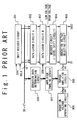
- Fig. 1 shows an example of a data line drive circuit of a display apparatus such as a liquid crystal display of a portable phone, in which a plurality of scanning lines and a plurality of data lines are arranged like a lattice.
- a shift register circuit 901 generates a sampling signal in synchronism with a signal DCLK when a horizontal start signal STH is supplied.
- Image data D0-17 are latched in a data latch circuit A 902 in synchronism with the sampling signal in order and the latched image data are latched in a data latch circuit B 903 at a time in response to the horizontal signal STB.
- the image data latched in the data latch circuit B903 are decoded by a decoder circuit 904.
- a gradation voltage selection circuit 905 is connected to the decoder circuit 904 and selects gradation switches in accordance with the decoded image data.
- a gradation voltage generating circuit 908 has a plurality of resistors connected in series and generates a plurality of voltages suitable for use as the gradation voltages in the display apparatus.
- a buffer amplifier 909 converts the voltages generated by the gradation voltage generating circuit 908 by using a voltage follower circuit, and drives the data lines of the display apparatus through the gradation voltage selection circuit 905.
- the drive circuit needs to incorporate therein a level shift circuit.
- the level shift circuit is arranged upstream relative to the decoder circuit, and [data latch circuit B], [level shift circuit (6)], and [decoder circuit] are arranged in this order, causing the drive circuit to have only 6 level shift circuits.
- a display apparatus incorporated in such a way in a mobile phone is preferably designed to include as small number of level shift circuits as possible in terms of reduction in power consumption. Accordingly, when the image data is of 4 bits or more, the level shift circuit is generally disposed upstream relative to the decoder circuit.
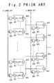
- the decoder circuit is composed of (64+8) number of 3-input NAND circuits 920.
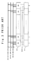
- FIG. 3 shows the detail when the technique for reducing the power consumption is applied to a gradation data determination circuit 906 shown in Fig. 1.
- the gradation data determination circuit 906 is composed of a decoder circuit 910 which is composed of three 6-input NAND circuits and one 3-input NAND circuit, and an RS latch circuit 911 which is connected to the decoder circuit.
- the gradation data determination circuit 906 is configured so that image data buses D0-D17 are connected to the decoder circuit 910 and the determination circuit 906 carries out determination in synchronism with a clock signal DCLK. For example, when even only one "00H” is inputted as image data to the circuit 906 during one horizontal period, the data "00H” is set in the RS latch circuit and the buffer amplifier corresponding to "00H” is set to an enable state by the amplifier enable circuit. If no "00H” is inputted thereto during the one horizontal period, the buffer amplifier corresponding to "00H” is set to a disable state, allowing reduction in the magnitude of current consumed in the buffer amplifier.
- This determination is carried out every horizontal period and a reset signal is supplied every horizontal period to initialize the data contained in the RS latch circuit. In this way, determining the value of image data in synchronism with the clock signal DCLK to set the buffer amplifier corresponding to a gradation, which is not used during the corresponding horizontal period, to the disable state helps to reduce the consumption current.
- the image data is always latched in a line memory (the data latch circuit A and the data latch circuit B) in synchronism with a signal from the CPU. Also, the determination of the image data is carried out in synchronism with the signal from the CPU.
- a portable phone displays a still image in most of the cases and therefore is configured so that a data drive circuit section includes a frame memory and CPU sends image data only when frame image is changed, in order to reduce power consumption. For this reason, a control signal for control of drive circuit and a signal from the CPU are made asynchronous. In other words, a clock signal and image data are supplied only when an image to be displayed is changed.
- the image data in order to display an image, the image data must be driven in a constant period asynchronous with a signal from the CPU.
- the image data are transferred from the frame memory to the line memory all at once in response to a latch signal having the constant period. Therefore, it is necessary to determine the image data stored in the line memory all at once.
- the conventional technique cannot provide a method for determining image data stored in the line memory all at once.
- JP-P2001-272655A a drive circuit of a liquid crystal display is disclosed in Japanese Laid Open Patent Application (JP-P2001-272655A).
- JP-P2001-272655A Japanese Laid Open Patent Application
- one is selected from gradation voltages for 2 n gradations to a positive polarity and a negative polarity to a common voltage as a drive voltage of data lines of a liquid crystal panel based on n-bit digital data signal by using an A/D converter.
- a drive capability is increased by an operational amplifier of a voltage follower connection which can output a rising waveform and a falling waveform, and the gradation voltage is outputted from an output terminal. When the polarity of this output changes every a predetermined period, the output terminal is connected to the common voltage.
- the input of the operational amplifier is set as the gradation voltage for the next polarity in which the current flowing through the operational amplifier becomes the smallest during a period from when the output terminal is connected to the common voltage to when the next gradation voltage for the next polarity is selected by the D/A converter.
- JP-P2001-343944A a drive apparatus of a liquid crystal display is disclosed in Japanese Laid Open Patent Application (JP-P2001-343944A).
- JP-P2001-343944A k-bit data signal corresponding to data lines of a liquid crystal panel is converted to a desired one of 2 k gradation voltages by a D/A converter which is alternately switched between a positive polarity and a negative polarity for every scan of the data lines.
- the drive capability of the gradation voltage is increased by a voltage follower output circuit, and the gradation voltage is outputted to the data lines.
- a logical process is applied to the data signal for n-th scanning and the data signal for (n+1)-th scanning, and the through rate of the voltage follower output circuit in the (n+1)-th scanning is changed in accordance with the logical process result.
- JP-P2002-215108A a drive circuit of a liquid crystal display is disclosed in Japanese Laid Open Patent Application (JP-P2002-215108A).
- a digital video image data is outputted as it is or is outputted after inversion based on a polarity signal which is inverted for every horizontal synchronization period or vertical synchronization period.
- a group of gradation voltages for the positive polarity and a group of gradation voltages for the negative polarity are predetermined to fit with the transmittivity characteristic to the positive application voltage and the transmittivity characteristic to the negative application voltage in the liquid crystal display, and one is selected from the above groups based on the polarity signal.
- One is selected from among the gradation voltages of the selected group based on the digital video image data or the inverted digital video image data, and the selected gradation voltage is applied to a corresponding data electrode.
- a drive circuit is disclosed in Japanese Laid Open Patent Application (JP-P2002-366106A).
- a scanning line inversion drive is carried out to set a voltage level in a scanning period of a counter electrode opposing to a pixel electrode through electro-optical substance to a voltage level different from that in a previous scanning period.
- the voltage level of the counter electrode is set to one of first and second voltage levels.
- the voltage level of the counter electrode is set to the other of the first and second voltage levels.
- the voltage level of the counter electrode is set to the one voltage level of the first and second voltage levels.
- an object of the present invention is to provide a drive circuit of a display apparatus, in which it possible to reduce power consumption of the drive circuit.
- Another object of the present invention is to provide a drive circuit of a display apparatus, in which power consumption of the drive circuit can be reduced by using gradations of image data in a previous line.
- Another object of the present invention is to provide a drive circuit of a display apparatus, in which the drive circuit has a frame memory and power consumption of the drive circuit can be reduced when a video image is displayed, in addition to a still image display.
- a drive circuit of a display apparatus in which a plurality of scanning lines and a plurality of data lines are orthogonalized, include a first data latch circuit which latches image data for every line in response to a horizontal signal; a decoder circuit which decodes the latched image data; and a gradation voltage selection circuit which selects voltage lines based on the decoded image data, to connect each of the plurality of data lines with any of the voltages lines.
- the drive circuit further includes a data determination circuit which generates determination signals based on the selected voltage lines such that each of a plurality of gradation amplifiers is selectively set to an inactive state based on the determination signal; a gradation amplifier circuit which may include the plurality of gradation amplifiers, each of which amplifies a corresponding one of gradation voltages when being in an active state and does not amplify the corresponding gradation voltage when being in an inactive state, the amplified gradation voltage being outputted on a corresponding one of the voltage lines; and an output circuit which drives the plurality of data lines based on the amplified gradation voltages on the voltage lines.
- the drive circuit may further include a bias control circuit which sets each of the plurality of gradation amplifiers to the active state or the inactive state based on the determination signals from the data determination circuit.
- the drive circuit may further include a frame memory which stores the image data for one frame; and a second latch circuit which latches the image data for one line in response to a latch signal, to output to the first latch circuit.
- the drive circuit may further include a data switching circuit which outputs input image data to the frame memory when the input image data is video image data, and outputs the input image data to the second latch circuit when the input image data is still image data.
- the drive circuit may further include a gradation voltage generating circuit which generates a plurality of voltages; and a polarity switching circuit which is provided between the gradation voltage generating circuit and the gradation amplifier circuit to select the gradation voltages from the plurality of voltages generated by the gradation voltage generating circuit in response to a polarity signal.
- the data determination circuit may operate in response to the horizontal signal or in response to the horizontal signal and the polarity signal.
- the gradation voltage selection circuit may include a plurality of gradation selection switches which select one of the voltage lines for each of the plurality of data lines based on the decoded image data; and a first switch which is provided for each of the plurality of gradation selection switches to connect an input terminal of each of the plurality of gradation selection switches with a higher voltage or a lower voltage power supply.
- the output circuit may include a second switch which is provided for each of the plurality of gradation selection switches to connect an output terminal of each of the plurality of gradation selection switches with the lower voltage or the higher voltage; and a third switch which is provided for each of the plurality of gradation selection switches to switch between the output terminal of each of the plurality of gradation selection switches and the output circuit.
- the data determination circuit generates the determination signals based on a voltage on each of the voltage lines.
- the drive circuit may further include a command control circuit which always sets the third switches which are not connected to the plurality of data lines of the display apparatus to an off state when the number of pixels of the frame memory is more than the number of pixels of the display apparatus.
- the gradation voltage selection circuit may include a plurality of gradation selection switches which select one the voltage lines for each of the plurality of data lines based on the decoded image data; a first switch which is provided for each of the plurality of gradation selection switches to connect an input terminal of each of the plurality of gradation selection switches with a higher voltage; and a second switch which is provided for each of the plurality of gradation selection switches to connect the input terminal of each of the plurality of gradation selection switches with a lower voltage.
- the output circuit may include a third switch which is provided for each of the plurality of gradation selection switches to connect an output terminal of each of the plurality of gradation selection switches with the lower voltage; a fourth switch which is provided for each of the plurality of gradation selection switches to connect the output terminal of each of the plurality of gradation selection switches with the higher voltage; and a fifth switch (206) which is provided for each of the plurality of gradation selection switches to switch between the output terminal of each of the plurality of gradation selection switches and the output circuit.
- the data determination circuit generates the determination signals based on an output voltage of each of the plurality of gradation selection switches.
- the drive circuit may further include a command control circuit which always sets the third and fifth switches which are not connected to the plurality of data lines of the display apparatus to an off state when the number of pixels of the frame memory is more than the number of pixels of the display apparatus.
- the drive circuit may further include the gradation voltage selection circuit sets the plurality of gradation amplifiers to the inactive state during a period during which there are not the plurality of scanning lines corresponding to the image data, when the number of pixels of the frame memory is more than the number of pixels of the display apparatus.
- the data determination circuit may include a counter which is provided to count the gradation voltages selected by the gradation voltage selection circuit.
- the data determination circuit may change a period during which each of the plurality of gradation amplifiers is in the active state based on a count value of the counter such that the period is shorter as the count value is less.
- each of the plurality of gradation amplifiers may include a constant current source, and an output stage.
- the data determination circuit sets a current value of the constant current source to 0 when the gradation amplifier is in the inactive state, and the output stage to a high impedance state.
- the gradation amplifier circuit may include a first group of gradation amplifiers, each of which has N-channel transistors as differential input transistors; and a second group of gradation amplifiers, each of which has P-channel transistors as the differential input transistors.
- Fig. 4 is a block diagram showing the configuration of a display apparatus, e.g., a liquid crystal display device to which the present invention is applied.
- a display apparatus 1000 used for a portable phone, etc. is connected to a CPU 2, and displays an image in response to a signal 12 from the CPU 2.
- the display apparatus 1000 includes a display unit having a plurality of scanning lines and a plurality of data lines arranged in a matrix of rows and columns.
- the display apparatus 1000 contains a data line drive circuit 1, an interface circuit 3, a RAM control circuit 4, a command control circuit 5, a timing control circuit 6, a scanning line drive circuit 7, an oscillation circuit 8 a timing generating circuit 9, a power supply circuit 10, and a Vcom circuit 11.
- the data line drive circuit 1 drives the data lines of the display unit and contains a later-described frame memory 101 and a data determination circuit 107.
- the interface circuit 3 is connected to the CPU 2 to interface.
- the RAM control circuit 4 is connected to the interface circuit 3 and the drive circuit 1.
- the RAM control circuit 4 controls a write address of the frame memory 101 and so on.
- the command control circuit 5 is connected to the interface circuit 3, the drive circuit 1 and the timing control circuit 6.
- the command control circuit 5 inputs data necessary to drive the display unit such as setting data in a gamma circuit and a drive frequency, a drive voltage and the number of pixels of the frame memory 101 from the CPU 2 via the interface circuit 3, and holds data written in an EEPROM (not shown) therein.
- the command control circuit 5 controls the drive circuit 1 and the timing control circuit 6.
- the oscillation circuit 8 generates a clock signal RCLK asynchronous with the signal supplied from the CPU 2.
- the timing generating circuit 9 generates signals such as a vertical signal VS, a horizontal signal STB and a polarity signal POL necessary to drive the display unit based on the clock signal supplied from the oscillation circuit 8.
- the timing control circuit 6 generates timing signals to control drive timings of the display unit, and the drive timings are supplies to the data line drive circuit 1, the scanning line drive circuit 7, the power supply circuit 10, and the Vcom circuit 11.
- the power supply circuit 10 generates voltages for the display apparatus 1000 in response to the drive timing from the timing control circuit and supplies to various sections such as the data line drive circuit 1, the scanning line drive circuit 7 and the Vcom circuit 11.
- the voltages used are generated by the power supply circuit 10 to drive the data lines, the scanning lines and the common electrodes of the display unit.
- the Vcom circuit 11 drives common electrodes in accordance with the drive timing from the timing control circuit using the voltages.
- the scanning line drive circuit 7 drives the scanning lines in response to the drive timing.
- circuits are not always necessarily formed on the same substrate or a circuit board.
- the power supply circuit 10, the scanning line drive circuit 7 and the Vcom circuit 11 may be formed on another substrate or board. Also, a part or the whole of the circuits may be manufactured on a glass substrate.
- the signal 12 supplied from the CPU would include a chip select signal, a write signal, a read signal, a data/command selection signal, a reset signal and so on, all the signals are collectively shown as the signal 12.
- the frame memory 101 can store image data for one frame, and still image data supplied from the CPU 2 is written in the frame memory 101.
- the image data for one line stored in the frame memory 101 is transferred to a data latch circuit A 102 all at once in response to a latch signal LAT from the timing control circuit 6.
- a write signal supplied from the CPU 2 and the latch signal LAT overlap in timing, a write instruction from the CPU 2 to write to the frame memory 101 is carried out with a higher priority.
- the image data latched in the data latch circuit A 102 is transferred all at once to and latched by the data latch circuit B 103 in response to the horizontal signal STB and a polarity signal POL, and is held for a current horizontal period.
- the image data latched in the data latch circuit B 103 is decoded by a decoder circuit 104 which is composed of such as NAND circuits for a level shift circuit.
- a gradation voltage generation circuit 109 generates a plurality of voltages.
- a polarity switching circuit 110 is provided so that a certain voltage to be output from the circuit 110 is switched between a group of positive gamma voltages and a group of negative gamma voltages in response to a polarity signal POL, in order to output the certain voltage as gradation voltages.
- a gradation amplifier circuit 111 contains a plurality of gradation amplifiers which amplify the gradation voltages from the polarity switching circuit 110, and the amplified gradation voltages are supplied to a gradation voltage selection circuit 105.
- the gradation voltage selection circuit 105a contains a plurality of gradation selection switches. The gradation selection switches are activated in accordance with the decoded image data from the decoder circuit. The amplified gradation voltages corresponding to the activated gradation selection switches are outputted to an output circuit 106 and are used to drive the data lines.
- a data determination circuit 107 generates determination signals for a current horizontal period from the amplified gradation voltages corresponding to the activated gradation selection switches for the current horizontal period.
- a bias control circuit 108 controls the gradation amplifiers of the gradation amplifier circuit 111 based on the determination signals during the current horizontal period.
- the gradation voltage generation circuit 109 contains a resistor string circuit in which a plurality of resistors are connected in series.
- the gradation voltage generation circuit 109 generates a plurality of voltages using the resistor string circuit to allow the voltages to fit to the gamma characteristic of the display unit.
- the liquid crystal display needs to be alternately driven for prevention of degradation of liquid crystal. For this reason, a positive voltage and a negative voltage are alternately applied to the common electrode of the liquid crystal display and the polarity of a voltage to be applied is changed in a predetermined period.
- the polarity switching circuit 110 is provided to allow a gradation voltage to switch between the positive gamma voltages and the negative gamma voltages.
- the gradation voltage generation circuit 109 and the polarity switching circuit 110 make up voltage generation means.
- the plurality of gradation voltages from the polarity switching circuit 110 are amplified respectively by the plurality of gradation amplifiers 111 of the gradation amplifier circuit 111 and are supplied to the gradation voltage selection circuit 105.
- the CPU 2 when a still image such as a photograph is displayed, the CPU 2 does not necessarily always transfer image data, but may transfer the data only when the image changes. In this way, because whether the image data 12 from the CPU 2 is inputted to the drive circuit or not is random, the signal used in a drive circuit system needs to be asynchronous with the signal 12 from the CPU 2. For this reason, a clock signal of the drive circuit system is generated by the oscillation circuit 8 which is composed of a capacitor and a resistor. Signals such as the horizontal signal STB, the vertical signal VS, the latch signal LAT, the polarity signal POL which are necessary to drive the display unit are generated by the timing generating circuit 9 based on the clock signal from the oscillation circuit 8.
- Fig. 7 shows the configuration of the gradation voltage generation circuit 109, the polarity switching circuit 110 and the gradation amplifier circuit 111.
- the gradation voltage generation circuit 109 includes 500 resistors R1 to R500 with the same resistance and input buffers 301.
- the resistors R1 to R500 are connected in series and the input buffers 301 are connected between some of connection nodes of the resistors. Individual voltages can be obtained from individual connection nodes.
- the polarity switching circuit 110 is composed of a switching unit 303 having 64 switches for supply of positive voltages and a switching unit 304 having 64 switches for supply of negative voltages.
- the polarity switching circuit 110 connects 64 predetermined voltages chosen out of the 500 voltages generated by the gradation voltage generation circuit 109 to the input terminals of each of the switch units 303 and 304 to allow the 64 predetermined voltages to fit the gamma characteristic of liquid crystal.
- the polarity switching circuit 110 operates so that when the polarity signal POL is "H", the switches SWP1 to SWP64 of the switching unit 303 are turned on and the switches SWN1 to SWN64 in the switching unit 304 are turned off.
- the switches SWP1 to SWP64 of the switching unit 303 are turned off, and the switches SWN1 to SWN64 of the switching unit 304 are turned on.
- the 64 selected voltages are supplied to the gradation amplifier circuit 111.
- Each of the gradation amplifiers may be of a voltage follower type (with the gain of one). However, the gradation amplifier 111 does not need to be of a voltage follower type.
- each of the gradation amplifiers is constituted by an operational amplifier 403 with loads 401 and 402 and has a gain larger than one, as shown in Figs. 8A and 8B.
- the gradation amplifiers are grouped into a group of gradation amplifiers 306 and a group of gradation amplifiers 307.
- the gradation amplifier 306 has a circuit configuration shown in Fig.
- Fig. 9A shows an input - output characteristic shown in Fig. 9B.
- Fig. 9C shows an equivalent circuit of the gradation amplifier 306.
- N-channel transistors Q1 and Q2 are used for input transistors of a differential stage in the gradation amplifier 306.
- the gradation amplifier 307 has a circuit configuration shown in Fig. 10A and an input - output characteristic shown in Fig. 10B.
- Fig. 10C shows an equivalent circuit of the gradation amplifier 307.
- P-channel transistors Q11 and Q12 are used for input transistors of a differential stage in the gradation amplifier 307.
- the dynamic range can be secured on the higher voltage side indicated by the input-output characteristic shown in Fig. 9B. Also, if the input transistors of the differential stage are of a P-channel type, the dynamic range can be secured on the low voltage side indicated by the input- output characteristic shown by in Fig. 10B. Therefore, the gradation amplifier circuit 111 consuming low power can be formed, using two types of amplifiers.
- the gradation amplifier circuit 111 includes 2 m gradation amplifiers when the image data is m bits, and these 2 m gradation amplifiers are constituted by k (k is an integer more than 0) number of N-channel gradation amplifiers 306 and the 2 m -k number of P-channel gradation amplifiers 307.
- the bias control circuit 108 shown in Fig. 5 is provided to control current supplied by a constant current source of each of the gradation amplifiers 306 and 307.
- the bias control circuit 108 is composed of a constant current source 501, an N-channel transistor Q31 and 64 sets of N-channel transistors Q32 and Q33 on the N-channel side and a constant current source 502, a P-channel transistor Q34 and 64 sets of P-channel transistors Q35 and Q36 on the P-channel side, and 64 inverters 503.
- Each of the 64 determination signals from the data determination circuit is connected to the gates of the N-channel transistors Q33 and the gates of the P-channel transistors Q36.
- Each of the 64 determination signals inverted by the inverters 503 is connected to the gates of the N-channel transistors Q32 and the gates of the P-channel transistors Q35.
- the bias control circuit 108 individually controls a current value of each of the 64 constant current sources in each of the gradation amplifiers 306 and 307 based on the determination signals from the data determination circuit 107.
- the bias terminal BNn is connected to the gate of the constant current source transistor Q5 of each gradation amplifier 306, and the bias terminal BPn is connected to the gate of the constant current source transistor Q15 of each gradation amplifier 307.
- the voltage of the terminal BNn is GND and the voltage of the terminal BPn is VDD in the bias control circuit 108, allowing the individual amplifiers to be inactive.
- the voltage of the terminal BNn is set to a predetermined voltage N and the voltage of the terminal BPn is set to a predetermined voltage P.
- current of a predetermined magnitude flows through the constant current source of each of the gradation amplifiers 306 and 307, allowing the amplifiers to be active.
- the output stage of each of the gradation amplifiers 306 and 307 contains a P-channel transistors (Q6 or Q16) and a N-channel transistors (Q7 or Q17), as shown in Fig. 9A and 10A.
- the determination signal Cn supplied from the data determination circuit 107 to the bias control circuit 108 is set to "H"
- a signal CnB is set to "L” (CnB means an inverted signal of the determination signal Cn).
- the transistor Q8 turns on so that the gate voltage of the transistor Q6 becomes VDD, resulting in the transistor Q6 turning off.
- the transistor Q9 turns on so that the gate voltage of the transistor Q7 becomes GND, resulting in the transistor Q7 turning off. Therefore, the output of the output stage becomes a high impedance state. Also, the gate voltage BNn of the constant current source Q5 becomes GND and the current value of constant current source Q5 becomes 0. Therefore, the N-channel gradation amplifier 306 becomes an inactive state. In the same way, the transistor Q18 turns on so that the gate voltage of the transistor Q16 becomes VDD, resulting in the transistor Q16 turning off. Also, the transistor Q19 turns on, so that the gate voltage of the transistor Q17 becomes GND, resulting in the transistor Q17 turning off. Therefore, the output of the output stage becomes a high impedance state.
- the gate voltage BPn of the constant current source Q15 becomes VDD, so that the current value of constant current source Q15 becomes 0, and the P-channel gradation amplifier becomes an inactive state. In this way, the gradation amplifier can be set to the inactive state based on the determination signal.
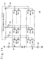
- Fig. 12 shows the gradation amplifier circuit 111, the gradation voltage selection circuit 105 and the output circuit 106.
- the gradation amplifier circuit 111 is composed of a plurality of gradation amplifiers. Each of a plurality of switches 202 is a part of the gradation amplifier, as shown in the equivalent circuits of Figs. 9C and 10C.
- the gradation voltage selection circuit 105 is composed of 64 gradation lines 204, switches 203a and gradation selection switches 205.
- the gradation lines 204 are connected to output terminals 202 of the gradation amplifiers 306 and 307 (refer to Figs. 9A and 10A) in the gradation amplifier circuit 111.
- the switches 203a are connected to the respective gradation lines 204.
- Each of the gradation selection switches 205 is composed of 64 analog switches and is connected to the gradation lines 204. Also, the gradation lines 204 are connected to the data determination circuit 107.
- the output circuit 106 is composed of switches 206 and switches 207a. It would be apparent to those skilled in the art that the present driving circuit may be configured to include the switches 207a in the gradation voltage selection circuit 105 instead of the output circuit 106.
- the switches 206 are provided between the data lines of the display unit and the output of the gradation selection switches 205.
- the switches 207a are provided between the outputs of the gradation selection switches 205 and supplies the voltage of GND or VDD.
- all the switches 203a are connected to VDD and all the switches 207a are connected to GND, or all the switches 203a are connected to GND and all the switches 207a are connected to VDD. If the switches 203a and the switches 207a are connected to the same voltage supply, a potential change at each of the gradation lines 204 cannot be detected.
- the data determination circuit 107 carries out the data determination in cooperation with the decoder circuit 104, the gradation voltage selection circuit 105 and the output circuit 106.
- the image data read out from the frame memory 101 is transferred to and latched by the data latch circuit A 102 in response to the latch signal LAT.
- the above-mentioned determination signals Cn are all set to "H" regardless of the image data at the time t2 in Figs. 14A to 14G in response to a timing signal from the time control circuit 6.
- all the switches 202 are turned off and all the gradation amplifiers 201 are set to an inactive state.
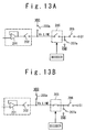
- Fig. 13A shows the states of the switches in this case.
- the reason why the switch 206 is set to an off state is to prevent the data line of the display unit from being driven by the voltage of the corresponding gradation line during the data determination process.
- the image data is transferred from the data latch circuit A 102 to the data latch circuit B 103 in response to the horizontal signal STB, and is latched therein.
- the decoder circuit 104 decodes the image data latched in the data latch circuit B 103.
- the switches 203a are turned on to precharge or pull up all of the gradation lines 204 to the voltage supply VDD in response to a timing signal from the time control circuit 6.
- Fig. 13B shows the states of the switches.
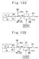
- all of the switches 203a are turned off and then all of the switches 207a are turned on in response to a timing signal from the time control circuit 6.
- Figs. 13C and 13D show how the switches operate.
- the data determination circuit 107 contains latch circuits (not shown), and latches the voltage level of each of the 64 gradation lines 204 as "1" when the gradation line 204 holds the level of VDD and "0" when the gradation line 204 holds the level of GND at the time t4 in Figs. 14A to 14G.
- a capacitor though not shown, is connected to each gradation line.
- the data determination circuit 107 generates the determination signals based on the latched voltage levels and drives the bias control circuit 108.
- the bias control circuit 108 generates the signals BN1 to BN64 and BP1 to BP64.
- the gradation amplifiers 201 stay in an inactive state or are changed to an active state depending on the signals BN1 to BN64 and BP1 to BP64 from the bias control circuit 108.
- the switches 202 are selectively turned on based on the determination signals from the data determination circuit 107.
- the switches 206 are turned on in response to a timing signal from the time control circuit 6. In this way, the gradation voltages are applied to the data lines by only the gradation amplifiers in an active state.
- the image data for one horizontal line is determined and unnecessary gradation amplifiers are turned to an inactive state based on the determined image data, allowing the gradation amplifier circuit to operate at low power and further permitting the display unit to be driven with low power.
- the gradation amplifiers consumes about 10 ⁇ A
- the data determination circuit 107 may be constituted of latch circuits (not shown), resulting in reduction of the circuit scale.
- the drive circuit of the display unit is manufactured to contain the frame memory 101 as in a semiconductor integrated circuit
- the number of pixels of the display unit and the number of pixels of the frame memory are different.
- the switches 206 which are not connected to the data lines are always turned off based on an instruction from the command control circuit 5. Also, because 16 scanning lines are not connected, the gradation amplifiers of the data line drive circuit 1 are set to inactive state during a period corresponding to the un-connected scanning lines in response to the timing signals supplied from the time control circuit 6 based on an instruction from the command control circuit 5. Thus, power consumption can be reduced.
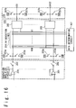
- Fig. 15 is a block diagram of the data line drive circuit 1 according to the second embodiment of the present invention
- Fig. 16 shows the circuit configuration which contains the data determination circuit 107 for the data determination.
- the second embodiment is different from the first embodiment in a part of the circuit structure.
- the switches 206 which are connected to the data lines are set to the off state, and any voltage is not applied to the data lines in the case of the data determination.
- the voltage of GND or VDD is applied in the case of the data determination.
- the switches 203a which are connected to the gradation lines 204 and the switches 207a which are connected to the outputs of the gradation selection switches 205 are common between the first and second embodiments.
- switches 203b which are connected to the gradation lines 204 and switches 207b which are connected to the gradation selection switches 205 are added in the second embodiment.
- the switches 203a are connected to VDD and the switches 207a are connected to the GND, and the switches 203b are connected to the GND and the switches 207b are connected to VDD.
- Figs. 17A to 17J show time charts of the operation. Also, the operating states corresponding to those of Figs. 13A to 13D are shown in Figs. 18A to 18D.
- the difference of the second embodiment from the first embodiment in the operation is in that when the image data is determined, the output circuit is not in the high impedance state and outputs voltages in accordance with the polarity signal POL.
- the image data stored in the frame memory 101 is read out and transferred to the data latch circuit A 102, and latched therein in response to the latch signal LAT.
- the above-mentioned determination signals Cn are all set to "H" together regardless of the image data in response to a timing signal from the time control circuit 6.
- the switches 202 are turned off and all the gradation amplifiers 201 are set to the inactive state.
- the gradation selection switches 205 are turned off regardless of the gradation data in response to a timing signal from the time control circuit 6.
- the switches 203a are turned on in response to a timing signal from the time control circuit 6 and the gradation lines are precharges to the voltage VDD (Fig. 18A).
- the polarity signal POL is inverted and the switches 203b are turned on and the gradation lines are precharged to the voltage GND (Fig. 18C).
- the image data is transferred from the data latch circuit A 102 to the data latch circuit B 103 in response to the horizontal signal STB, and latched therein.
- the decoder circuit 104 decodes the image data latched in the data latch circuit 103.
- the switches 203a are turned off in response to a timing signal from the time control circuit 6, and the gradation selection switches 205 are selectively turned on and in accordance with the image data decoded by the decoder circuit 104 in response to a timing signal from the time control circuit 6.
- the switches 207a are turned on in response to a timing signal from the time control circuit 6.
- the data lines are fixed on GND.
- the gradation lines are set to the voltage GND when the gradation selection switches 205 are turned on.
- the gradation lines corresponding to the gradation selection switches 205 in the off state keeps the voltage VDD.
- the voltage levels of the gradation lines corresponding to the switches 205 are latched in the latch circuit (not shown) of the data determination circuit 107 (Fig. 18B).
- the polarity signal POL is inverted, the switches 203b are turned off, and the switches 207b are turned on.
- the data lines are fixed on of the voltage VDD.
- the gradation lines 204 corresponding to the gradation selection switch 205 set to the on state in accordance with the image data are set to the voltage VDD (Fig. 18D).
- the gradation line 204 corresponding to the gradation selection switches 205 in the off state keeps the voltage GND.
- the voltage levels of the 64 gradation lines 204 should be latched by the latch circuit of the data determination circuit 107 as "1" in case of the voltage VDD and as "0" in case of the voltage GND.
- a circuit (not shown) for inverting the image data which is determined in accordance with the polarity signal POL is necessary to the data determination circuit 107 in addition to the latch circuit.
- the switches 207a are turned off in response to the timing signal from the time control circuit 6 at the time t6a in Figs. 17A to 17J.
- the data determination circuit 107 generates the determination signals based on the latched voltage levels and drives the bias control circuit 108.
- the bias control circuit 108 generates the signals BN1 to BN64 and BP1 to BP64.
- the gradation amplifiers 201 are kept to the inactive state or set to the active state based on the signals BN1 to BN64 and BP1 to BP64 from the bias control circuit 108.
- the switches 202 are selectively turned on based on the determination signals from the data determination circuit 107.
- the switches 206 are turned on in response to a timing signal from the time control circuit 6. In this way, the gradation voltages are applied from only the gradation amplifiers in the active state to the data lines.
- the switches 207b are turned off, and the gradation amplifiers 201 are kept to the inactive state or is set to the active state based on the determination result by the data determination circuit 107 in response to the signals from the bias control circuit 108.
- the gradation voltages determined in accordance with the image data can be applied to the data lines.
- the switches connected to the data lines are set to the high impedance during the data determination.
- the data lines are fixed on VDD or GND. This is to prevent that the data lines are inverted with the influence of the cross talk when Vcom is inverted so that a voltage higher than the voltage endurance is not applied to the drive circuit system.
- the switch 206 in the first embodiment may be added to the second embodiment.
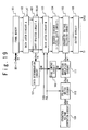
- Fig. 19 shows a block diagram of the data line drive circuit 1 according to the third embodiment of the present invention.
- the position of a shift register circuit A 601 is different, compared with the conventional structure shown in Fig. 1
- the shift register circuit 901 is provided in the front-stage of the data latch circuit A 902 and has the function to generate the sampling signal such that the image data is latched in the data latch circuit A 902 in order.
- the shift register circuit 601 is provided in the back-stage of the data latch circuit A 102, and has the function to transfer the image data latched in the data latch circuit A 102 to the data determination circuit 107 in order in synchronous with a clock signal RCLK.
- Fig. 20 shows a data determining section.
- the shift register circuit A 601 is composed of two flip-flops 602 and switches 603 and 604 for every bit data.
- the data determination circuit 107 is composed of three 6-input NANDs, one 3-input NAND and the latch circuit, although being not shown in the figure.
- the image data stored in the frame memory 101 is transferred to the data latch circuit A 102 with a line memory function in synchronous with the latch signal LAT which is asynchronous with the signal 12 of the CPU 2.
- the image data latched in the data latch circuit A 102 is transferred to the data determination circuit 107 in order in synchronism with the clock signal RCLK which is asynchronous with the signal 12 of the CPU 2, by the shift register circuit A 601 provided in the back-stage of the data latch circuit A 102.
- the clock signal RCLK is stopped when the image data for one line is determined and the data determination is ended.
- the image data is transferred to the data latch circuit B 103 in response to the horizontal signal STB, the gradation selection switches 205 are selected in accordance with the image data and the data lines of the display unit are driven.
- the image data determined by the data determination circuit 107 is reset and the data determination for the next line is started.
- a counter (not shown) is added to the data determination circuit 107, it is possible to determine by how many data line the each gradation is used.
- Low power consumption drive can be achieved by providing the function to change the drive time in accordance with this counter value, as shown in Figs. 21A and 21B.
- the gradation amplifier in the active state is only one, and the load of the gradation amplifier becomes very large, resulting in a large output delay.
- the number of gradation amplifiers in the active state is two or more. In this case, the power consumption becomes large but the output delay becomes small, because the loads are distributed and the capacitive load of the gradation amplifier becomes small.
- the gradation amplifiers As a result, it is possible to drive the gradation amplifiers in a short active time. Specifically, when the right half of the display screen is white and the left half of the display screen is black, two gradation amplifiers are in the active state. However, the output delay time becomes short because the capacitive loads of the gradation amplifiers become a half, compared with a case that the whole of screen is the same color. In the same way, when a 64-color display is carried out at the same time, the power consumption of the gradation amplifiers becomes 64 times, compared with a case that the whole screen is displayed in a black or white color. However, it is possible to reduce the power consumption largely by changing the active timings of the gradation amplifiers in accordance with the number kinds of the image data.
- the data determination circuit 107 has only the function to activate the gradation amplifiers 201 in case of data of "1" and to inactivate it in case of the data of "0", because the data held by the latch circuit (not shown) is binary data of 0 or 1.
- it is possible to change an active time period by allocating a constant current source function to the switches 207a of Fig. 12 and an A/D conversion function to the data determination circuit 107, moreover by using the determination data of plural bits to add a time data to the determination signal.
- Fig. 22 shows the detail of the data determination circuit 107 which has the A/D conversion function.
- A/D conversion circuit 803 It is enough to provide one A/D conversion circuit 803, and a sample hold circuit 801 is provided for each gradation line to have a switch and a capacitor.
- the A/D conversion circuit 803 is switched between the gradation lines in order by a switch circuit 802 to measure a voltage of the connected gradation line.
- the measured voltage is latched in the latch circuit 804.
- the bias time control circuit 805 changes the active time periods of the gradation amplifiers 201 in accordance with the number of data latched in the latch circuit 804, like the third embodiment. Thus, the power consumption can be reduced.
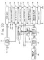
- Fig. 23 shows a block diagram of the data line drive circuit 1 according to the fifth embodiment of the present invention.
- the fifth embodiment is different from the first embodiment in that a mode in which the image data is stored in the frame memory and a mode in which the image data is not stored can be selected.
- a mode in which the image data is stored in the frame memory In the portable phone, a still image is displayed in many cases but a video image is sometimes displayed. When the vide image is displayed, the power consumption becomes large when the video image data is written in the frame memory 101. For this reason, it is better to transfer the video image data directly to the data latch circuit A 102 as a line memory without writing the video image data in the frame memory 101 in case of the video image display.
- the shift register circuit 702 is provided for this purpose. Also, a data switching circuit 701 and an RGB switching circuit 703 are provided to switch whether the image data is transferred to the frame memory 101 or the data latch circuit A 102 in accordance with the still image display or the video image display.
- the input is switched by an interface circuit 3.
- the video image data is transferred to the data latch circuit A 102 directly by the data switching circuit 701 and the RGB switching circuit 703.
- image data is transferred to the frame memory 101 by the data switching circuit 701.
- the data shift register circuit 702 stops the operation in the still image display.
- the operation of the circuit after the data latch circuit A 102 is the same as the operation in the first embodiment.
- the data switching circuit 701 and the RGB switching circuit 702 may be added to the structure of the third embodiment shown in Fig. 19.
- FIG. 24B there is a case that signal lines when the image data is supplied from the CPU 2 are different depending on the still image data or the video image data.
- MODE 1 and 4 are mainly used in the case of the vide image display
- MODE 2 and 3 are mainly used in the case of the still image.
- the switching is carried out by the interface circuit 3.
- the power consumption can be reduced because the gradation amplifiers are made active or inactive in accordance with the image data.
- image data from the frame memory are collectively determined like the first embodiment, it is possible to reduce the number of circuit components of the data determination circuit.
- the NAND circuits are used for the data determination circuit as in the conventional example, 64 6-input NAND are necessary for every data line and 768 transistors are necessary.
- the decoder circuit which has been originally provided is used, and the new components are the plurality of switches connected to the gradation lines and the switches of the output circuit which are connected to the data lines. Therefore, the number of necessary components can be reduced largely.
- the low power consumption drive can be achieved by adding a counter function to the data determination circuit and by controlling the active time period of the gradation amplifier in accordance with the number of data of the image data.
Landscapes
- Engineering & Computer Science (AREA)
- Health & Medical Sciences (AREA)
- Chemical & Material Sciences (AREA)
- Theoretical Computer Science (AREA)
- General Physics & Mathematics (AREA)
- Computer Hardware Design (AREA)
- Physics & Mathematics (AREA)
- Crystallography & Structural Chemistry (AREA)
- Rehabilitation Therapy (AREA)
- Pain & Pain Management (AREA)
- Public Health (AREA)
- Veterinary Medicine (AREA)
- General Health & Medical Sciences (AREA)
- Animal Behavior & Ethology (AREA)
- Life Sciences & Earth Sciences (AREA)
- Physical Education & Sports Medicine (AREA)
- Epidemiology (AREA)
- Mechanical Engineering (AREA)
- Control Of Indicators Other Than Cathode Ray Tubes (AREA)
- Liquid Crystal Display Device Control (AREA)
- Transforming Electric Information Into Light Information (AREA)
Abstract
In a drive circuit of a display apparatus
with scanning lines and data lines are orthogonalized,
a first data latch circuit (103) latches image data
for every line in response to a horizontal signal. A
decoder circuit (104) decodes the latched image data.
A gradation voltage selecting circuit (105) selects
voltage lines based on the decoded image data, to
connect each of the plurality of data lines with any
of the voltages lines. A data determining circuit
(107) generates determination signals based on the
selected voltage lines such that each of a plurality
of gradation amplifiers is selectively set to an
inactive state based on the determination signal. A
gradation amplifier circuit (111) includes the
plurality of gradation amplifiers, each of which
amplifies a corresponding one of gradation voltages
when being in an active state and does not amplify the
corresponding gradation voltage when being in an
inactive state, and the amplified gradation voltage
being outputted on a corresponding one of the voltage
lines. An output circuit (106) drives the plurality
of data lines based on the amplified gradation
voltages on the voltage lines.
Description
The present invention relates to a drive
circuit of a display apparatus which has a frame
memory.
Fig. 1 shows an example of a data line drive
circuit of a display apparatus such as a liquid
crystal display of a portable phone, in which a
plurality of scanning lines and a plurality of data
lines are arranged like a lattice. A shift register
circuit 901 generates a sampling signal in synchronism
with a signal DCLK when a horizontal start signal STH
is supplied. Image data D0-17 are latched in a data
latch circuit A 902 in synchronism with the sampling
signal in order and the latched image data are latched
in a data latch circuit B 903 at a time in response to
the horizontal signal STB. The image data latched in
the data latch circuit B903 are decoded by a decoder
circuit 904. A gradation voltage selection circuit
905 is connected to the decoder circuit 904 and
selects gradation switches in accordance with the
decoded image data. A gradation voltage generating
circuit 908 has a plurality of resistors connected in
series and generates a plurality of voltages suitable
for use as the gradation voltages in the display
apparatus. A buffer amplifier 909 converts the
voltages generated by the gradation voltage generating
circuit 908 by using a voltage follower circuit, and
drives the data lines of the display apparatus through
the gradation voltage selection circuit 905.
Because the voltage used to drive the display
apparatus such as the liquid crystal display is
generally higher than the voltage to be used in a
logic circuit section such as the shift register
circuit and the data latch circuit, the drive circuit
needs to incorporate therein a level shift circuit.
In this case, the level shift circuit is provided
before or after the decoder circuit from the viewpoint
of reduction in the number of bits of the image data
and power consumption. For example, when the image
data is of 6 bits (26 = 64 gradations) and the level
shift circuit is disposed downstream (when viewing
circuit components in a data stream direction)
relative to the decoder circuit, [data latch circuit
B], [decoder circuit (64 x 6-input NAND)], and [64
level shift circuits] are arranged in this order,
causing the drive circuit to have 64 level shift
circuits. On the other hand, if the level shift
circuit is arranged upstream relative to the decoder
circuit, and [data latch circuit B], [level shift
circuit (6)], and [decoder circuit] are arranged in
this order, causing the drive circuit to have only 6
level shift circuits. Because large transient current
flows through the level shift circuit, a display
apparatus incorporated in such a way in a mobile phone
is preferably designed to include as small number of
level shift circuits as possible in terms of reduction
in power consumption. Accordingly, when the image
data is of 4 bits or more, the level shift circuit is
generally disposed upstream relative to the decoder
circuit.
However, when the level shift circuit is
disposed upstream relative to the decoder circuit in
this way, circuits to be disposed downstream relative
to the level shift circuit need to be fabricated with
high-voltage endurance. Therefore, a new problem
arises in that the scale of drive circuit becomes
large. In order to solve this problem, as shown in
Fig. 2, it could be considered that bits of the image
data are divided into three upper bits and three lower
bits to make the circuit scale of the decoder circuit
small. That is, 64 gradation switches 922 are
controlled based on the three upper bits and are
connected to the gradation voltages of V1 to V64
respectively. Eight gradations are selected from
among the 64 gradations based on the three lower bits
and one gradation is further selected from among the
eight gradations based on the 3 upper bits. The
decoder circuit is composed of (64+8) number of 3-input
NAND circuits 920.
An example of a method of reducing the power
consumption of the drive circuit would be a technique
disclosed in Japanese Laid Open Patent Application
(JP-P2002-108301A). In this conventional example,
image data D0 - D17 are determined and the power
consumption of buffer amplifiers (voltage follower
circuits) which are not used is reduced by an
amplifier enable circuit. The image data are supplied
in synchronism with a clock signal DCLK. Fig. 3 shows
the detail when the technique for reducing the power
consumption is applied to a gradation data
determination circuit 906 shown in Fig. 1. The
gradation data determination circuit 906 is composed
of a decoder circuit 910 which is composed of three 6-input
NAND circuits and one 3-input NAND circuit, and
an RS latch circuit 911 which is connected to the
decoder circuit. The reason why the three 6-input
NAND circuits are used is that the image data is
transferred in units of pixels and the image data has
a 6-bit width to represent red, green, and blue for
color display. When data is transferred in units of
two pixels, the seven (=6+1) sets of 6-input NAND
circuits are necessary. Because liquid crystal
display device is not a device capable of emitting
light and in addition, a drive voltage is the same
irrespective of color to be displayed, 64 decoder
circuits 910 and 64 RS latch circuits 911 are
necessary. Signs of "00H" and "3FH" included in the
decoder circuit and shown in Fig. 24 means that image
data is represented by "000000 = 00H" and "111111 =
3FH" (hereinafter, in case of hexadecimal notation, H
is added).
The gradation data determination circuit 906
is configured so that image data buses D0-D17 are
connected to the decoder circuit 910 and the
determination circuit 906 carries out determination in
synchronism with a clock signal DCLK. For example,
when even only one "00H" is inputted as image data to
the circuit 906 during one horizontal period, the data
"00H" is set in the RS latch circuit and the buffer
amplifier corresponding to "00H" is set to an enable
state by the amplifier enable circuit. If no "00H" is
inputted thereto during the one horizontal period, the
buffer amplifier corresponding to "00H" is set to a
disable state, allowing reduction in the magnitude of
current consumed in the buffer amplifier. This
determination is carried out every horizontal period
and a reset signal is supplied every horizontal period
to initialize the data contained in the RS latch
circuit. In this way, determining the value of image
data in synchronism with the clock signal DCLK to set
the buffer amplifier corresponding to a gradation,
which is not used during the corresponding horizontal
period, to the disable state helps to reduce the
consumption current.
In such a technique, the image data is always
latched in a line memory (the data latch circuit A and
the data latch circuit B) in synchronism with a signal
from the CPU. Also, the determination of the image
data is carried out in synchronism with the signal
from the CPU. However, a portable phone displays a
still image in most of the cases and therefore is
configured so that a data drive circuit section
includes a frame memory and CPU sends image data only
when frame image is changed, in order to reduce power
consumption. For this reason, a control signal for
control of drive circuit and a signal from the CPU are
made asynchronous. In other words, a clock signal and
image data are supplied only when an image to be
displayed is changed. However, in order to display an
image, the image data must be driven in a constant
period asynchronous with a signal from the CPU. The
image data are transferred from the frame memory to
the line memory all at once in response to a latch
signal having the constant period. Therefore, it is
necessary to determine the image data stored in the
line memory all at once. However, the conventional
technique cannot provide a method for determining
image data stored in the line memory all at once.
In conjunction with the above description, a
drive circuit of a liquid crystal display is disclosed
in Japanese Laid Open Patent Application (JP-P2001-272655A).
In this conventional example, one is
selected from gradation voltages for 2n gradations to
a positive polarity and a negative polarity to a
common voltage as a drive voltage of data lines of a
liquid crystal panel based on n-bit digital data
signal by using an A/D converter. A drive capability
is increased by an operational amplifier of a voltage
follower connection which can output a rising waveform
and a falling waveform, and the gradation voltage is
outputted from an output terminal. When the polarity
of this output changes every a predetermined period,
the output terminal is connected to the common
voltage. The input of the operational amplifier is
set as the gradation voltage for the next polarity in
which the current flowing through the operational
amplifier becomes the smallest during a period from
when the output terminal is connected to the common
voltage to when the next gradation voltage for the
next polarity is selected by the D/A converter.
Also, a drive apparatus of a liquid crystal
display is disclosed in Japanese Laid Open Patent
Application (JP-P2001-343944A). In this conventional
example, k-bit data signal corresponding to data lines
of a liquid crystal panel is converted to a desired
one of 2k gradation voltages by a D/A converter which
is alternately switched between a positive polarity
and a negative polarity for every scan of the data
lines. The drive capability of the gradation voltage
is increased by a voltage follower output circuit, and
the gradation voltage is outputted to the data lines.
A logical process is applied to the data signal for n-th
scanning and the data signal for (n+1)-th scanning,
and the through rate of the voltage follower output
circuit in the (n+1)-th scanning is changed in
accordance with the logical process result.
Also, a drive circuit of a liquid crystal
display is disclosed in Japanese Laid Open Patent
Application (JP-P2002-215108A). In this conventional
example, a digital video image data is outputted as it
is or is outputted after inversion based on a polarity
signal which is inverted for every horizontal
synchronization period or vertical synchronization
period. A group of gradation voltages for the
positive polarity and a group of gradation voltages
for the negative polarity are predetermined to fit
with the transmittivity characteristic to the positive
application voltage and the transmittivity
characteristic to the negative application voltage in
the liquid crystal display, and one is selected from
the above groups based on the polarity signal. One is
selected from among the gradation voltages of the
selected group based on the digital video image data
or the inverted digital video image data, and the
selected gradation voltage is applied to a
corresponding data electrode.
Also, a drive circuit is disclosed in
Japanese Laid Open Patent Application (JP-P2002-366106A).
In this conventional example, a scanning
line inversion drive is carried out to set a voltage
level in a scanning period of a counter electrode
opposing to a pixel electrode through electro-optical
substance to a voltage level different from that in a
previous scanning period. In the M-th scanning
period, the voltage level of the counter electrode is
set to one of first and second voltage levels. In a
virtual scanning period next to the M-th scanning
period, the voltage level of the counter electrode is
set to the other of the first and second voltage
levels. In the first scan period after the virtual
scanning period, the voltage level of the counter
electrode is set to the one voltage level of the first
and second voltage levels.
Therefore, an object of the present invention
is to provide a drive circuit of a display apparatus,
in which it possible to reduce power consumption of
the drive circuit.
Another object of the present invention is to
provide a drive circuit of a display apparatus, in
which power consumption of the drive circuit can be
reduced by using gradations of image data in a
previous line.
Another object of the present invention is to
provide a drive circuit of a display apparatus, in
which the drive circuit has a frame memory and power
consumption of the drive circuit can be reduced when a
video image is displayed, in addition to a still image
display.
In an aspect of the present invention, a
drive circuit of a display apparatus in which a
plurality of scanning lines and a plurality of data
lines are orthogonalized, include a first data latch
circuit which latches image data for every line in
response to a horizontal signal; a decoder circuit
which decodes the latched image data; and a gradation
voltage selection circuit which selects voltage lines
based on the decoded image data, to connect each of
the plurality of data lines with any of the voltages
lines. The drive circuit further includes a data
determination circuit which generates determination
signals based on the selected voltage lines such that
each of a plurality of gradation amplifiers is
selectively set to an inactive state based on the
determination signal; a gradation amplifier circuit
which may include the plurality of gradation
amplifiers, each of which amplifies a corresponding
one of gradation voltages when being in an active
state and does not amplify the corresponding gradation
voltage when being in an inactive state, the amplified
gradation voltage being outputted on a corresponding
one of the voltage lines; and an output circuit which
drives the plurality of data lines based on the
amplified gradation voltages on the voltage lines.
Here, the drive circuit may further include a
bias control circuit which sets each of the plurality
of gradation amplifiers to the active state or the
inactive state based on the determination signals from
the data determination circuit.
Also, the drive circuit may further include a
frame memory which stores the image data for one
frame; and a second latch circuit which latches the
image data for one line in response to a latch signal,
to output to the first latch circuit. In this case,
the drive circuit may further include a data switching
circuit which outputs input image data to the frame
memory when the input image data is video image data,
and outputs the input image data to the second latch
circuit when the input image data is still image data.
Also, the drive circuit may further include a
gradation voltage generating circuit which generates a
plurality of voltages; and a polarity switching
circuit which is provided between the gradation
voltage generating circuit and the gradation amplifier
circuit to select the gradation voltages from the
plurality of voltages generated by the gradation
voltage generating circuit in response to a polarity
signal. In this case, the data determination circuit
may operate in response to the horizontal signal or in
response to the horizontal signal and the polarity
signal.
Also, the gradation voltage selection circuit
may include a plurality of gradation selection
switches which select one of the voltage lines for
each of the plurality of data lines based on the
decoded image data; and a first switch which is
provided for each of the plurality of gradation
selection switches to connect an input terminal of
each of the plurality of gradation selection switches
with a higher voltage or a lower voltage power supply.
Also, the output circuit may include a second switch
which is provided for each of the plurality of
gradation selection switches to connect an output
terminal of each of the plurality of gradation
selection switches with the lower voltage or the
higher voltage; and a third switch which is provided
for each of the plurality of gradation selection
switches to switch between the output terminal of each
of the plurality of gradation selection switches and
the output circuit. At this time, the data
determination circuit generates the determination
signals based on a voltage on each of the voltage
lines. In this case, the drive circuit may further
include a command control circuit which always sets
the third switches which are not connected to the
plurality of data lines of the display apparatus to an
off state when the number of pixels of the frame
memory is more than the number of pixels of the
display apparatus.
Also, the gradation voltage selection circuit
may include a plurality of gradation selection
switches which select one the voltage lines for each
of the plurality of data lines based on the decoded
image data; a first switch which is provided for each
of the plurality of gradation selection switches to
connect an input terminal of each of the plurality of
gradation selection switches with a higher voltage;
and a second switch which is provided for each of the
plurality of gradation selection switches to connect
the input terminal of each of the plurality of
gradation selection switches with a lower voltage.
Also, the output circuit may include a third switch
which is provided for each of the plurality of
gradation selection switches to connect an output
terminal of each of the plurality of gradation
selection switches with the lower voltage; a fourth
switch which is provided for each of the plurality of
gradation selection switches to connect the output
terminal of each of the plurality of gradation
selection switches with the higher voltage; and a
fifth switch (206) which is provided for each of the
plurality of gradation selection switches to switch
between the output terminal of each of the plurality
of gradation selection switches and the output circuit.
At this time, the data determination circuit generates
the determination signals based on an output voltage
of each of the plurality of gradation selection
switches. In this case, the drive circuit may further
include a command control circuit which always sets
the third and fifth switches which are not connected
to the plurality of data lines of the display
apparatus to an off state when the number of pixels of
the frame memory is more than the number of pixels of
the display apparatus.
Also, the drive circuit may further include
the gradation voltage selection circuit sets the
plurality of gradation amplifiers to the inactive
state during a period during which there are not the
plurality of scanning lines corresponding to the image
data, when the number of pixels of the frame memory is
more than the number of pixels of the display
apparatus.
Also, the data determination circuit may
include a counter which is provided to count the
gradation voltages selected by the gradation voltage
selection circuit. The data determination circuit may
change a period during which each of the plurality of
gradation amplifiers is in the active state based on a
count value of the counter such that the period is
shorter as the count value is less.
Also, each of the plurality of gradation
amplifiers may include a constant current source, and
an output stage. The data determination circuit sets
a current value of the constant current source to 0
when the gradation amplifier is in the inactive state,
and the output stage to a high impedance state.
Also, the gradation amplifier circuit may
include a first group of gradation amplifiers, each of
which has N-channel transistors as differential input
transistors; and a second group of gradation
amplifiers, each of which has P-channel transistors as
the differential input transistors.
Hereinafter, a drive circuit of a display
apparatus will be described in detail with reference
to the attached drawings.
Fig. 4 is a block diagram showing the
configuration of a display apparatus, e.g., a liquid
crystal display device to which the present invention
is applied. A display apparatus 1000 used for a
portable phone, etc. is connected to a CPU 2, and
displays an image in response to a signal 12 from the
CPU 2. Though not shown in the figure, the display
apparatus 1000 includes a display unit having a
plurality of scanning lines and a plurality of data
lines arranged in a matrix of rows and columns. The
display apparatus 1000 contains a data line drive
circuit 1, an interface circuit 3, a RAM control
circuit 4, a command control circuit 5, a timing
control circuit 6, a scanning line drive circuit 7, an
oscillation circuit 8 a timing generating circuit 9, a
power supply circuit 10, and a Vcom circuit 11.
The data line drive circuit 1 drives the data
lines of the display unit and contains a later-described
frame memory 101 and a data determination
circuit 107. The interface circuit 3 is connected to
the CPU 2 to interface. The RAM control circuit 4 is
connected to the interface circuit 3 and the drive
circuit 1. The RAM control circuit 4 controls a write
address of the frame memory 101 and so on. The
command control circuit 5 is connected to the
interface circuit 3, the drive circuit 1 and the
timing control circuit 6. The command control circuit
5 inputs data necessary to drive the display unit such
as setting data in a gamma circuit and a drive
frequency, a drive voltage and the number of pixels of
the frame memory 101 from the CPU 2 via the interface
circuit 3, and holds data written in an EEPROM (not
shown) therein. The command control circuit 5
controls the drive circuit 1 and the timing control
circuit 6.
The oscillation circuit 8 generates a clock
signal RCLK asynchronous with the signal supplied from
the CPU 2. The timing generating circuit 9 generates
signals such as a vertical signal VS, a horizontal
signal STB and a polarity signal POL necessary to
drive the display unit based on the clock signal
supplied from the oscillation circuit 8. The timing
control circuit 6 generates timing signals to control
drive timings of the display unit, and the drive
timings are supplies to the data line drive circuit 1,
the scanning line drive circuit 7, the power supply
circuit 10, and the Vcom circuit 11. The power supply
circuit 10 generates voltages for the display
apparatus 1000 in response to the drive timing from
the timing control circuit and supplies to various
sections such as the data line drive circuit 1, the
scanning line drive circuit 7 and the Vcom circuit 11.
The voltages used are generated by the power supply
circuit 10 to drive the data lines, the scanning lines
and the common electrodes of the display unit. The
Vcom circuit 11 drives common electrodes in accordance
with the drive timing from the timing control circuit
using the voltages. The scanning line drive circuit 7
drives the scanning lines in response to the drive
timing.
It should be noted that the above circuits
are not always necessarily formed on the same
substrate or a circuit board. The power supply
circuit 10, the scanning line drive circuit 7 and the
Vcom circuit 11 may be formed on another substrate or
board. Also, a part or the whole of the circuits may
be manufactured on a glass substrate.
Also, it should be noted that power supply
lines for logic circuit sections such as the
oscillation circuit 8 and the interface circuit 3 are
not shown in Fig. 4. Also, although in addition to
data signals D0 to D17 for image data and command
data, the signal 12 supplied from the CPU would
include a chip select signal, a write signal, a read
signal, a data/command selection signal, a reset
signal and so on, all the signals are collectively
shown as the signal 12.
Next, the data line drive circuit 1
containing the frame memory 101 will be described with
reference to Fig. 5. The frame memory 101 can store
image data for one frame, and still image data
supplied from the CPU 2 is written in the frame memory
101. The image data for one line stored in the frame
memory 101 is transferred to a data latch circuit A
102 all at once in response to a latch signal LAT from
the timing control circuit 6. When a write signal
supplied from the CPU 2 and the latch signal LAT
overlap in timing, a write instruction from the CPU 2
to write to the frame memory 101 is carried out with a
higher priority. The image data latched in the data
latch circuit A 102 is transferred all at once to and
latched by the data latch circuit B 103 in response to
the horizontal signal STB and a polarity signal POL,
and is held for a current horizontal period.
The image data latched in the data latch
circuit B 103 is decoded by a decoder circuit 104
which is composed of such as NAND circuits for a level
shift circuit. A gradation voltage generation circuit
109 generates a plurality of voltages. A polarity
switching circuit 110 is provided so that a certain
voltage to be output from the circuit 110 is switched
between a group of positive gamma voltages and a group
of negative gamma voltages in response to a polarity
signal POL, in order to output the certain voltage as
gradation voltages. A gradation amplifier circuit 111
contains a plurality of gradation amplifiers which
amplify the gradation voltages from the polarity
switching circuit 110, and the amplified gradation
voltages are supplied to a gradation voltage selection
circuit 105. The gradation voltage selection circuit
105a contains a plurality of gradation selection
switches. The gradation selection switches are
activated in accordance with the decoded image data
from the decoder circuit. The amplified gradation
voltages corresponding to the activated gradation
selection switches are outputted to an output circuit
106 and are used to drive the data lines.
A data determination circuit 107 generates
determination signals for a current horizontal period
from the amplified gradation voltages corresponding to
the activated gradation selection switches for the
current horizontal period. A bias control circuit 108
controls the gradation amplifiers of the gradation
amplifier circuit 111 based on the determination
signals during the current horizontal period.
More specifically, the gradation voltage
generation circuit 109 contains a resistor string
circuit in which a plurality of resistors are
connected in series. The gradation voltage generation
circuit 109 generates a plurality of voltages using
the resistor string circuit to allow the voltages to
fit to the gamma characteristic of the display unit.
Generally, the liquid crystal display needs to be
alternately driven for prevention of degradation of
liquid crystal. For this reason, a positive voltage
and a negative voltage are alternately applied to the
common electrode of the liquid crystal display and the
polarity of a voltage to be applied is changed in a
predetermined period. Because a gradation voltage of
positive polarity and a gradation voltage of negative
polarity to represent the same light intensity are
slightly different from each other as indicated by the
voltage characteristic shown in Figs. 6A to 6D, the
polarity switching circuit 110 is provided to allow a
gradation voltage to switch between the positive gamma
voltages and the negative gamma voltages. The
gradation voltage generation circuit 109 and the
polarity switching circuit 110 make up voltage
generation means. The plurality of gradation voltages
from the polarity switching circuit 110 are amplified
respectively by the plurality of gradation amplifiers
111 of the gradation amplifier circuit 111 and are
supplied to the gradation voltage selection circuit
105.
Here, in case of the display unit of the
mobile phone, when a still image such as a photograph
is displayed, the CPU 2 does not necessarily always
transfer image data, but may transfer the data only
when the image changes. In this way, because whether
the image data 12 from the CPU 2 is inputted to the
drive circuit or not is random, the signal used in a
drive circuit system needs to be asynchronous with the
signal 12 from the CPU 2. For this reason, a clock
signal of the drive circuit system is generated by the
oscillation circuit 8 which is composed of a capacitor
and a resistor. Signals such as the horizontal signal
STB, the vertical signal VS, the latch signal LAT, the
polarity signal POL which are necessary to drive the
display unit are generated by the timing generating
circuit 9 based on the clock signal from the
oscillation circuit 8.
Fig. 7 shows the configuration of the
gradation voltage generation circuit 109, the polarity
switching circuit 110 and the gradation amplifier
circuit 111. Here, the gradation voltage generation
circuit 109 includes 500 resistors R1 to R500 with the
same resistance and input buffers 301. The resistors
R1 to R500 are connected in series and the input
buffers 301 are connected between some of connection
nodes of the resistors. Individual voltages can be
obtained from individual connection nodes. For
example, provided that the voltage VR500 at the
connection node of the resistor R500 is 5 V and the
voltage VR0 at the connection node of the resistor R0
is 0 V, a voltage difference between adjacent
connection nodes is 10 mV (= 5V/500) and a voltage VR
at n-th connection point is n x 10 mV.
The polarity switching circuit 110 is
composed of a switching unit 303 having 64 switches
for supply of positive voltages and a switching unit
304 having 64 switches for supply of negative
voltages. The polarity switching circuit 110 connects
64 predetermined voltages chosen out of the 500
voltages generated by the gradation voltage generation
circuit 109 to the input terminals of each of the
switch units 303 and 304 to allow the 64 predetermined
voltages to fit the gamma characteristic of liquid
crystal. The polarity switching circuit 110 operates
so that when the polarity signal POL is "H", the
switches SWP1 to SWP64 of the switching unit 303 are
turned on and the switches SWN1 to SWN64 in the
switching unit 304 are turned off. Likewise, when the
polarity signal POL is "L", the switches SWP1 to SWP64
of the switching unit 303 are turned off, and the
switches SWN1 to SWN64 of the switching unit 304 are
turned on. The 64 selected voltages are supplied to
the gradation amplifier circuit 111.
The gradation amplifier circuit 111 may be
composed of the plurality of gradation amplifiers and
may include 64 (=26) gradation amplifiers when the
image data is 6 bits. Each of the gradation
amplifiers may be of a voltage follower type (with the
gain of one). However, the gradation amplifier 111
does not need to be of a voltage follower type. In
this example, each of the gradation amplifiers is
constituted by an operational amplifier 403 with loads
401 and 402 and has a gain larger than one, as shown
in Figs. 8A and 8B. Also, the gradation amplifiers
are grouped into a group of gradation amplifiers 306
and a group of gradation amplifiers 307. The
gradation amplifier 306 has a circuit configuration
shown in Fig. 9A and an input - output characteristic
shown in Fig. 9B. Fig. 9C shows an equivalent circuit
of the gradation amplifier 306. As seen from Fig. 9A,
N-channel transistors Q1 and Q2 are used for input
transistors of a differential stage in the gradation
amplifier 306. The gradation amplifier 307 has a
circuit configuration shown in Fig. 10A and an input -
output characteristic shown in Fig. 10B. Fig. 10C
shows an equivalent circuit of the gradation amplifier
307. As seen from Fig. 10A, P-channel transistors Q11
and Q12 are used for input transistors of a
differential stage in the gradation amplifier 307. If
the input transistors at the differential stage are of
an N-channel type, the dynamic range can be secured on
the higher voltage side indicated by the input-output
characteristic shown in Fig. 9B. Also, if the input
transistors of the differential stage are of a P-channel
type, the dynamic range can be secured on the
low voltage side indicated by the input- output
characteristic shown by in Fig. 10B. Therefore, the
gradation amplifier circuit 111 consuming low power
can be formed, using two types of amplifiers. As
described above, generally, the gradation amplifier
circuit 111 includes 2m gradation amplifiers when the
image data is m bits, and these 2m gradation
amplifiers are constituted by k (k is an integer more
than 0) number of N-channel gradation amplifiers 306
and the 2m-k number of P-channel gradation amplifiers
307.
The bias control circuit 108 shown in Fig. 5
is provided to control current supplied by a constant
current source of each of the gradation amplifiers 306
and 307. As shown in Fig. 11, the bias control
circuit 108 is composed of a constant current source
501, an N-channel transistor Q31 and 64 sets of N-channel
transistors Q32 and Q33 on the N-channel side
and a constant current source 502, a P-channel
transistor Q34 and 64 sets of P-channel transistors
Q35 and Q36 on the P-channel side, and 64 inverters
503. Each of the 64 determination signals from the
data determination circuit is connected to the gates
of the N-channel transistors Q33 and the gates of the
P-channel transistors Q36. Each of the 64
determination signals inverted by the inverters 503 is
connected to the gates of the N-channel transistors
Q32 and the gates of the P-channel transistors Q35.
In this way, the bias control circuit 108 individually
controls a current value of each of the 64 constant
current sources in each of the gradation amplifiers
306 and 307 based on the determination signals from
the data determination circuit 107. The bias control
circuit 108 has bias terminals BNn (n = 1, 2, ..., 64)
as nodes between the N-channel transistors Q32 and Q33
and bias terminals BPn (n = 1, 2, ..., 64) between the
P-channel transistors Q35 and Q36. The bias terminal
BNn is connected to the gate of the constant current
source transistor Q5 of each gradation amplifier 306,
and the bias terminal BPn is connected to the gate of
the constant current source transistor Q15 of each
gradation amplifier 307. When determination signal Cn
(n = 1, 2, ..., 64) from the data determination
circuit 107 is "H", the voltage of the terminal BNn is
GND and the voltage of the terminal BPn is VDD in the
bias control circuit 108, allowing the individual
amplifiers to be inactive. When the determination
signal Cn (n = 1, 2, ..., 64) is "L", the voltage of
the terminal BNn is set to a predetermined voltage N
and the voltage of the terminal BPn is set to a
predetermined voltage P. Thus, current of a
predetermined magnitude flows through the constant
current source of each of the gradation amplifiers 306
and 307, allowing the amplifiers to be active.
The output stage of each of the gradation
amplifiers 306 and 307 contains a P-channel
transistors (Q6 or Q16) and a N-channel transistors
(Q7 or Q17), as shown in Fig. 9A and 10A. In order to
set each of the gradation amplifiers 306 and 307 to
the inactive state, the determination signal Cn
supplied from the data determination circuit 107 to
the bias control circuit 108 is set to "H", and a
signal CnB is set to "L" (CnB means an inverted signal
of the determination signal Cn). In this state, the
transistor Q8 turns on so that the gate voltage of the
transistor Q6 becomes VDD, resulting in the transistor
Q6 turning off. Also, the transistor Q9 turns on so
that the gate voltage of the transistor Q7 becomes
GND, resulting in the transistor Q7 turning off.
Therefore, the output of the output stage becomes a
high impedance state. Also, the gate voltage BNn of
the constant current source Q5 becomes GND and the
current value of constant current source Q5 becomes 0.
Therefore, the N-channel gradation amplifier 306
becomes an inactive state. In the same way, the
transistor Q18 turns on so that the gate voltage of
the transistor Q16 becomes VDD, resulting in the
transistor Q16 turning off. Also, the transistor Q19
turns on, so that the gate voltage of the transistor
Q17 becomes GND, resulting in the transistor Q17
turning off. Therefore, the output of the output
stage becomes a high impedance state. The gate
voltage BPn of the constant current source Q15 becomes
VDD, so that the current value of constant current
source Q15 becomes 0, and the P-channel gradation
amplifier becomes an inactive state. In this way, the
gradation amplifier can be set to the inactive state
based on the determination signal.
Fig. 12 shows the gradation amplifier circuit
111, the gradation voltage selection circuit 105 and
the output circuit 106. The gradation amplifier
circuit 111 is composed of a plurality of gradation
amplifiers. Each of a plurality of switches 202 is a
part of the gradation amplifier, as shown in the
equivalent circuits of Figs. 9C and 10C. The
gradation voltage selection circuit 105 is composed of
64 gradation lines 204, switches 203a and gradation
selection switches 205. The gradation lines 204 are
connected to output terminals 202 of the gradation
amplifiers 306 and 307 (refer to Figs. 9A and 10A) in
the gradation amplifier circuit 111. The switches
203a are connected to the respective gradation lines
204. Each of the gradation selection switches 205 is
composed of 64 analog switches and is connected to the
gradation lines 204. Also, the gradation lines 204
are connected to the data determination circuit 107.
The output circuit 106 is composed of switches 206 and
switches 207a. It would be apparent to those skilled
in the art that the present driving circuit may be
configured to include the switches 207a in the
gradation voltage selection circuit 105 instead of the
output circuit 106. The switches 206 are provided
between the data lines of the display unit and the
output of the gradation selection switches 205. The
switches 207a are provided between the outputs of the
gradation selection switches 205 and supplies the
voltage of GND or VDD. In the embodiment, all the
switches 203a are connected to VDD and all the
switches 207a are connected to GND, or all the
switches 203a are connected to GND and all the
switches 207a are connected to VDD. If the switches
203a and the switches 207a are connected to the same
voltage supply, a potential change at each of the
gradation lines 204 cannot be detected.
Here, the data determination circuit 107
carries out the data determination in cooperation with
the decoder circuit 104, the gradation voltage
selection circuit 105 and the output circuit 106.
This data determination operation will be
described with reference to an operation state diagram
of Figs. 13A to 13D and timing charts of Figs. 14A to
14G. For simplification, it is assumed that only the
gradation selection switch 205 is turned on to allow
connection between an optional gradation line Vn and
the data line S1, as shown in Figs. 13A to 13D. As
described above, actually, the gradation selection
switch 205 is composed of 64 analog switches and there
are 64 gradation lines.
At the time t1 in Figs. 14A to 14G, the image
data read out from the frame memory 101 is transferred
to and latched by the data latch circuit A 102 in
response to the latch signal LAT. Next, the above-mentioned
determination signals Cn are all set to "H"
regardless of the image data at the time t2 in Figs.
14A to 14G in response to a timing signal from the
time control circuit 6. As a result, all the switches
202 are turned off and all the gradation amplifiers
201 are set to an inactive state. Fig. 13A shows the
states of the switches in this case. The reason why
the switch 206 is set to an off state is to prevent
the data line of the display unit from being driven by
the voltage of the corresponding gradation line during
the data determination process. At the time t3 in
Figs. 14A to 14G, the image data is transferred from
the data latch circuit A 102 to the data latch circuit
B 103 in response to the horizontal signal STB, and is
latched therein. The decoder circuit 104 decodes the
image data latched in the data latch circuit B 103.
The switches 203a are turned on to precharge or pull
up all of the gradation lines 204 to the voltage
supply VDD in response to a timing signal from the
time control circuit 6. At this point, one of the
gradation selection switches 205 is turned on based on
the image data that is decoded by the decoder circuit
104 in response to the timing signal from the time
control circuit 6. Fig. 13B shows the states of the
switches. At the time t4 in Figs. 14A to 14G, all of
the switches 203a are turned off and then all of the
switches 207a are turned on in response to a timing
signal from the time control circuit 6. As a result,
only the gradation line 204 corresponding to the
gradation selection switch 205 being turned on is set
to the level of GND, and the gradation lines 204
corresponding to the gradation selection switches 205
being turned off hold the level of VDD. Figs. 13C and
13D show how the switches operate. The data
determination circuit 107 contains latch circuits (not
shown), and latches the voltage level of each of the
64 gradation lines 204 as "1" when the gradation line
204 holds the level of VDD and "0" when the gradation
line 204 holds the level of GND at the time t4 in
Figs. 14A to 14G. In order to prevent malfunction of
the data determination circuit 107 due to noise which
is generated by, for example, a signal from the CPU 2
during determination of image data, a capacitor,
though not shown, is connected to each gradation line.
Next, all of the switches 207a are turned off
in response to the timing signal from the time control
circuit 6 at the time t5 in Figs. 14A to 14G. The
data determination circuit 107 generates the
determination signals based on the latched voltage
levels and drives the bias control circuit 108. The
bias control circuit 108 generates the signals BN1 to
BN64 and BP1 to BP64. Thus, at the time t6 in Figs.
14A to 14G, the gradation amplifiers 201 stay in an
inactive state or are changed to an active state
depending on the signals BN1 to BN64 and BP1 to BP64
from the bias control circuit 108. Then, the switches
202 are selectively turned on based on the
determination signals from the data determination
circuit 107. Moreover, the switches 206 are turned on
in response to a timing signal from the time control
circuit 6. In this way, the gradation voltages are
applied to the data lines by only the gradation
amplifiers in an active state.
As described above, it becomes possible to
simultaneously determine which of 64 values, 00H to
3FH, corresponds to each of the data lines. In this
way, the image data for one horizontal line (or
scanning line) is determined and unnecessary gradation
amplifiers are turned to an inactive state based on
the determined image data, allowing the gradation
amplifier circuit to operate at low power and further
permitting the display unit to be driven with low
power. For example, when it is supposed that the
gradation amplifiers consumes about 10 µA, the power
consumption of 3.15 mW (= 10µA*5V*63) can be reduced
at maximum in a full monochromatic display, if the
drive voltage is 5 V. Also, because the decoding
function to determine the image data and the decoding
function to select the gradation voltages are achieved
by the same decoder circuit, the data determination
circuit 107 may be constituted of latch circuits (not
shown), resulting in reduction of the circuit scale.
Also, when the drive circuit of the display
unit is manufactured to contain the frame memory 101
as in a semiconductor integrated circuit, there is a
case that the number of pixels of the display unit and
the number of pixels of the frame memory are
different. When the number of pixels of the frame
memory is larger than the number of pixels of the
display unit, for example, in case of the 120 x 160
pixels in the display unit and the 144 x 176 pixels in
the frame memory, image data for 72 (= 24 x 3) un-connected
data lines is not supplied from the CPU 2.
Therefore, the frame memory 101 has random data in an
area corresponding to these un-connected data lines,
and this area must be made invalid in the case of the
data determination. In order to make it invalid, the
switches 206 which are not connected to the data lines
are always turned off based on an instruction from the
command control circuit 5. Also, because 16 scanning
lines are not connected, the gradation amplifiers of
the data line drive circuit 1 are set to inactive
state during a period corresponding to the un-connected
scanning lines in response to the timing
signals supplied from the time control circuit 6 based
on an instruction from the command control circuit 5.
Thus, power consumption can be reduced.
Fig. 15 is a block diagram of the data line
drive circuit 1 according to the second embodiment of
the present invention, and Fig. 16 shows the circuit
configuration which contains the data determination
circuit 107 for the data determination. The second
embodiment is different from the first embodiment in a
part of the circuit structure. In the first
embodiment, the switches 206 which are connected to
the data lines are set to the off state, and any
voltage is not applied to the data lines in the case
of the data determination. However, in the second
embodiment, the voltage of GND or VDD is applied in
the case of the data determination. For this purpose,
as shown in Fig. 16, the switches 203a which are
connected to the gradation lines 204 and the switches
207a which are connected to the outputs of the
gradation selection switches 205 are common between
the first and second embodiments. Also, switches 203b
which are connected to the gradation lines 204 and
switches 207b which are connected to the gradation
selection switches 205 are added in the second
embodiment. The switches 203a are connected to VDD
and the switches 207a are connected to the GND, and
the switches 203b are connected to the GND and the
switches 207b are connected to VDD.
Next, the operation of the second embodiment
will be described. Figs. 17A to 17J show time charts
of the operation. Also, the operating states
corresponding to those of Figs. 13A to 13D are shown
in Figs. 18A to 18D. The difference of the second
embodiment from the first embodiment in the operation
is in that when the image data is determined, the
output circuit is not in the high impedance state and
outputs voltages in accordance with the polarity
signal POL. At the times t1a and t1b of Figs. 17A to
17J, the image data stored in the frame memory 101 is
read out and transferred to the data latch circuit A
102, and latched therein in response to the latch
signal LAT. Next, at the time t2a in Figs. 17A to
17J, the above-mentioned determination signals Cn are
all set to "H" together regardless of the image data
in response to a timing signal from the time control
circuit 6. As a result, the switches 202 are turned
off and all the gradation amplifiers 201 are set to
the inactive state. Also, the gradation selection
switches 205 are turned off regardless of the
gradation data in response to a timing signal from the
time control circuit 6. Also, the switches 203a are
turned on in response to a timing signal from the time
control circuit 6 and the gradation lines are
precharges to the voltage VDD (Fig. 18A).
At the time t2b in Figs. 17A to 17J, in
response to timing signals from the time control
circuit 6, the polarity signal POL is inverted and the
switches 203b are turned on and the gradation lines
are precharged to the voltage GND (Fig. 18C).
At the time t3a in Figs. 17A to 17J, the
image data is transferred from the data latch circuit
A 102 to the data latch circuit B 103 in response to
the horizontal signal STB, and latched therein. Then,
the decoder circuit 104 decodes the image data latched
in the data latch circuit 103. The switches 203a are
turned off in response to a timing signal from the
time control circuit 6, and the gradation selection
switches 205 are selectively turned on and in
accordance with the image data decoded by the decoder
circuit 104 in response to a timing signal from the
time control circuit 6. Moreover, the switches 207a
are turned on in response to a timing signal from the
time control circuit 6. Thus, the data lines are
fixed on GND. In this case, the gradation lines are
set to the voltage GND when the gradation selection
switches 205 are turned on. The gradation lines
corresponding to the gradation selection switches 205
in the off state keeps the voltage VDD. The voltage
levels of the gradation lines corresponding to the
switches 205 are latched in the latch circuit (not
shown) of the data determination circuit 107 (Fig.
18B).
At the time t3b in Figs. 17A to 17J, in
response to timing signals from the time control
circuit 6, the polarity signal POL is inverted, the
switches 203b are turned off, and the switches 207b
are turned on. As a result, the data lines are fixed
on of the voltage VDD. The gradation lines 204
corresponding to the gradation selection switch 205
set to the on state in accordance with the image data
are set to the voltage VDD (Fig. 18D). The gradation
line 204 corresponding to the gradation selection
switches 205 in the off state keeps the voltage GND.
At times 3a and 3b in Figs. 17A to 17J, the voltage
levels of the 64 gradation lines 204 should be latched
by the latch circuit of the data determination circuit
107 as "1" in case of the voltage VDD and as "0" in
case of the voltage GND. As seen from the above, a
circuit (not shown) for inverting the image data which
is determined in accordance with the polarity signal
POL is necessary to the data determination circuit 107
in addition to the latch circuit.
Next, the switches 207a are turned off in
response to the timing signal from the time control
circuit 6 at the time t6a in Figs. 17A to 17J. The
data determination circuit 107 generates the
determination signals based on the latched voltage
levels and drives the bias control circuit 108. The
bias control circuit 108 generates the signals BN1 to
BN64 and BP1 to BP64. Thus, at the time t6a in Figs.
17A to 17J, the gradation amplifiers 201 are kept to
the inactive state or set to the active state based on
the signals BN1 to BN64 and BP1 to BP64 from the bias
control circuit 108. Also, the switches 202 are
selectively turned on based on the determination
signals from the data determination circuit 107.
Moreover, the switches 206 are turned on in response
to a timing signal from the time control circuit 6.
In this way, the gradation voltages are applied from
only the gradation amplifiers in the active state to
the data lines.
Similarly, at the time 6b in Figs. 17A to
17J, the switches 207b are turned off, and the
gradation amplifiers 201 are kept to the inactive
state or is set to the active state based on the
determination result by the data determination circuit
107 in response to the signals from the bias control
circuit 108. The gradation voltages determined in
accordance with the image data can be applied to the
data lines.
In the first embodiment, the switches
connected to the data lines are set to the high
impedance during the data determination. However, in
the second embodiment, in accordance with the
operation of Vcom circuit 11, the data lines are fixed
on VDD or GND. This is to prevent that the data lines
are inverted with the influence of the cross talk when
Vcom is inverted so that a voltage higher than the
voltage endurance is not applied to the drive circuit
system. Also, the switch 206 in the first embodiment
may be added to the second embodiment.
Fig. 19 shows a block diagram of the data
line drive circuit 1 according to the third embodiment
of the present invention. In this embodiment, the
position of a shift register circuit A 601 is
different, compared with the conventional structure
shown in Fig. 1 In the conventional example, the
shift register circuit 901 is provided in the front-stage
of the data latch circuit A 902 and has the
function to generate the sampling signal such that the
image data is latched in the data latch circuit A 902
in order. However, in this embodiment, the shift
register circuit 601 is provided in the back-stage of
the data latch circuit A 102, and has the function to
transfer the image data latched in the data latch
circuit A 102 to the data determination circuit 107 in
order in synchronous with a clock signal RCLK.
Also, Fig. 20 shows a data determining
section. The shift register circuit A 601 is composed
of two flip-flops 602 and switches 603 and 604 for
every bit data. The data determination circuit 107 is
composed of three 6-input NANDs, one 3-input NAND and
the latch circuit, although being not shown in the
figure.
Next, the operation will be described. The
image data stored in the frame memory 101 is
transferred to the data latch circuit A 102 with a
line memory function in synchronous with the latch
signal LAT which is asynchronous with the signal 12 of
the CPU 2. The image data latched in the data latch
circuit A 102 is transferred to the data determination
circuit 107 in order in synchronism with the clock
signal RCLK which is asynchronous with the signal 12
of the CPU 2, by the shift register circuit A 601
provided in the back-stage of the data latch circuit A
102. The clock signal RCLK is stopped when the image
data for one line is determined and the data
determination is ended. Next, the image data is
transferred to the data latch circuit B 103 in
response to the horizontal signal STB, the gradation
selection switches 205 are selected in accordance with
the image data and the data lines of the display unit
are driven. When the drive of the data lines ends and
the next latch signal LAT is supplied, the image data
determined by the data determination circuit 107 is
reset and the data determination for the next line is
started.
Also, if a counter (not shown) is added to
the data determination circuit 107, it is possible to
determine by how many data line the each gradation is
used. Low power consumption drive can be achieved by
providing the function to change the drive time in
accordance with this counter value, as shown in Figs.
21A and 21B. For example, if all the data lines have
the same data, the gradation amplifier in the active
state is only one, and the load of the gradation
amplifier becomes very large, resulting in a large
output delay. However, when there are two or more
kinds of data, the number of gradation amplifiers in
the active state is two or more. In this case, the
power consumption becomes large but the output delay
becomes small, because the loads are distributed and
the capacitive load of the gradation amplifier becomes
small. As a result, it is possible to drive the
gradation amplifiers in a short active time.
Specifically, when the right half of the display
screen is white and the left half of the display
screen is black, two gradation amplifiers are in the
active state. However, the output delay time becomes
short because the capacitive loads of the gradation
amplifiers become a half, compared with a case that
the whole of screen is the same color. In the same
way, when a 64-color display is carried out at the
same time, the power consumption of the gradation
amplifiers becomes 64 times, compared with a case that
the whole screen is displayed in a black or white
color. However, it is possible to reduce the power
consumption largely by changing the active timings of
the gradation amplifiers in accordance with the number
kinds of the image data.
In the first embodiment, the data
determination circuit 107 has only the function to
activate the gradation amplifiers 201 in case of data
of "1" and to inactivate it in case of the data of
"0", because the data held by the latch circuit (not
shown) is binary data of 0 or 1. However, in the
fourth embodiment, it is possible to change an active
time period by allocating a constant current source
function to the switches 207a of Fig. 12 and an A/D
conversion function to the data determination circuit
107, moreover by using the determination data of
plural bits to add a time data to the determination
signal. Fig. 22 shows the detail of the data
determination circuit 107 which has the A/D conversion
function. It is enough to provide one A/D conversion
circuit 803, and a sample hold circuit 801 is provided
for each gradation line to have a switch and a
capacitor. The A/D conversion circuit 803 is switched
between the gradation lines in order by a switch
circuit 802 to measure a voltage of the connected
gradation line. The measured voltage is latched in
the latch circuit 804. The bias time control circuit
805 changes the active time periods of the gradation
amplifiers 201 in accordance with the number of data
latched in the latch circuit 804, like the third
embodiment. Thus, the power consumption can be
reduced.
More specifically, if a constant current
value of the switch 207a in Fig. 12 is 0.1 µA, the
current of 43.2 µA flows when 432 data lines are used
for the same data. Because dt = C (capacitance C) x V
(voltage) / I (current), electric charge is lost in
the time 1.16 µs (dt = 10pF x 5V / 43.2 µA), if the
capacitance of the sample hold circuit 803 has 10 pF.
When 144 data lines are used for the same data, the
voltage after 1.16 µs becomes about 2/3. In this way,
if the time period necessary for the data
determination is previously set and the voltage change
in the time period is detected by the A/D conversion
circuit, it is possible to approximately detect the
number of data to each gradation. In order to give
the switches 207a the constant current function, it is
sufficient to adjust the gate voltage of the
transistor of each switch.
Fig. 23 shows a block diagram of the data
line drive circuit 1 according to the fifth embodiment
of the present invention. The fifth embodiment is
different from the first embodiment in that a mode in
which the image data is stored in the frame memory and
a mode in which the image data is not stored can be
selected. In the portable phone, a still image is
displayed in many cases but a video image is sometimes
displayed. When the vide image is displayed, the
power consumption becomes large when the video image
data is written in the frame memory 101. For this
reason, it is better to transfer the video image data
directly to the data latch circuit A 102 as a line
memory without writing the video image data in the
frame memory 101 in case of the video image display.
Because the video image data can be supplied in
synchronism with the signal 12 from the CPU 2 in the
case of the video image display, the shift register
circuit 702 is provided for this purpose. Also, a
data switching circuit 701 and an RGB switching
circuit 703 are provided to switch whether the image
data is transferred to the frame memory 101 or the
data latch circuit A 102 in accordance with the still
image display or the video image display.
As shown in Fig. 24A, in the data switching
circuit 701, the input is switched by an interface
circuit 3. In the video image display, the video
image data is transferred to the data latch circuit A
102 directly by the data switching circuit 701 and the
RGB switching circuit 703. In the still image
display, image data is transferred to the frame memory
101 by the data switching circuit 701. The data shift
register circuit 702 stops the operation in the still
image display. The operation of the circuit after the
data latch circuit A 102 is the same as the operation
in the first embodiment. The data switching circuit
701 and the RGB switching circuit 702 may be added to
the structure of the third embodiment shown in Fig.
19. As shown in Fig. 24B, there is a case that signal
lines when the image data is supplied from the CPU 2
are different depending on the still image data or the
video image data. MODE 1 and 4 are mainly used in the
case of the vide image display, and MODE 2 and 3 are
mainly used in the case of the still image. The
switching is carried out by the interface circuit 3.
The first to fifth embodiments of the present
invention are described in the above. However, in the
present invention, the structures described in the
first to fifth embodiments can be combined
appropriately.
As described above, according to the present
invention, in the data side drive circuit having the
frame memory, the power consumption can be reduced
because the gradation amplifiers are made active or
inactive in accordance with the image data. Also,
when image data from the frame memory are collectively
determined like the first embodiment, it is possible
to reduce the number of circuit components of the data
determination circuit. Specifically, in case that the
NAND circuits are used for the data determination
circuit as in the conventional example, 64 6-input
NAND are necessary for every data line and 768
transistors are necessary. However, in the present
invention, the decoder circuit which has been
originally provided is used, and the new components
are the plurality of switches connected to the
gradation lines and the switches of the output circuit
which are connected to the data lines. Therefore, the
number of necessary components can be reduced largely.
In the third embodiment, the shift register circuits
are necessary to transfer the image data to the data
determination circuit, and the number of the shift
register circuits is 288 (= 16 x 18 bits) per data
line at minimum. However, the reduction of the
circuit scale is still achieved. The low power
consumption drive can be achieved by adding a counter
function to the data determination circuit and by
controlling the active time period of the gradation
amplifier in accordance with the number of data of the
image data.
Claims (20)
- A drive circuit for a display apparatus including a plurality of scanning lines and a plurality of data lines arranged in a matrix of rows and columns, said drive circuit comprising:a data latch circuit for latching image data corresponding to said plurality of data lines in response to a horizontal signal;a decoder circuit for decoding said latched image data;a gradation voltage selection circuit for selecting at least one of a plurality of gradation voltage lines to be connected to said plurality of data lines based on said decoded image data; anda data determination circuit for generating determination signals based on said selected at least one of said plurality of gradation voltage lines such that a plurality of gradation amplifiers are grouped into at least one active gradation amplifier and inactive gradation amplifier excluding said at least one active gradation amplifier based on said determination signal, in order to drive said at least one of said plurality of gradation voltage lines and then said plurality of data lines.
- The drive circuit according to claim 1, further comprising:a gradation amplifier circuit including said plurality of gradation amplifiers, each amplifying corresponding one of gradation voltages only when activated, said amplified gradation voltage being output to at least one of said plurality of gradation voltage lines;an output circuit for driving said plurality of data lines based on said amplified gradation voltages of said plurality of gradation voltage lines; anda bias control circuit for setting each of said plurality of gradation amplifiers to one of said active state and an inactive state based on said determination signals from said data determination circuit.
- The drive circuit according to claim 1 or 2, further comprising:a frame memory for storing one frame of image data, wherein said latch circuit latches one line of image data in response to a latch signal and then outputs said one line of image data to said decoder circuit.
- The drive circuit according to claim 3, further comprising:a data switching circuit for outputting image data input thereto to said frame memory when said input image data is still image data and outputting said image data input thereto to said latch circuit when said input image data is video image data.
- The drive circuit according to any of claims 1 to 4, further comprising:a gradation voltage generation circuit for generating a plurality of gradation voltages; anda polarity switching circuit provided between said gradation voltage generation circuit and said gradation amplifier circuit to select gradation voltages from said plurality of voltages generated by said gradation voltage generation circuit in response to a polarity signal.
- The drive circuit according to any of claims 1 to 5, wherein said data determination circuit operates in response to said horizontal signal.
- The drive circuit according to any of claims 1 to 6, wherein said data determination circuit operates in response to said horizontal signal and said polarity signal.
- The drive circuit according to any of claims 1 to 7, wherein said gradation voltage selection circuit comprises:a plurality of gradation selection switches for selecting one of said plurality of gradation voltage lines based on said decoded image data; anda plurality of first switches for allowing connection between all of said plurality of gradation voltage lines and one of voltage supplies for supplying voltages different from each other,said output circuit comprises:a plurality of second switches for allowing connection between said selected one of said plurality of gradation voltage lines and the other of said voltage supplies; anda plurality of third switches for allowing connection between at least one of said plurality of gradation voltage lines and said plurality of data lines, andsaid data determination circuit generates said determination signals based on voltages on said plurality of gradation voltage lines.
- The drive circuit according to claim 8, further comprising:a command control circuit for setting at least one of said plurality of second switches and corresponding at least one third switch to an off state when the number of pixel data stored in said frame memory exceeds the number of pixels of said display apparatus.
- The drive circuit according to any of claims 1 to 9, wherein said gradation voltage selection circuit comprises:a plurality of gradation selection switches for selecting one of said plurality of gradation voltage lines based on said decoded image data; anda plurality of fourth switches for allowing connection between all of said plurality of gradation voltage lines and one of voltage supplies for supplying voltages different from each other,said output circuit comprises:a plurality of fifth switches for allowing connection between said selected one of said plurality of gradation voltage lines and the other of said voltage supplies, andsaid data determination circuit generates said determination signals based on voltages of plurality of gradation voltage lines.
- The drive circuit according to claim 10, further comprising:a command control circuit which always sets said third and fifth switches which are not connected with said plurality of data lines of the display apparatus to an off state when the number of pixels of said frame memory is more than the number of pixels of the display apparatus.
- The drive circuit according to any of claims 1 to 11, wherein said gradation voltage selection circuit sets said plurality of gradation amplifiers to said inactive state during a period during which there are not said plurality of scanning lines corresponding to said image data, when the number of pixels of s aid frame memory is more than the number of pixels of the display apparatus.
- The drive circuit according to any of claims 1 12, wherein said data determination circuit comprises:a counter which is provided to count the gradation voltages selected by said gradation voltage selection circuit, andsaid data determination circuit changes a period during which each of said plurality of gradation amplifiers is in said active state based on a count value of said counter such that said period is shorter as said count value is less.
- The drive circuit according to any of claims 1 to 13, wherein each of said plurality of gradation amplifiers comprises a constant current source, and an output stage, and
said data determination circuit sets a current value of said constant current source to 0 when said gradation amplifier is in said inactive state, and said output stage to a high impedance state. - The drive circuit according to any of claims 1 to 14, wherein said gradation amplifier circuit comprises:a first group of gradation amplifiers, each of which has N-channel transistors as differential input transistors; anda second group of gradation amplifiers, each of which has P-channel transistors as the differential input transistors.
- A method for driving a display apparatus using a drive circuit, wherein said display apparatus comprises a plurality of scanning lines and a plurality of data lines arranged in a matrix of rows and columns, and
said drive circuit comprises:said method comprising:a gradation voltage selection circuit for selecting at least one of a plurality of gradation voltage lines based on image data; anda data determination circuit for activating at least one of a plurality of gradation amplifiers for driving a gradation voltage line,(a) selecting at least one of said plurality of gradation voltage lines based on image data; and(b) connecting all of said plurality of gradation voltage lines to a first supply having a first voltage and then connecting said selected at least one of said plurality of gradation voltage lines to a second supply having a second voltage different from said first voltage; and(c) activating only at least one chosen out of said plurality of gradation amplifiers and corresponding to said selected at least one of said plurality of gradation voltage lines. - The method according to claim 16, further comprising between the steps (a) and (b):(d) disconnecting all of said plurality of gradation voltage lines from said plurality of gradation amplifiers and simultaneously setting all of said plurality of gradation amplifiers to an inactive state.
- The method according to claim 17, wherein in the step (d), all of said plurality of gradation voltage lines are disconnected from said plurality of data lines as well as said all of said plurality of gradation amplifiers.
- The method according to any of claims 16 to 18, further comprising between the steps (b) and (c):(e) generating a determination signal used to discriminate said selected at least one of said plurality of gradation voltage lines from the remainder of said plurality of gradation voltage lines.
- The method according to any of claims 16 to 18, further comprising after the step (c):(f) allowing said activated at least one of gradation amplifiers to drive said plurality of data lines.
Applications Claiming Priority (2)
| Application Number | Priority Date | Filing Date | Title |
|---|---|---|---|
| JP2003062766 | 2003-03-10 | ||
| JP2003062766A JP4516280B2 (en) | 2003-03-10 | 2003-03-10 | Display device drive circuit |
Publications (1)
| Publication Number | Publication Date |
|---|---|
| EP1465147A2 true EP1465147A2 (en) | 2004-10-06 |
Family
ID=32844558
Family Applications (1)
| Application Number | Title | Priority Date | Filing Date |
|---|---|---|---|
| EP04005117A Withdrawn EP1465147A2 (en) | 2003-03-10 | 2004-03-04 | Drive circuit for display apparatus with selective inactivation of amplifier units for reducing power consumption |
Country Status (6)
| Country | Link |
|---|---|
| US (2) | US7317442B2 (en) |
| EP (1) | EP1465147A2 (en) |
| JP (1) | JP4516280B2 (en) |
| KR (1) | KR100616789B1 (en) |
| CN (2) | CN101136195B (en) |
| TW (1) | TW200423013A (en) |
Cited By (2)
| Publication number | Priority date | Publication date | Assignee | Title |
|---|---|---|---|---|
| EP1798710A3 (en) * | 2005-12-13 | 2009-03-11 | TPO Hong Kong Holding Limited | Display device and driving circuit for capacitance load thereof |
| EP2447936A1 (en) * | 2010-10-26 | 2012-05-02 | LG Display Co., Ltd. | Liquid crystal display device and driving method of the same |
Families Citing this family (48)
| Publication number | Priority date | Publication date | Assignee | Title |
|---|---|---|---|---|
| JP2005043865A (en) * | 2003-07-08 | 2005-02-17 | Seiko Epson Corp | Display device driving method and driving device |
| JP4079873B2 (en) | 2003-12-25 | 2008-04-23 | Necエレクトロニクス株式会社 | Driving circuit for display device |
| KR100604866B1 (en) * | 2004-06-08 | 2006-07-26 | 삼성전자주식회사 | Gamma driving source driver and source line driving method for driving liquid crystal display |
| JP4687070B2 (en) * | 2004-10-27 | 2011-05-25 | カシオ計算機株式会社 | Display drive device, display device, and drive control method for display drive device |
| KR20060037861A (en) * | 2004-10-28 | 2006-05-03 | 삼성에스디아이 주식회사 | Data driver, flat panel display and data conversion method |
| JP4096943B2 (en) * | 2004-12-21 | 2008-06-04 | セイコーエプソン株式会社 | Power supply circuit, display driver, electro-optical device, electronic apparatus, and control method for power supply circuit |
| JP2006243232A (en) * | 2005-03-02 | 2006-09-14 | Seiko Epson Corp | Reference voltage generation circuit, display driver, electro-optical device, and electronic apparatus |
| JP4810840B2 (en) * | 2005-03-02 | 2011-11-09 | セイコーエプソン株式会社 | Reference voltage generation circuit, display driver, electro-optical device, and electronic apparatus |
| JP4584131B2 (en) * | 2005-04-18 | 2010-11-17 | ルネサスエレクトロニクス株式会社 | Liquid crystal display device and driving circuit thereof |
| JP4942012B2 (en) * | 2005-05-23 | 2012-05-30 | ルネサスエレクトロニクス株式会社 | Display device drive circuit and drive method |
| JP4348318B2 (en) * | 2005-06-07 | 2009-10-21 | シャープ株式会社 | Gradation display reference voltage generation circuit and liquid crystal driving device |
| JP2006343625A (en) * | 2005-06-10 | 2006-12-21 | Nec Electronics Corp | Liquid crystal display device and its data line drive circuit |
| JP2007017597A (en) * | 2005-07-06 | 2007-01-25 | Casio Comput Co Ltd | Display drive device and drive control method |
| JP4647448B2 (en) * | 2005-09-22 | 2011-03-09 | ルネサスエレクトロニクス株式会社 | Gradation voltage generator |
| JP2007183373A (en) * | 2006-01-05 | 2007-07-19 | Nec Electronics Corp | Display controller |
| JP2007232977A (en) * | 2006-02-28 | 2007-09-13 | Toshiba Corp | Decoder circuit and liquid crystal driving device using the decoder circuit |
| JP2007240741A (en) * | 2006-03-07 | 2007-09-20 | Canon Inc | Image control apparatus and image control method |
| KR100793083B1 (en) * | 2006-03-14 | 2008-01-10 | 엘지전자 주식회사 | Liquid crystal display |
| US20090046112A1 (en) * | 2006-03-23 | 2009-02-19 | Kazuma Hirao | Liquid Crystal Panel Driving Device, Liquid Crystal Panel driving Method, Liquid Crystal Display Device |
| KR101192790B1 (en) * | 2006-04-13 | 2012-10-18 | 엘지디스플레이 주식회사 | A driving circuit of display device |
| JP5182781B2 (en) * | 2006-10-26 | 2013-04-17 | ルネサスエレクトロニクス株式会社 | Display device and data driver |
| JP2008122567A (en) | 2006-11-10 | 2008-05-29 | Nec Electronics Corp | Data driver and display apparatus |
| JP2008216362A (en) * | 2007-02-28 | 2008-09-18 | Optrex Corp | Driving device for display apparatus |
| JP2008283561A (en) * | 2007-05-11 | 2008-11-20 | Sony Corp | COMMUNICATION SYSTEM, VIDEO SIGNAL TRANSMISSION METHOD, TRANSMISSION DEVICE, TRANSMISSION METHOD, RECEPTION DEVICE, AND RECEPTION METHOD |
| TW200849179A (en) * | 2007-06-05 | 2008-12-16 | Himax Tech Ltd | Display apparatus and two step driving method thereof |
| KR20090015302A (en) | 2007-08-08 | 2009-02-12 | 삼성모바일디스플레이주식회사 | Organic light emitting display device and driving method thereof |
| JP5086010B2 (en) * | 2007-09-10 | 2012-11-28 | ラピスセミコンダクタ株式会社 | LCD panel drive circuit |
| TWI339383B (en) * | 2008-02-20 | 2011-03-21 | Himax Display Inc | Gamma reference voltages generating circuit |
| JP2010226591A (en) * | 2009-03-25 | 2010-10-07 | Renesas Electronics Corp | Display device drive circuit |
| JP4846819B2 (en) * | 2009-04-13 | 2011-12-28 | ルネサスエレクトロニクス株式会社 | Data driver and display device |
| KR101050693B1 (en) * | 2010-01-19 | 2011-07-20 | 주식회사 실리콘웍스 | Gamma Voltage Output Circuit of Source Driver |
| JP2011150256A (en) * | 2010-01-25 | 2011-08-04 | Renesas Electronics Corp | Drive circuit and drive method |
| JP5754845B2 (en) * | 2011-03-31 | 2015-07-29 | ラピスセミコンダクタ株式会社 | Display device drive circuit and driver cell |
| KR101885331B1 (en) * | 2011-10-04 | 2018-08-07 | 삼성전자 주식회사 | Method for operating display driver and system having the display driver |
| DE102012107954B4 (en) * | 2011-09-02 | 2025-12-18 | Samsung Electronics Co. Ltd. | Display driver, operating procedure thereof, host for controlling the display driver, and system with the display driver and the host |
| KR20140004460A (en) * | 2012-07-03 | 2014-01-13 | 삼성디스플레이 주식회사 | Display panel, organic light emitting display device having the same, and method of manufacturing a display panel |
| CN103745695B (en) * | 2013-12-02 | 2016-03-30 | 深圳市华星光电技术有限公司 | Gamma Voltag driving circuit, source drive module and liquid crystal panel |
| JP6883377B2 (en) * | 2015-03-31 | 2021-06-09 | シナプティクス・ジャパン合同会社 | Display driver, display device and operation method of display driver |
| CN104809993A (en) * | 2015-04-15 | 2015-07-29 | 深圳市华星光电技术有限公司 | Source electrode driver and liquid crystal display |
| JP6584266B2 (en) * | 2015-10-06 | 2019-10-02 | アルパイン株式会社 | LCD drive circuit |
| JP2018044976A (en) * | 2016-09-12 | 2018-03-22 | 株式会社ジャパンディスプレイ | Display device |
| US10902816B2 (en) * | 2017-04-10 | 2021-01-26 | Novatek Microelectronics Corp. | Integrated circuit for driving display panel and fan-out compensation method thereof |
| JP6971078B2 (en) * | 2017-08-01 | 2021-11-24 | シナプティクス・ジャパン合同会社 | Display driver and display device |
| WO2019125422A1 (en) | 2017-12-19 | 2019-06-27 | Rovi Guides, Inc. | Systems and methods for preventing spoilers in a results display for a tournament-style competition by selectively blacking out competitor results |
| US12160636B2 (en) | 2017-12-19 | 2024-12-03 | Adeia Guides Inc. | Systems and methods for preventing spoilers in a results display for a tournament-style competition by selectively blacking out competitor results |
| KR102769741B1 (en) * | 2019-04-18 | 2025-02-20 | 에스케이하이닉스 주식회사 | Processing element and processing system |
| JP7528558B2 (en) * | 2020-06-25 | 2024-08-06 | セイコーエプソン株式会社 | CIRCUIT DEVICE, ELECTRO-OPTICAL DEVICE, AND ELECTRONIC APPARATUS |
| JP2024140259A (en) * | 2023-03-28 | 2024-10-10 | ラピステクノロジー株式会社 | SOURCE DRIVER, DISPLAY DEVICE AND GRAY VOLTAGE GENERATION CIRCUIT |
Family Cites Families (42)
| Publication number | Priority date | Publication date | Assignee | Title |
|---|---|---|---|---|
| JP2642204B2 (en) * | 1989-12-14 | 1997-08-20 | シャープ株式会社 | Drive circuit for liquid crystal display |
| JP3089265B2 (en) * | 1990-07-16 | 2000-09-18 | 株式会社日立製作所 | Liquid crystal drive circuit and semiconductor integrated circuit |
| JPH05224621A (en) * | 1992-02-14 | 1993-09-03 | Toshiba Corp | Semiconductor device for power source for driving liquid crystal panel |
| JPH0683295A (en) * | 1992-09-03 | 1994-03-25 | Hitachi Ltd | Multimedia display system |
| JPH06314080A (en) * | 1993-04-14 | 1994-11-08 | Internatl Business Mach Corp <Ibm> | Liquid-crystal display device |
| DE69419070T2 (en) * | 1993-05-14 | 1999-11-18 | Sharp K.K., Osaka | Control method for display device |
| JPH0775014A (en) * | 1993-07-06 | 1995-03-17 | Hitachi Ltd | Video display device, multi-screen display system, and enlargement processing circuit |
| JP3614100B2 (en) * | 1993-12-22 | 2005-01-26 | セイコーエプソン株式会社 | Liquid crystal display system and power supply method |
| EP1278178A3 (en) * | 1994-11-17 | 2003-03-05 | Seiko Epson Corporation | Display device and electronic instrument |
| JPH09101763A (en) * | 1995-10-05 | 1997-04-15 | Sharp Corp | Image display device drive circuit |
| US6014122A (en) * | 1997-01-16 | 2000-01-11 | Nec Corporation | Liquid crystal driving circuit for driving a liquid crystal display panel |
| JP3368819B2 (en) * | 1997-01-16 | 2003-01-20 | 日本電気株式会社 | LCD drive circuit |
| JPH10301541A (en) * | 1997-04-30 | 1998-11-13 | Sony Corp | LCD drive circuit |
| JPH10326084A (en) * | 1997-05-23 | 1998-12-08 | Sony Corp | Display device |
| JPH11175027A (en) * | 1997-12-08 | 1999-07-02 | Hitachi Ltd | Liquid crystal drive circuit and liquid crystal display device |
| JP2000241796A (en) * | 1998-12-24 | 2000-09-08 | Sharp Corp | Liquid crystal display device and electronic device for outputting control signal of liquid crystal display device |
| KR100430100B1 (en) * | 1999-03-06 | 2004-05-03 | 엘지.필립스 엘시디 주식회사 | Driving Method of Liquid Crystal Display |
| JP3508837B2 (en) * | 1999-12-10 | 2004-03-22 | インターナショナル・ビジネス・マシーンズ・コーポレーション | Liquid crystal display device, liquid crystal controller, and video signal transmission method |
| JP2001272655A (en) | 2000-03-27 | 2001-10-05 | Nec Kansai Ltd | Method and device for driving liquid crystal device |
| JP4553281B2 (en) | 2000-05-31 | 2010-09-29 | ルネサスエレクトロニクス株式会社 | Driving method and driving apparatus for liquid crystal display device |
| JP3759394B2 (en) * | 2000-09-29 | 2006-03-22 | 株式会社東芝 | Liquid crystal drive circuit and load drive circuit |
| JP3593018B2 (en) * | 2000-09-29 | 2004-11-24 | 株式会社東芝 | Liquid crystal display device and driving method thereof |
| US7315295B2 (en) * | 2000-09-29 | 2008-01-01 | Seiko Epson Corporation | Driving method for electro-optical device, electro-optical device, and electronic apparatus |
| KR100415510B1 (en) * | 2001-03-15 | 2004-01-16 | 삼성전자주식회사 | Liquid crystal display device with a function of adaptive brightness intensifier and method for therefor |
| JP3458851B2 (en) * | 2000-12-01 | 2003-10-20 | セイコーエプソン株式会社 | Liquid crystal display device, image signal correction circuit, image signal correction method, and electronic device |
| JP4757388B2 (en) * | 2001-01-15 | 2011-08-24 | 株式会社 日立ディスプレイズ | Image display device and driving method thereof |
| JP3533185B2 (en) | 2001-01-16 | 2004-05-31 | Necエレクトロニクス株式会社 | LCD drive circuit |
| JP2002229525A (en) * | 2001-02-02 | 2002-08-16 | Nec Corp | Signal line driving circuit of liquid crystal display device and signal line driving method |
| JP3849433B2 (en) * | 2001-02-14 | 2006-11-22 | セイコーエプソン株式会社 | Display device and electronic device |
| JP3791355B2 (en) | 2001-06-04 | 2006-06-28 | セイコーエプソン株式会社 | Driving circuit and driving method |
| TW540020B (en) * | 2001-06-06 | 2003-07-01 | Semiconductor Energy Lab | Image display device and driving method thereof |
| KR100428651B1 (en) * | 2001-06-30 | 2004-04-28 | 주식회사 하이닉스반도체 | Driving method and Source Driver in LCD |
| JP2003084722A (en) * | 2001-09-12 | 2003-03-19 | Matsushita Electric Ind Co Ltd | Display device drive circuit |
| JP3926651B2 (en) * | 2002-01-21 | 2007-06-06 | シャープ株式会社 | Display drive device and display device using the same |
| JP4127510B2 (en) * | 2002-03-06 | 2008-07-30 | 株式会社ルネサステクノロジ | Display control device and electronic device |
| JP4027691B2 (en) * | 2002-03-18 | 2007-12-26 | 株式会社日立製作所 | Liquid crystal display |
| JP2003280600A (en) * | 2002-03-20 | 2003-10-02 | Hitachi Ltd | Display device and driving method thereof |
| JP4094328B2 (en) * | 2002-04-10 | 2008-06-04 | シャープ株式会社 | Display device driving circuit and driving method of display device driving circuit |
| JP4701589B2 (en) * | 2002-09-30 | 2011-06-15 | セイコーエプソン株式会社 | Liquid crystal device and projection display device |
| CN100385491C (en) * | 2002-11-20 | 2008-04-30 | 三菱电机株式会社 | image display device |
| KR100552905B1 (en) * | 2003-06-30 | 2006-02-22 | 엘지.필립스 엘시디 주식회사 | Driving device and driving method of liquid crystal display |
| KR100982121B1 (en) * | 2003-12-23 | 2010-09-14 | 엘지디스플레이 주식회사 | LCD and its driving method |
-
2003
- 2003-03-10 JP JP2003062766A patent/JP4516280B2/en not_active Expired - Fee Related
-
2004
- 2004-03-04 EP EP04005117A patent/EP1465147A2/en not_active Withdrawn
- 2004-03-05 US US10/792,817 patent/US7317442B2/en not_active Expired - Lifetime
- 2004-03-09 TW TW093106249A patent/TW200423013A/en unknown
- 2004-03-10 CN CN200710161995XA patent/CN101136195B/en not_active Expired - Fee Related
- 2004-03-10 KR KR1020040016275A patent/KR100616789B1/en not_active Expired - Fee Related
- 2004-03-10 CN CNB2004100282729A patent/CN100345179C/en not_active Expired - Fee Related
-
2007
- 2007-10-02 US US11/866,240 patent/US8111230B2/en active Active
Cited By (5)
| Publication number | Priority date | Publication date | Assignee | Title |
|---|---|---|---|---|
| EP1798710A3 (en) * | 2005-12-13 | 2009-03-11 | TPO Hong Kong Holding Limited | Display device and driving circuit for capacitance load thereof |
| CN101055702B (en) * | 2005-12-13 | 2010-10-27 | 统宝香港控股有限公司 | Driving circuit for display device and its capacitive load |
| US7944426B2 (en) | 2005-12-13 | 2011-05-17 | Tpo Hong Kong Holding Limited | Display device and driving circuit for capacitance load thereof |
| EP2447936A1 (en) * | 2010-10-26 | 2012-05-02 | LG Display Co., Ltd. | Liquid crystal display device and driving method of the same |
| US9082365B2 (en) | 2010-10-26 | 2015-07-14 | Lg Display Co., Ltd. | Liquid crystal display device and driving method of the same improving afterimage problem due to image data of black level |
Also Published As
| Publication number | Publication date |
|---|---|
| TW200423013A (en) | 2004-11-01 |
| CN101136195B (en) | 2012-10-17 |
| KR100616789B1 (en) | 2006-08-28 |
| JP4516280B2 (en) | 2010-08-04 |
| US20040179027A1 (en) | 2004-09-16 |
| CN1530918A (en) | 2004-09-22 |
| CN100345179C (en) | 2007-10-24 |
| US8111230B2 (en) | 2012-02-07 |
| CN101136195A (en) | 2008-03-05 |
| JP2004271930A (en) | 2004-09-30 |
| KR20040080364A (en) | 2004-09-18 |
| US20080024420A1 (en) | 2008-01-31 |
| US7317442B2 (en) | 2008-01-08 |
Similar Documents
| Publication | Publication Date | Title |
|---|---|---|
| US8111230B2 (en) | Drive circuit of display apparatus | |
| US7046223B2 (en) | Method and circuit for driving liquid crystal display, and portable electronic device | |
| US10199007B2 (en) | Output circuit and data driver of liquid crystal display device | |
| KR100698951B1 (en) | Image display device | |
| US6567066B1 (en) | Driving circuit of display device | |
| US7522148B2 (en) | Source driver, electro-optical device, electronic apparatus, and driving method | |
| JP5137321B2 (en) | Display device, LCD driver, and driving method | |
| JP2005165102A (en) | Display device, driving circuit therefor, and driving method therefor | |
| EP1437708A1 (en) | LEVEL CONVERSION CIRCUIT&comma; DISPLAY APPARATUS&comma; AND CELLULAR TERMINAL APPARATUS | |
| US7808320B1 (en) | Buffer amplifier | |
| JPH10260664A (en) | Liquid crystal driving circuit and liquid crystal device using the same | |
| JP2003347926A (en) | Level shift circuit, display device and portable terminal | |
| KR100465471B1 (en) | Display device | |
| US20060284806A1 (en) | Driver circuit , electro-optical device, and electronic instrument | |
| JP4942012B2 (en) | Display device drive circuit and drive method | |
| JP2013518307A (en) | Source driver circuit of liquid crystal display device | |
| US20040160269A1 (en) | Driving circuit for display device | |
| US7046224B2 (en) | Display device driver, display device and driving method thereof | |
| JP2002278519A (en) | Active matrix liquid crystal display device and driving method thereof | |
| JP4958407B2 (en) | Organic EL drive circuit and organic EL display device | |
| JP2009169364A (en) | Drivers, electro-optical devices, and electronic devices | |
| KR101534015B1 (en) | Driving circuit unit for liquid crystal display device | |
| KR20250039816A (en) | A display apparatus | |
| KR20260060743A (en) | Source amplifier and source driver including the source amplifier | |
| CN121939942A (en) | Source amplifier and source driver including source amplifier |
Legal Events
| Date | Code | Title | Description |
|---|---|---|---|
| PUAI | Public reference made under article 153(3) epc to a published international application that has entered the european phase |
Free format text: ORIGINAL CODE: 0009012 |
|
| AK | Designated contracting states |
Kind code of ref document: A2 Designated state(s): AT BE BG CH CY CZ DE DK EE ES FI FR GB GR HU IE IT LI LU MC NL PL PT RO SE SI SK TR |
|
| AX | Request for extension of the european patent |
Extension state: AL LT LV MK |
|
| STAA | Information on the status of an ep patent application or granted ep patent |
Free format text: STATUS: THE APPLICATION HAS BEEN WITHDRAWN |
|
| 18W | Application withdrawn |
Effective date: 20050913 |