JP4942012B2 - Display device drive circuit and drive method - Google Patents
Display device drive circuit and drive method Download PDFInfo
- Publication number
- JP4942012B2 JP4942012B2 JP2005150024A JP2005150024A JP4942012B2 JP 4942012 B2 JP4942012 B2 JP 4942012B2 JP 2005150024 A JP2005150024 A JP 2005150024A JP 2005150024 A JP2005150024 A JP 2005150024A JP 4942012 B2 JP4942012 B2 JP 4942012B2
- Authority
- JP
- Japan
- Prior art keywords
- circuit
- data
- display
- gradation
- signal
- Prior art date
- Legal status (The legal status is an assumption and is not a legal conclusion. Google has not performed a legal analysis and makes no representation as to the accuracy of the status listed.)
- Expired - Fee Related
Links
Images


Classifications
-
- G—PHYSICS
- G09—EDUCATION; CRYPTOGRAPHY; DISPLAY; ADVERTISING; SEALS
- G09G—ARRANGEMENTS OR CIRCUITS FOR CONTROL OF INDICATING DEVICES USING STATIC MEANS TO PRESENT VARIABLE INFORMATION
- G09G3/00—Control arrangements or circuits, of interest only in connection with visual indicators other than cathode-ray tubes
- G09G3/20—Control arrangements or circuits, of interest only in connection with visual indicators other than cathode-ray tubes for presentation of an assembly of a number of characters, e.g. a page, by composing the assembly by combination of individual elements arranged in a matrix no fixed position being assigned to or needed to be assigned to the individual characters or partial characters
- G09G3/34—Control arrangements or circuits, of interest only in connection with visual indicators other than cathode-ray tubes for presentation of an assembly of a number of characters, e.g. a page, by composing the assembly by combination of individual elements arranged in a matrix no fixed position being assigned to or needed to be assigned to the individual characters or partial characters by control of light from an independent source
- G09G3/36—Control arrangements or circuits, of interest only in connection with visual indicators other than cathode-ray tubes for presentation of an assembly of a number of characters, e.g. a page, by composing the assembly by combination of individual elements arranged in a matrix no fixed position being assigned to or needed to be assigned to the individual characters or partial characters by control of light from an independent source using liquid crystals
- G09G3/3611—Control of matrices with row and column drivers
- G09G3/3696—Generation of voltages supplied to electrode drivers
-
- G—PHYSICS
- G09—EDUCATION; CRYPTOGRAPHY; DISPLAY; ADVERTISING; SEALS
- G09G—ARRANGEMENTS OR CIRCUITS FOR CONTROL OF INDICATING DEVICES USING STATIC MEANS TO PRESENT VARIABLE INFORMATION
- G09G3/00—Control arrangements or circuits, of interest only in connection with visual indicators other than cathode-ray tubes
- G09G3/20—Control arrangements or circuits, of interest only in connection with visual indicators other than cathode-ray tubes for presentation of an assembly of a number of characters, e.g. a page, by composing the assembly by combination of individual elements arranged in a matrix no fixed position being assigned to or needed to be assigned to the individual characters or partial characters
- G09G3/34—Control arrangements or circuits, of interest only in connection with visual indicators other than cathode-ray tubes for presentation of an assembly of a number of characters, e.g. a page, by composing the assembly by combination of individual elements arranged in a matrix no fixed position being assigned to or needed to be assigned to the individual characters or partial characters by control of light from an independent source
- G09G3/36—Control arrangements or circuits, of interest only in connection with visual indicators other than cathode-ray tubes for presentation of an assembly of a number of characters, e.g. a page, by composing the assembly by combination of individual elements arranged in a matrix no fixed position being assigned to or needed to be assigned to the individual characters or partial characters by control of light from an independent source using liquid crystals
- G09G3/3611—Control of matrices with row and column drivers
- G09G3/3685—Details of drivers for data electrodes
-
- G—PHYSICS
- G09—EDUCATION; CRYPTOGRAPHY; DISPLAY; ADVERTISING; SEALS
- G09G—ARRANGEMENTS OR CIRCUITS FOR CONTROL OF INDICATING DEVICES USING STATIC MEANS TO PRESENT VARIABLE INFORMATION
- G09G2310/00—Command of the display device
- G09G2310/02—Addressing, scanning or driving the display screen or processing steps related thereto
- G09G2310/0264—Details of driving circuits
- G09G2310/027—Details of drivers for data electrodes, the drivers handling digital grey scale data, e.g. use of D/A converters
-
- G—PHYSICS
- G09—EDUCATION; CRYPTOGRAPHY; DISPLAY; ADVERTISING; SEALS
- G09G—ARRANGEMENTS OR CIRCUITS FOR CONTROL OF INDICATING DEVICES USING STATIC MEANS TO PRESENT VARIABLE INFORMATION
- G09G2360/00—Aspects of the architecture of display systems
- G09G2360/16—Calculation or use of calculated indices related to luminance levels in display data
Landscapes
- Engineering & Computer Science (AREA)
- Chemical & Material Sciences (AREA)
- Crystallography & Structural Chemistry (AREA)
- Physics & Mathematics (AREA)
- Computer Hardware Design (AREA)
- General Physics & Mathematics (AREA)
- Theoretical Computer Science (AREA)
- Control Of Indicators Other Than Cathode Ray Tubes (AREA)
- Liquid Crystal Display Device Control (AREA)
- Liquid Crystal (AREA)
Description
本発明は、表示装置の駆動回路に関し、特に表示メモリを有する表示装置の駆動回路と、その回路を集積化した半導体集積回路に関する。 The present invention relates to a display device drive circuit, and more particularly to a display device drive circuit having a display memory and a semiconductor integrated circuit in which the circuit is integrated.
表示装置の一つとして、液晶表示装置が普及してきている。この液晶表示装置は、低消費電力、軽量、薄型という特徴から、携帯電話機など様々な電子機器に採用されている。液晶表示装置の駆動方式としては、単純マトリクス型と、画素回路にTFT(Thin Film Transistor)などのアクティブ素子を用いたアクティブマトリクス型(AMLCD;Active Matrix Liquid Crystal Display)とが挙げられる。 As one of display devices, liquid crystal display devices have become widespread. This liquid crystal display device is used in various electronic devices such as mobile phones because of its low power consumption, light weight, and thinness. As a driving method of the liquid crystal display device, there are a simple matrix type and an active matrix type (AMLCD; Active Matrix Liquid Crystal Display) using an active element such as a TFT (Thin Film Transistor) in a pixel circuit.
表示装置は、携帯電話機などのCPUから供給されるデジタル信号に応じて様々な映像を表示する。このデジタル信号には、各画素の色の濃淡を示すkビットのデジタル階調信号(階調データ)や、コマンド信号やスタンバイ信号などの制御信号が含まれる。 The display device displays various videos according to digital signals supplied from a CPU such as a mobile phone. This digital signal includes a k-bit digital gradation signal (gradation data) indicating the color density of each pixel, and a control signal such as a command signal or a standby signal.
表示装置を駆動する駆動回路に表示メモリ回路を内蔵した公知例が特開平7−281634号公報(特許文献1)に記載されている。 Japanese Patent Laid-Open No. 7-281634 (Patent Document 1) discloses a known example in which a display memory circuit is built in a drive circuit for driving a display device.
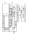
この公知例を用いた駆動回路として、従来技術のデータ線駆動回路81を図1に示す。データ線駆動回路81は、ロジック部88と、パネル3を駆動する駆動部89とを具備している。
ロジック部88において、表示メモリ(RAM)回路83には、1フレーム分以下の階調データが格納される。表示メモリ回路83は、信号処理回路82から供給されるアドレス制御信号により、RAMの1行分のアドレスを1番目から最終番目であるn番目まで選択し、上記選択されたn個のアドレスから、パネル3の1表示ライン分のn個の階調データを一斉に読み出してラッチ回路B16に出力する。ラッチ回路B16は、そのn個の階調データを保持し、信号処理回路82からのラッチクロックであるラッチ信号(STB信号)に応じて、上記n個の階調データを一斉にデータ演算回路84に出力する。
データ演算回路84は、n個の階調データに所定の論理演算処理を信号処理として施して、駆動部89のレベルシフト回路17を介してD/A変換回路18に出力する。所定の論理演算処理としては、極性反転処理POL、反転処理REV、全黒処理DISP0、全白処理DISP1の少なくとも1つの処理が挙げられ、信号処理回路82からの論理演算処理命令により指定される。極性反転処理POLは、液晶を交流駆動するために階調データを反転する処理である。反転処理REVは、映像表示を全く反対の色にする処理である。全黒または全白処理は、階調データに関わりなく黒または白の信号に変換する処理である。
駆動部89のD/A変換回路18は、諧調電圧生成回路19から供給される複数の階調電圧の中から、データ演算回路84からのn個の階調データのそれぞれに応じた所定の階調電圧を選択し、それぞれ、データ線Y1〜Ynを介して、パネル3の1表示ライン分の1番目からn番目までの画素に供給する。
As a driving circuit using this known example, a data
In the
The
The D /
しかしながら、ロジック部88では、表示メモリ回路83からパネル3の1表示ライン分の階調データを一斉に読み出してラッチ回路B16に出力している。また、表示メモリ回路83は、kビット×n個のセンスアンプを備えている。このため、データ演算回路84での階調データに対して論理演算処理を同時に行なうことと、kビット×n個のセンスアンプの動作電流により、ロジック部88での回路電流のピーク電流が大きくなり、電源回路から表示パネル3の共通電極に供給されるVcom電圧にもノイズが伝播してしまい、横縞やフリッカなどにより画質が悪化してしまう。
また、データ演算回路84は、1表示ライン分の階調データに対して一斉に極性反転処理などの論理演算処理を行なうため、データ演算回路84の回路規模が大きくなる。
However, the
In addition, since the
本発明の課題は、ノイズを低減して、画質を向上することができる表示装置の駆動回路を提供することにある。 An object of the present invention is to provide a driving circuit for a display device that can reduce noise and improve image quality.
以下に、[発明を実施するための最良の形態]で使用する番号・符号を用いて、課題を解決するための手段を説明する。これらの番号・符号は、[特許請求の範囲]の記載と[発明を実施するための最良の形態]の記載との対応関係を明らかにするために付加されたものであるが、[特許請求の範囲]に記載されている発明の技術的範囲の解釈に用いてはならない。 Hereinafter, means for solving the problem will be described using the numbers and symbols used in [Best Mode for Carrying Out the Invention]. These numbers and symbols are added to clarify the correspondence between the description of [Claims] and the description of [Best Mode for Carrying Out the Invention]. It should not be used to interpret the technical scope of the invention described in “
本発明の駆動回路は、複数の階調データを表示メモリ回路(13)からデータバス(21,22,23)を介して順番に読み出し、複数の前記読み出された階調データを表示画素データとして一括して出力するロジック部(8)と、前記ロジック部(8)から出力された前記表示画素データに基づいて生成されたアナログ階調信号で表示装置を駆動する駆動部(9)とを具備している。これにより、メモリ回路から階調データがp画素単位に読み出されるので、ロジック部で発生する過渡電流のピーク値を減少させ、ノイズを減らすことができる。 The drive circuit of the present invention sequentially reads a plurality of gradation data from the display memory circuit (13) via the data buses (21, 22, 23), and the plurality of the read gradation data are displayed as display pixel data. A logic unit (8) that collectively outputs the data and a drive unit (9) that drives the display device with an analog grayscale signal generated based on the display pixel data output from the logic unit (8). It has. As a result, gradation data is read from the memory circuit in units of p pixels, so that the peak value of the transient current generated in the logic unit can be reduced and noise can be reduced.
本発明により、駆動回路内部の過渡電流に起因するノイズを低減して、表示装置の画質を向上することができる。 According to the present invention, noise caused by a transient current in the drive circuit can be reduced and the image quality of the display device can be improved.
本発明によれば、ロジック部8では、メモリ13から表示装置の1表示ライン分の階調データを1番目からn番目まで分割して順番に読み出してバッファ回路20、データバス21、22,23、データ演算回路14,24、ラッチ回路A15を介してラッチ回路B16に出力する。これにより、センスアンプの数が1/nになるため動作電流も1/nに低減し、バッファ回路20、データ演算回路14,24、ラッチ回路A15が1表示ライン分の階調データに対して一斉に信号処理を施す場合に比べて、同時に信号処理を行なわない分、過渡電流のピーク値を減少させてノイズの発生量を低減して、安定したVcom電圧を電源回路11から表示装置の共通電極7に供給することができ、画質を向上することができる。
According to the present invention, the
この場合、データ演算回路14,24は、1表示ライン分の階調データに対して一斉に論理演算処理を行なう必要がなく、1表示ライン分の階調データを1番目からn番目まで順番に信号処理を行なっている。このため、データ演算回路14,24の回路規模を従来のデータ演算回路84よりも縮小することができる。
In this case, the
また、本発明によれば、ロジック部8では、データ演算回路14が多数決演算処理を行なうことにより、データバス22,23での充放電電力を低減することができる。
Further, according to the present invention, in the
また、本発明によれば、ロジック部8では、データ演算回路24が表示画素データを判別して不要な階調に対応するバッファアンプ部51のバイアス電流の供給を制御することにより、消費電力を削減することができる。
Further, according to the present invention, in the
以下に、本発明の表示装置の駆動回路について詳細に説明する。ただし、本発明は以下の実施形態に限定されるものではない。 Hereinafter, the drive circuit of the display device of the present invention will be described in detail. However, the present invention is not limited to the following embodiments.
[第1実施形態]
図2を参照して、本発明の第1実施形態による駆動回路を説明する。図2に示されるように、本発明の第1実施形態による駆動回路は、例えば、携帯電話機の表示装置に適用されることができる。この表示装置は、データ線駆動回路1、走査線駆動回路2,表示パネル3を備えている。また、データ線駆動回路1は表示メモリ(RAM)回路13を内蔵している。表示装置には、携帯電話機などのCPU(Central Processing Unit:図示せず)からデジタル信号が供給される。このデジタル信号には、各画素の色の濃淡を示す6ビットのデジタル階調信号(階調データ)や、表示メモリ回路13のどの領域に階調データを書き込むかを指定するアドレス制御信号や、コマンド信号や、スタンバイ信号などの制御信号が含まれる。
[First Embodiment]
With reference to FIG. 2, the driving circuit according to the first embodiment of the present invention will be described. As shown in FIG. 2, the drive circuit according to the first embodiment of the present invention can be applied to a display device of a mobile phone, for example. The display device includes a data
表示メモリ回路13は、1フレーム分の階調データを記憶する回路である。携帯電話機などに使用される表示装置の駆動回路では、データ線駆動回路1に表示メモリ回路13が設けられている。次のフレーム表示が現在のフレーム表示から変化しない時には、CPUから表示装置への次のフレームのデジタル信号の供給を止めることにより、CPUと表示装置とのインターフェイス部の消費電力が低減されている。また、次のフレーム表示の一部だけが現在のフレーム表示から変化する時には、変化する領域のアドレス制御信号と変化する部分に対応する階調データが供給される。これにより、CPUでの処理負担が軽減されている。この例では、表示メモリ回路13の記憶容量は、1フレーム分である例を説明するが、記憶容量は1フレーム以上でも、1フレーム以下でもよい。1フレーム以下の例としては、表示パネル3の一部分のみ表示するパーシャルメモリなどが知られている。
The
表示パネル3は、複数のデータ線4と、複数の走査線5と、マトリックス状に配置された画素6と、コモン電極線7とを備えている。画素6は、複数のデータ線4と複数の走査線5との交点の各々に設けられ、表示電極と、表示電極に対向する共通電極と、スイッチ素子であるTFT(Thin Film Transistor)とを含んでいる。TFTのドレインは、表示電極に接続され、そのゲートは走査線5に接続され、そのソースはデータ線4に接続されている。表示電極と共通電極の間には液晶層や有機EL層などが設けられている。共通電極は、コモン電極線7が接続されている。走査線駆動回路2は走査線5を順番に駆動する。データ線駆動回路1は、CPUからデジタル信号を受信して格納し、各走査線5が駆動されるとき、デジタル信号をアナログ階調信号に変換し、表示パネル3のデータ線4を介して画素6に一斉に供給される。これにより、表示パネル3全体に映像が表示される。
The display panel 3 includes a plurality of data lines 4, a plurality of
図3は、データ線駆動回路1の構成を示している。
データ線駆動回路1は、ロジック部8と、駆動部9と、電源回路11とを内蔵している。電源回路11は、ロジック部8と、駆動部9に接続されている。
FIG. 3 shows the configuration of the data line driving
The data line driving
電源回路11は、ロジック部8と駆動部9とに異なる電源電圧を供給する。例えば、ロジック部8、駆動部9に供給される電源電圧は、それぞれ3V以下、3V以上である。一般に集積回路では、3V以下の電源電圧が使用されているが、液晶表示装置の駆動電圧としては3V以上の電源電圧が必要である。また、携帯電話機では、電池から電源電圧が供給されているが、その供給される電圧(VDC)も3V以下であることが多い。そのため、駆動部9に供給される電源電圧を生成する電源回路が必要となる。
The
また、液晶表示装置においては、データ線4から画素6に印加される画素電圧の極性が、所定の期間ごとに反転される駆動方法が知られている。つまり、画素6が交流的に駆動される場合がある。ここで、極性とは、液晶の共通電極の電圧(Vcom電圧)を基準とした場合の画素電圧の正負を示す。このような駆動方法は、液晶材料の劣化を防止するために適用されている。この交流駆動方法として、Vcom電圧に直流電圧を印加し、データ線4に供給する正極及び負極のアナログ階調信号を1走査線ごと及びフレームごとに反転するドット反転駆動法や、また、別の駆動方法として、Vcom電圧が1走査線駆動ごとに反転されるコモン反転駆動法が知られている。いずれの場合にも、電源回路11は、Vcom電圧を生成する。
In the liquid crystal display device, a driving method is known in which the polarity of the pixel voltage applied from the data line 4 to the pixel 6 is inverted every predetermined period. That is, the pixel 6 may be driven in an alternating manner. Here, the polarity indicates the polarity of the pixel voltage when the voltage of the common electrode of the liquid crystal (Vcom voltage) is used as a reference. Such a driving method is applied to prevent deterioration of the liquid crystal material. As this AC driving method, a dot inversion driving method in which a DC voltage is applied to the Vcom voltage and the positive and negative analog gradation signals supplied to the data line 4 are inverted for each scanning line and for each frame, As a driving method, a common inversion driving method is known in which the Vcom voltage is inverted every one scanning line driving. In either case, the
電源回路11は、定電圧発生回路(図示せず)と、スイッチと容量で構成されるDCDCコンバータ回路(図示せず)とを備えている。定電圧発生回路には、上記のVDC電圧が供給され、一定の電圧を生成する。DCDCコンバータ回路は、その電圧に基づいて、システムグランド(SGND)に対するロジック電圧、駆動電圧、Vcom電圧を生成する。システムグランドは、電源回路11の共通電源であり、電源回路11、ロジック部8、駆動部9に供給される。ロジック電圧は、システムグランドに対して3V以下の電源電圧であり、ロジック部8に供給される。駆動電圧は、システムグランドに対して3V以上の電源電圧であり、駆動部9に供給される。Vcom電圧は、システムグランドに対するコモン電圧を表し、コモン電極線7に供給される。
The
このシステムグランド(SGND)や、定電圧発生回路にノイズが伝播すると、電源回路11から表示パネル3の共通電極に供給されるVcom電圧にもノイズが伝播してしまう。その結果、フリッカやクロストークなどにより画質が劣化する。このノイズは、駆動回路内部で発生し、デジタル信号の変化に応じてノイズのピーク値は増減する。ロジック部8、駆動部9でのノイズの発生を抑制するには、信号処理におけるピーク電流値を少なくすることが有効である。そのため、ロジック部8では、表示メモリ回路13から表示パネル3の1表示ライン分の階調データを一斉に読み出すのではなく、表示メモリ回路13から表示パネル3の1表示ライン分の階調データをp画素単位(p:自然数)に1番目から最終番目であるn番目(nは整数)まで分割して順番に読み出すのがよい。以降の説明では、R、G、Bの3画素を1単位、つまりp=3として説明する。
When noise propagates to the system ground (SGND) or the constant voltage generation circuit, the noise also propagates to the Vcom voltage supplied from the
ロジック部8について説明する。ロジック部8は、信号処理回路12、表示メモリ回路13、データ演算回路14、ラッチ回路A15、ラッチ回路B16、バッファ回路20、データバス21、22を備えている。
The
信号処理回路12は、ロジック部8、駆動部9内の各回路に接続されている。信号処理回路12は、CPUから供給されるデジタル信号を受信する。このデジタル信号には、各画素の階調を示す階調データと、コマンド信号と、アドレス制御信号と、論理演算処理命令とが含まれる。この例では、画素6に対応する階調データは、赤、緑、青に対して各6ビット(64階調)の18ビットで構成されている。コマンド信号は、表示メモリ回路13に対する書き込み命令又は読み出し命令を含んでいる。アドレス制御信号は、表示メモリ回路13に対する書き込み又は読み出しの開始アドレスを含んでいる。信号処理回路12は、これらの信号や、後述の水平クロック信号、垂直クロック信号などに基づいてメモリ制御信号を生成する。階調データとメモリ制御信号は表示メモリ回路13に供給されている。また、コマンド信号には、クロック周波数を設定するためのクロック周波数設定信号が含まれる。この場合、信号処理回路12は、発振回路(図示せず)を備え、その発振回路は、クロック周波数設定信号に基づいて、水平クロック信号(HCLK信号)、垂直クロック信号(VCLK信号)、水平スタート信号、垂直スタート信号、ラッチ信号(STB信号)などのクロック制御信号を生成する。信号処理回路12は、クロック制御信号を、データ線駆動回路1のロジック部8と駆動部9内の各回路と走査線駆動回路2に供給する。また、コマンド信号には、表示パネル3に画像を2値表示するための2値モード信号や、表示パネル3に同じ画像を表示するスタンバイモード信号、表示パネル3の一部分のみに画像を表示するパーシャル表示を行なうためのパーシャルモード信号が含まれる。信号処理回路12は、コマンド信号に基づいて動作モードを設定するためのモード制御信号を生成する。信号処理回路12は、モード制御信号を駆動部9のD/A変換回路18と階調電圧生成回路19に供給する。
The
表示メモリ回路13は、上述のように、1フレーム分の階調データを記憶する回路である。図4は、表示メモリ回路13の詳細を示している。図4に示されるように、表示メモリ回路13は、SRAMのようなRAM(Random Access Memory)30と、Yアドレスデコーダ35と、Xアドレスデコーダ36とを備えている。アドレスデコーダ35,36には、RAM30がアクセスされるときの初期画素アドレスが信号処理回路12により設定される。信号処理回路12からメモリ制御信号がXアドレスデコーダ36に供給されたとき、Xアドレスデコーダ36は、初期画素アドレスに基づいてRAM30の1行を指定する。また信号処理回路12からメモリ制御信号がYアドレスデコーダ35に供給されたとき、Yアドレスデコーダ35は、初期アドレスに基づいてRAM30の指定された行の指定された画素アドレス、一般的には1番目の画素アドレスを指定する。その後、信号処理回路12からメモリ制御信号がアドレスデコーダ35に供給される度に、Yアドレスデコーダ35は、RAM30の指定された行の画素アドレスを順に指定する。このとき、Yアドレスデコーダ35は、列アドレス信号C1〜Cnを出力する。
As described above, the
信号処理回路12からのメモリ制御信号に書き込み命令が含まれるとき、アドレスデコーダ35、36は、メモリ制御信号に応じて、RAM30のアドレスを順に選択する。選択されたアドレスに階調データが書き込まれる。こうして、RAM30は、表示パネル3の1フレーム分に対応する階調データを格納する。信号処理回路12からのメモリ制御信号に駆動部9への読み出し命令が含まれるとき、アドレスデコーダ35、36は、メモリ制御信号に応じて、RAM30の各行と各列のアドレスを順に選択する。選択されたアドレスから階調データが読み出される。読み出された階調データは、バッファ回路20に出力される。
When a write command is included in the memory control signal from the
バッファ回路20は、表示メモリ回路13から読み出された階調データをデータバス21あるいはラッチ回路A15に供給する。図4に示されるように、バッファ回路20は、センスアンプ31と、データバス32と、セレクタ部33と、遅延回路34とを備えている。データバス32は、各画素(R、B、Gの3画素を1単位とする画素)に対する18ビットの階調データに対応する18本の信号線を備えている。セレクタ部33は、1表示ラインの画素数をP画素単位(ここではR、B、Gの3画素を1単位とする)で分割した数分のセレクタ33−1〜33−nを含んでいる。各セレクタは、18個のスイッチを備えている。表示メモリ回路13からの列アドレス信号に応じて、各セレクタのスイッチは閉じられ、対応する画素の階調データは、データバス32に接続される。センスアンプ31は、データバス32に接続され、各画素(R、B、Gの3画素を1単位とする画素)に対する18ビットの階調データに対応するセンスアンプP0〜P17を含んでいる。このように、本発明の駆動回路では、センスアンプ31はR、B、Gの3画素を1単位とする1画素分設けられているだけであり、従って、従来技術では、表示メモリ回路13にビットごとにあったセンスアンプが大幅に低減されるので駆動回路を小型化することができる。センスアンプP0〜P17は、データバス32上の18ビットの階調データを増幅してデータバス21上に出力する。遅延回路34は、表示メモリ回路13からのアドレス信号Cj(1≦j≦n)を水平クロック周期だけ遅延させ、遅延したアドレス信号Ejをラッチ回路A15に供給する。即ち、遅延回路34は、表示メモリ回路13からのアドレス信号Cjを保持し、HCLK信号に応じて、そのアドレス信号Cjをサンプリング信号Ejとしてラッチ回路A15に出力する。
The
図4に示されるように、データバス21は、増幅された18ビットの階調データRAM_D(0:17)に対応して18本の信号線により構成されている。データバス22は、18ビットの表示画素データD(0:17)に対応する18本の信号線と、1ビット分の多数決信号(MAJ信号)に対応する1本の信号線との19本の信号線により構成されている。18ビットの表示画素データD(0:17)とMAJ信号は、表示画素データ&MAJ信号としてデータ演算回路14から出力される。
As shown in FIG. 4, the
図5は、データ演算回路14の詳細を示している。図5に示されるように、データ演算回路14は、論理回路37と、多数決演算回路38と、ラッチ回路39とを備えている。論理回路37と多数決演算回路38は、OR回路、AND回路、EXOR回路などの論理回路で実現できる。論理回路37は、バッファ回路20からの階調データRAM_D(0:17)に所定の論理演算処理を施して、多数決演算回路38に出力する。所定の論理演算処理としては、極性反転処理POL、反転処理REV、全黒処理DISP0、全白処理DISP1の少なくとも1つの処理が挙げられ、信号処理回路12からの論理演算処理命令により指定される。極性反転処理POLでは、液晶を交流駆動するために階調データがビット反転される。反転処理REVでは、映像表示を反対の色にする処理で、階調データがビット反転される。全黒または全白処理では、階調データに関わりなく黒または白の信号が出力される。多数決演算回路38は、論理回路37からの表示画素データD(0:17)に後述の多数決演算処理MAJを施して、後述の表示画素データD(0:17)と後述のMAJ信号とをラッチ回路39に出力する。ラッチ回路39は、多数決演算回路38からの表示画素データD(0:17)とMAJ信号とを水平クロック周期だけ遅延させてラッチ回路A15に供給する。即ち、ラッチ回路39は、多数決演算回路38からの表示画素データD(0:17)とMAJ信号とを保持し、HCLK信号に応じて、データバス22を介してラッチ回路A15に出力する。
データ演算回路14内の論理回路が処理する順番は、例えば、反転処理REV−全黒処理DISP0−全白処理DISP1−極性反転処理POL−多数決演算処理MAJである。このように、最後が極性反転処理POL−多数決演算処理MAJの順であれば他の論理回路を追加してもよい。
ここで、「階調データ」とは、表示メモリ回路13に格納されたデジタルの信号であって、階調データがデータ演算回路14や、ラッチ回路A15を介した信号は「表示画素データ」として区別する。
FIG. 5 shows details of the
The processing order of the logic circuit in the
Here, the “gradation data” is a digital signal stored in the
ラッチ回路A15は、データ演算回路14から表示画素データとMAJ信号がデータバス22に出力されたとき、MAJ信号と表示画素データD(0:17)の各ビットとのEXORを施す。即ち、ラッチ回路A15は、MAJ信号が表す非反転指示命令“0”に従って、表示画素データD(0:17)を反転しないで、そのまま保持する。MAJ信号が“1”のとき、ラッチ回路A15は、MAJ信号が表す反転指示命令“1”に従って、多数決演算処理MAJが施された表示画素データD(0:17)をビット反転して保持する。また、ラッチ回路A15には、バッファ回路20の遅延回路34からサンプリング信号Enが供給される。ラッチ回路A15は、保持している表示画素データを、サンプリング信号Enに応じて、ラッチ回路B16に出力する。
When the display pixel data and the MAJ signal are output from the data
多数決演算処理MAJについて説明する。多数決演算回路38は、前回の表示画素データD(0:17)をデータバス22から入力し、今回の表示画素データD(0:17)は、論理回路37から供給される。多数決演算回路38は、前回の18ビットの表示画素データD(0:17)と今回の18ビット分の表示画素データD(0:17)との間で多数決演算処理を実行する。多数決演算回路38は、前回の表示画素データD(0:17)のビットの各々と今回の表示画素データD(0:17)のビットのうち対応するビットとを比較し、今回の表示画素データD(0:17)で反転されたビットの数が過半数より多いか、少ないかを判定する。反転ビットの数が過半数より多い場合、多数決演算回路38は、前回の表示画素データD(0:17)のビットのうち、反転されていないビットに対応するビットを反転する。また、このとき多数決演算回路38は、ラッチ回路A15に対する反転指示命令“1”を表すMAJ信号を生成し、多数決演算処理MAJが施された表示画素データD(0:17)とMAJ信号“1”とをラッチ回路39に出力する。一方、反転ビットの数が過半数より少ない場合、多数決演算回路38は、ラッチ回路A15に対する非反転指示命令“0”を表すMAJ信号を生成し、今回の表示画素データD(0:17)とMAJ信号“0”とをラッチ回路39に出力する。ラッチ回路39は、水平クロック信号HCLKに同期して、多数決演算回路38からの表示画素データD(0:17)とMAJ信号“0”とを保持して、データバス22上に出力する。
The majority operation processing MAJ will be described. The majority decision operation circuit 38 receives the previous display pixel data D (0:17) from the
例として、表示画素データが4ビットで、データバス22に供給する信号を(表示画素データ4ビット;MAJ信号1ビット)として説明する。前回の表示画素データがa(0000)であり、今回の表示画素データがb(1101)である場合、表示画素データb(1101)のビットは、表示画素データa(0000)のビットと較べて、3ビット分0から1に変化している。上述のように、多数決演算により過半数より多く表示画素データのビットが変化している時には、多数決演算回路38は、表示画素データb(1101)のビットのうち、表示画素データa(0000)のビットと較べて反転されていないビットを反転して、表示画素データb’(0010)を生成する。同時に、MAJ信号を“1”に設定する。表示画素データb’(0010)とMAJ信号“1”とを表示画素データ&MAJ信号(0010;1)としてラッチ回路39を介してデータバス22に出力する。ラッチ回路A15では、データバス22に供給された表示画素データ&MAJ信号(0010;1)を受け取ったとき、MAJ信号“1”に従って、表示画素データb’(0010)を反転し、表示画素データb(1101)を保持する。これにより、多数決演算処理MAJが施されない場合は3個のビットが反転するが、多数決演算処理MAJが施された場合は、MAJ信号を含めて2個のビットを反転するだけなので、データバス22での充放電電力が低減される。
As an example, the display pixel data is 4 bits, and the signal supplied to the
表示画素データを構成するビットが偶数個である場合は、変化するビットが同数になる時がある。その時は、MAJ信号が変化しないように処理する。例として、表示メモリ回路13からデータバス21に供給される階調データがa(0000)→b(1100)→c(0011)→d(1010)と変化する場合、多数決演算回路38は、a’(0000;0)→b’(1100;0)→c’(1100;1)→d’(0101;1)の表示画素データ&MAJ信号をラッチ回路39を介してデータバス22に供給する。a→bで、階調データを構成するビットのうちの2個のビットが変化しているが、a’のMAJ信号が“0”なので、b’でもMAJ信号は“0”として階調データはビット反転されない。c→dでも2個のビットが変化しているが、c’のMAJ信号が“1”なので、MAJ信号は“1”として、階調データをビット反転する。
When there are an even number of bits constituting the display pixel data, the number of changing bits may be the same. At that time, processing is performed so that the MAJ signal does not change. As an example, when the gradation data supplied from the
ラッチ回路A15において、サンプリング信号がシフトレジスタ回路で生成され、階調データが順番にラッチされるシリアル転送方式比べ、アドレス制御方式では、デコーダが必要となる。例えば、256本×3(RGB)のデータ線4を駆動するには、8ビットのデコーダが必要で、8ビットのデコーダはシフトレジスタ回路より回路規模が大きい。しかし、本発明では、表示メモリ回路13のアドレスデコーダ35、36がそのデコーダとして兼用されているので、回路規模の増大が抑制されている。アドレス制御方式は、走査線駆動回路2に適用してもよい。パーシャル表示のオフ表示領域では飛び越し走査を行い、また、同時に複数の走査線5を活性化することもできる。
In the latch circuit A15, a decoder is required in the address control method as compared with the serial transfer method in which the sampling signal is generated by the shift register circuit and the grayscale data is sequentially latched. For example, in order to drive 256 × 3 (RGB) data lines 4, an 8-bit decoder is required, and the 8-bit decoder has a larger circuit scale than the shift register circuit. However, in the present invention, since the
ラッチ回路B16は、ラッチ回路A15からの表示画素データを保持し、信号処理回路12からのラッチ信号(STB信号)に応じて、保持されている表示画素データを一斉に駆動部9に出力する。
The latch circuit B16 holds the display pixel data from the latch circuit A15, and outputs the held display pixel data all at once to the
次に、駆動部9について説明する。駆動部9は、レベルシフト回路17、D/A変換回路18、階調電圧生成回路19を備えている。
Next, the
レベルシフト回路17は、ラッチ回路B16とD/A変換回路18と階調電圧生成回路19に接続されている。レベルシフト回路17は、ラッチ回路B16からの表示画素データの電圧レベルをロジック電圧レベルから駆動電圧レベルに変換する。
The
図6に示されるように、階調電圧生成回路19は、スイッチ41と、抵抗分圧回路42と、第1基準電圧V0を供給する第1バッファアンプと、第2基準電圧V63を供給する第2バッファアンプとを備えている。抵抗分圧回路42は、直列接続された63個の抵抗素子r0〜r62を備えている。スイッチ41の一端は、第1基準電圧V0に接続されている。スイッチ41の他端は、抵抗素子r0の一端が接続されている。抵抗素子r62の一端は、第2基準電圧V63に接続されている。第1基準電圧V0又は第2基準電圧V63を指定する2値モード信号やスタンバイ信号を含むモード制御信号が供給されない場合、つまり、通常駆動モードでは、スイッチ41はオンしている。この場合、抵抗分圧回路42は、2個の基準電圧V0、V63を、ガンマ特性に適合するように63個の抵抗素子r0〜r62により分圧し、64個の異なる階調電圧を生成する。ここで、基準電圧はV0とV63の2個と簡略したが、V0とV63以外の複数の基準電圧を設けて抵抗分圧回路42に供給してよい。上記のモード制御信号が供給された場合、つまり、低消費電力駆動モードでは、スイッチ41はオフされ、抵抗分圧回路42に流れる電流が遮断され、消費電力を低減している。
As shown in FIG. 6, the grayscale
上述のように、ロジック部8は、電源回路11から供給されるロジック電圧により動作し、駆動部9は、電源回路11から供給される駆動電圧により動作する。このように、ロジック部8と駆動部9との電圧レベルが異なる。このため、レベルシフト回路17は、ラッチ回路B16からの表示画素データの電圧レベルをロジック電圧から駆動電圧に変換する。
As described above, the
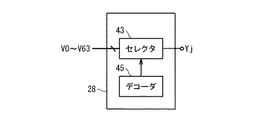
D/A変換回路18は、表示画素データを、アナログ階調信号に変換する。このD/A変換回路18は、1表示ライン分の3×n個のD/Aコンバータを含んでいる。3×n個のD/Aコンバータの各々は、図7に示されるように、セレクタ43と、バッファアンプ44と、デコーダ45と、スイッチ46、48、49とを備えている。デコーダ45は、レベルシフト回路17に接続されている。セレクタ43は、階調電圧生成回路19とデコーダ45とに接続されている。バッファアンプ44は、その入力にセレクタ43が接続され、その出力にスイッチ46の一端が接続されている。スイッチ46の他端には、データ線4であるデータ線Yj(1≦j≦3n)が接続されている。また、このD/A変換回路18は、n個のD/Aコンバータで構成され、3時分割にデータ線Yj(1≦j≦3n)を駆動してもよい。この場合、D/A変換回路18とデータ線4との間に時分割スイッチ(図示なし)を設け、表示メモリ回路13からは1画素分ずつの階調データを転送する。
上記のモード制御信号が供給されない通常駆動モードでは、スイッチ46はオンし、スイッチ48、49はオフしている。この場合、デコーダ45は、ラッチ回路B16からレベルシフト回路17を介して供給される表示画素データをデコードしてセレクタ43に出力する。セレクタ43は、階調電圧生成回路19から供給される64個の階調電圧の中から、デコーダ45からの表示画素データに応じた所定の階調電圧を選択する。バッファアンプ44は、選択された階調電圧を、データ線Yjを介して、表示パネル3の所定の画素6に供給する。
2値モード信号を含むモード制御信号が供給された低消費電力駆動モードでは、スイッチ46はオフしてバッファアンプ44のバイアス電流を遮断し、スイッチ48又はスイッチ49はオンして基準電圧(V0、V63)を、データ線Yjを介して、表示パネル3の所定の画素6に供給する。
The D /
In the normal drive mode in which the mode control signal is not supplied, the
In the low power consumption driving mode supplied with the mode control signal including the binary mode signal, the
なお、D/A変換回路18のバッファアンプの利得(出力信号/入力信号の比)を1より大きくするなどして、複数の階調電圧(V0からV63)を利得倍にすれば、レベルシフト回路17を省略することができる。
また、データ線駆動回路1は、表示画素データを、D/A変換回路18によりアナログ階調電圧に変換しているが、上記のD/A変換回路18に代えて、表示画素データに基づいてアナログ階調電流を生成する回路を用いてもよい。
If the gain (output signal / input signal ratio) of the buffer amplifier of the D /
The data line driving
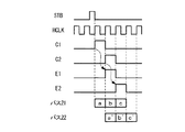
図8は、本発明の第1実施形態1による表示装置の動作を示すタイミングチャートである。 FIG. 8 is a timing chart showing the operation of the display device according to the first embodiment of the present invention.
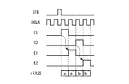
いま、表示メモリ回路13のRAM30に、表示パネル3の1フレーム分に対応する階調データが格納されているとする。信号処理回路12は、STB信号をラッチ回路B16に出力した後、読み出し命令を含むメモリ制御信号を表示メモリ回路13に供給する。このとき、表示メモリ回路13のアドレスデコーダ35、36は、信号処理回路12から供給されるメモリ制御信号に応答して、RAM30の1行分のアドレスを1番目からn番目までこの順に選択し、それぞれ上記選択されたn個のアドレスを表すn個のアドレス信号C1〜Cnをこの順でバッファ回路20に出力する。RAM30は、上記選択されたn個のアドレスのそれぞれから、表示パネル3の1表示ライン分の1番目からn番目までの画素6に対応するn個の階調データa、b、c、...をこの順にバッファ回路20に出力する。バッファ回路20は、n個の階調データa、b、c、...を1番目からn番目までこの順でデータバス21に順番に供給する。また、バッファ回路20は、n個のアドレス信号C1〜Cnをこの順に保持し、所定クロック(HCLK信号)分だけ遅延して、n個のサンプリング信号E1〜Enとして順番にラッチ回路A15に出力する。 データ演算回路14は、n個の階調データa、b、c、...に対してこの順に論理演算処理と多数決演算処理MAJとを施し、所定クロック(HCLK信号)分だけ遅延して、n個の表示画素データa’、b’、c’,...をこの順でデータバス22に供給する。ここで、第(j−1)表示画素データの各ビットと較べて、第j表示画素データの対応するビットが、反転されているとき、その反転ビットの数が過半数より多い場合、データ演算回路14は、第j表示画素データのビットのうちの反転されていないビットに対応する第(j−1)表示画素データのビットを反転する多数決演算処理MAJが実行され、第j表示画素データとして反転された第(j−1)表示画素データと、ラッチ回路A15に対する反転指示命令“1”を表すMAJ信号とをデータバス22に供給する。ラッチ回路A15は、データバス22に供給されたn個の表示画素データa’、b’、c’,...をこの順で保持し、所定クロック(それぞれn個のサンプリング信号E1〜En)分だけ遅延して、上記n個の表示画素データa’、b’、c’,...をこの順にラッチ回路B16に出力する。ここで、ラッチ回路A15は、MAJ信号“1”に従って、多数決演算処理MAJが施された第j表示画素データを反転して保持し、所定クロック(サンプリング信号Ej)分だけ遅延して、ラッチ回路B16に出力する。ラッチ回路B16は、ラッチ回路A15からのn個の表示画素データa’、b’、c’,...をこの順で保持し、信号処理回路12からのSTB信号に応じて、上記n個の表示画素データa’、b’、c’,...を一斉に駆動部9に出力する。
駆動部9のD/A変換回路18は、諧調電圧生成回路19から供給される64個の階調電圧の中から、ラッチ回路B16からのn個の表示画素データa’、b’、c’,...のそれぞれに応じた所定の階調電圧を選択し、それぞれ、データ線Y1〜Y3nを介して、表示パネル3の1表示ライン分の1番目から3n番目までの所定の画素6に供給する。
Now, it is assumed that gradation data corresponding to one frame of the display panel 3 is stored in the
The D /
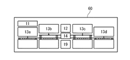
上記の駆動回路は、同一の基板(チップ)に集積化されている。データ線駆動回路1をシリコンなどの半導体基板に集積化した例を図9、図10に示す。図9に示される集積回路60では、データ演算回路14、電源回路11、信号処理回路12、階調電圧生成回路19が集積回路60の1箇所に配置されている。また、表示メモリ回路13は、表示メモリ回路13a、13b、13c、13dの4ブロックに分割されて集積回路60に配置されている。図示しないが、バッファ回路20、ラッチ回路A15、ラッチ回路B16、レベルシフト回路17、D/A変換回路18は、表示メモリ回路13a、13b、13c、13dのそれぞれに対応するように、4ブロックに分割されて集積回路60に配置されている。また、データバス21、22は、表示メモリ回路13a、13b、13c、13dのそれぞれに対応するように、4ブロックに分割されて集積回路60に配置され、データ演算回路14に接続されている。また、表示メモリ回路13を4ブロックに分割することで、1表示ラインを4つに分割したときの階調データを同時にデータ演算回路14で処理している。
The above drive circuit is integrated on the same substrate (chip). An example in which the data
図10に示される集積回路61では、上記の集積回路60に対して、データ演算回路14を集積回路61の2箇所に配置している。即ち、データ演算回路14をデータ演算回路14x、14yとした場合、データ演算回路14xは、データバス21、22の4ブロックのうち、表示メモリ回路13a、13bに対応する2ブロックに接続され、データ演算回路14yは、データバス21、22の4ブロックのうち、表示メモリ回路13c、13dに対応する2ブロックに接続されている。これにより、データバス21、22の配線長が短くなり配線容量が減少し、データバス21、22での充放電電力が低減される。
In the
このように、集積化して、部分数を減らすことで表示装置としての信頼性は向上する。 In this manner, reliability as a display device is improved by integrating and reducing the number of parts.
以上説明したように、本発明によれば、ロジック部8では、表示メモリ回路13から表示パネル3の1表示ライン分の階調データを一斉に読み出してラッチ回路B16に出力するのではなく、表示メモリ回路13から表示パネル3の1表示ライン分の階調データを1番目からn番目まで分割して順番に読み出し、バッファ回路20、データバス21、22、データ演算回路14、ラッチ回路A15を介してラッチ回路B16に出力する。これにより、センスアンプの数が1/nになるため動作電流も1/nに低減し、バッファ回路20、データ演算回路14、ラッチ回路A15が1表示ライン分の階調データに対して一斉に信号処理を施す場合に比べて、同時に信号処理を行なわない分、過渡電流が減少し、ノイズの発生量を低減して、安定したVcom電圧を電源回路11から表示パネル3の共通電極に供給することができ、画質を向上することができる。この場合、データ演算回路14は、1表示ライン分の階調データに対して一斉に論理演算処理を行なう必要がなく、1表示ライン分の階調データを1番目からn番目まで順番に信号処理(論理演算処理、多数決演算処理)を行なっている。このため、データ演算回路14の回路規模を従来のデータ演算回路84よりも縮小することができる。
As described above, according to the present invention, the
また、本発明によれば、ロジック部8では、データ演算回路14が多数決演算処理を行なうことにより、データバス22での充放電電力を削減することができる。
Further, according to the present invention, in the
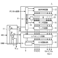
[第2実施形態]
次に、本発明の第2実施形態による駆動回路について説明する。第1実施形態と同じ内容については説明を割愛し、異なる点のみを説明する。図11は第2実施形態による表示装置の駆動回路の構成を示すブロック図である。第1実施形態ではデータバス21、22の2グループあったのに対し、第2実施形態では、1つのデータバス23が提供され、データバスは共有されている。つまり、表示メモリ回路13からの階調データは、バッファ回路20でデータバス23を介してデータ演算回路14に供給され、データ演算回路14で所定の信号処理を行った表示画素データもデータバス23を介してデータラッチ回路A15に供給される。バッファ回路20とデータ演算回路14の出力がぶつからないように、交互にデータバス23を共有する。センスアンプ31とデータバス23との間、データ演算回路14の出力部とデータバス23との間には、切替スイッチ(図示なし)が設けられる。切替スイッチは、信号処理回路12からのHCLK信号に応じて、センスアンプ31とデータバス23とを接続する第1接続モードと、データ演算回路14の出力部とデータバス23とを接続する第2接続モードとを交互に実行する。第1実施形態に比べデータ転送能力は半減するが、データバスの本数が削減できる。
[Second Embodiment]
Next, a drive circuit according to a second embodiment of the present invention will be described. Description of the same contents as in the first embodiment will be omitted, and only different points will be described. FIG. 11 is a block diagram showing the configuration of the drive circuit of the display device according to the second embodiment. In the first embodiment, there are two groups of
図12はデータバスを共有するためのタイミングチャートを示す。表示メモリ13からの階調データaはアドレス信号C1に応じて選択され、選択された階調データは、第1接続モードにおいて、センスアンプ31およびデータバス23を介してデータ演算回路14に供給される。データ演算回路14で所定の信号処理が行なわれた表示画素データa’は、第2接続モードにおいて、1クロック周期遅れたサンプリング信号E1に応じて、データバス23を介してラッチ回路A15に供給される。
FIG. 12 shows a timing chart for sharing the data bus. The gradation data a from the
[第3実施形態]
次に、本発明の第3実施形態による駆動回路について説明する。第1実施形態と同じ内容については説明を割愛し、異なる点のみを説明する。図13は第3実施形態の表示装置の駆動回路の構成を示すブロック図である。第1実施形態との相違点は、ロジック部8は、データ演算回路14に代えてデータ演算回路24を備え、更に、判別信号バス25を備えている点である。駆動部9は、階調電圧生成回路19に代えて階調電圧生成回路26を備え、D/A変換回路18に代えてD/A変換回路28を備えている。
[Third Embodiment]
Next, a driving circuit according to a third embodiment of the present invention will be described. Description of the same contents as in the first embodiment will be omitted, and only different points will be described. FIG. 13 is a block diagram showing the configuration of the drive circuit of the display device of the third embodiment. The difference from the first embodiment is that the
図14に示されるように、データ演算回路24には、上記のデータ演算回路14の構成に加えて、データ判別回路50が論理回路37と多数決演算回路38との間に設けられている。データ判別回路50は、表示画素データの各ビットを判別し、その判別結果を表す判別信号を、判定信号バス25を介して出力する。判定信号バス25は、表示画素データが6ビットの場合では64本の信号から成り、64本の信号の各々を表示画素データに基づいて活性または非活性にする。
階調電圧生成回路26には、図15に示されるように、上記の階調電圧生成回路19の構成に加えて、バイアス電圧制御回路52と、バッファアンプ部51が設けられている。バッファアンプ部51は、基準電圧V0とV63以外の複数の階調電圧のそれぞれに対して複数のバッファアンプを有するバッファアンプ部51が設けられている。バイアス電圧制御回路52は、データ判別回路50からの64本の信号に基づいて、バッファアンプ部51の複数のバッファアンプの各々のバイアス電流を制御する。即ち、62個のバッファアンプは、それぞれ、活性時に、抵抗分圧回路42により生成される62個の階調電圧V1〜V62を出力する。
D/A変換回路28では、図16に示されるように、D/A変換回路18と較べてバッファアンプ44、スイッチ46、48、49が削除されている。
As shown in FIG. 14, in the
As shown in FIG. 15, the gradation
In the D /
データ判別回路50は、論理回路37からの表示画素データを判別して、判別信号を判定信号バス25に出力する。例えば、判別信号が、任意の1水平期間の全データ線に黒表示を行なうことを表している場合、バイアス電圧制御回路52は、判別信号に従って、バッファアンプ部51の複数のバッファアンプのうち、0階調電圧に対応するバッファアンプのみ活性化し、その他(1階調から63階調)の階調電圧に対応するバッファアンプを非活性とする。中間階調である階調電圧V31のみの表示では、階調電圧V0、V63、V31に対応するバッファアンプのみを活性にし、他の階調電圧(V1〜V30、V32からV62)に対応するバッファアンプは非活性とする。階調電圧V0、V63以外の階調電圧は、階調電圧V0、V63を基準に階調電圧を生成しているので、階調電圧V0、V63に対応するバッファアンプは全黒表示、全白表示以外では活性状態にする。これにより、表示に必要のない階調電圧に対応するバッファアンプのバイアス電流を遮断することにより、消費電力を削減することができる。
The data discrimination circuit 50 discriminates display pixel data from the
[第4実施形態]
次に本発明の第4実施形態による駆動回路について説明する。第1実施形態と同じ内容については説明を割愛し、異なる点のみを説明する。図17は、第4実施形態の表示装置の駆動回路の構成を示すブロック図である。第1実施形態との相違点は、ロジック部8が、バッファ回路20に代えてバッファ回路27を備え、更に、バッファ回路27と表示メモリ回路13との間にシフトレジスタ回路29を備えていることにある。
[Fourth Embodiment]
Next explained is a drive circuit according to the fourth embodiment of the invention. Description of the same contents as in the first embodiment will be omitted, and only different points will be described. FIG. 17 is a block diagram illustrating a configuration of a drive circuit of the display device according to the fourth embodiment. The difference from the first embodiment is that the
図18に示されるように、バッファ回路27では、上記のバッファ回路20と較べて遅延回路34が削除され、代わりに、シフトレジスタ回路29がロジック部8に設けられている。
信号処理回路12からシフトレジスタ回路29に上記のHCLK信号とスタート信号が供給される。この場合、シフトレジスタ回路29は、HCLK信号とスタート信号に応じて、Yアドレスデコーダ35の出力をサンプリング信号Fjとしてラッチし、ラッチ回路A15と表示メモリ回路13のセレクタ部のセレクタ33−jとに順番に出力する。この例では、データラッチ回路A15への表示画素データの入力のサンプリング信号は、表示メモリ回路13からの階調データの読み出しのサンプリング信号から1クロック周期分遅延しており、表示メモリ回路13からの階調データの読み出しのサンプリング信号はF1、F2、…、Fnとし、データラッチ回路A15への表示画素データの入力のサンプリング信号は、F2、F3、…、F(n+1)とする。遅延するクロック数は、データ演算回路14により行なわれる演算処理に応じて決定される。
As shown in FIG. 18, in the
The HCLK signal and the start signal are supplied from the
以上、本発明について説明したが、上記実施形態はその矛盾が生じない範囲で任意に組み合わせることが可能である。本発明の駆動回路を含む集積回路は、シリコンなどの半導体基板以外にも、ガラスやプラスチックなど他の基板に集積化されてもよい。また、上記では、表示画素データが6ビット(64階調)で説明したが、表示画素データは5ビット以下でも、7ビット以上でもよい。また、主に液晶表示装置について説明したが、有機EL表示装置など他の表示装置についても適用できる。 Although the present invention has been described above, the above-described embodiments can be arbitrarily combined within a range in which the contradiction does not occur. The integrated circuit including the driving circuit of the present invention may be integrated on another substrate such as glass or plastic in addition to a semiconductor substrate such as silicon. In the above description, the display pixel data is 6 bits (64 gradations), but the display pixel data may be 5 bits or less or 7 bits or more. Although the liquid crystal display device has been mainly described, the present invention can also be applied to other display devices such as an organic EL display device.
1、81 データ線駆動回路
2 走査線駆動回路
3 パネル
4 データ線
5 走査線
6 画素
7 コモン電極線
8、88 ロジック部
9、89 駆動部
11 電源回路
12、82 信号処理回路
13、83 表示メモリ回路
14、24、84 データ演算回路
15、16、39 ラッチ回路
17 レベルシフト回路
18、28 D/A変換回路
19、26 階調電圧生成回路
20、27 バッファ回路
21、22、23、25、32 データバス
29 シフトレジスタ回路
30 RAM
31、44、51 バッファアンプ
33、41、43、46、48、49 スイッチ
34 遅延回路
35、36、45 デコーダ
37 論理処理回路
38 多数決演算回路
42 抵抗分圧回路
50 データ判別回路
52 バイアス電圧制御回路
60、61 集積回路
DESCRIPTION OF
31, 44, 51
Claims (7)
前記ロジック部から出力された前記複数の表示画素データに基づいて生成された複数のアナログ階調信号を、表示装置の複数のデータ線に出力する駆動部と
を具備し、
前記ロジック部は、
前記表示メモリ回路と前記データバスとの間に設けられ、前記表示メモリ回路から読み出された前記複数の階調データを、p画素単位の階調データ(p:前記表示装置のデータ線総数よりも少ない自然数)として前記データバスに出力するp画素分のセンスアンプと、
前記データバスに接続され、前記p画素分のセンスアンプから出力された前記p画素単位の階調データに演算処理を行い、第1表示画素データとしてラッチ回路に出力するデータ演算回路と
を具備する
表示装置の駆動回路。 A logic unit that sequentially reads a plurality of gradation data from a display memory circuit via a data bus, and outputs the read plurality of gradation data as a plurality of display pixel data;
A drive unit that outputs a plurality of analog gradation signals generated based on the plurality of display pixel data output from the logic unit to a plurality of data lines of a display device;
The logic part is
The plurality of gradation data provided between the display memory circuit and the data bus and read from the display memory circuit are converted into gradation data in p pixel units (p: total number of data lines of the display device) A sense amplifier for p pixels to be output to the data bus as a small natural number)
A data operation circuit that is connected to the data bus, performs arithmetic processing on the grayscale data in units of p pixels output from the sense amplifier for the p pixels, and outputs to the latch circuit as first display pixel data. A driving circuit of a display device.
前記ロジック部と前記駆動部とに第1と第2の電源電圧のうちの少なくとも一方を供給する電源回路
を更に具備し、
前記ロジック部と、前記駆動部と、前記電源回路は同一半導体チップ内に形成されている
表示装置の駆動回路。 In the display device drive circuit according to claim 1,
A power supply circuit for supplying at least one of a first power supply voltage and a second power supply voltage to the logic unit and the driving unit;
The logic unit, the driving unit, and the power supply circuit are formed in the same semiconductor chip.
前記駆動部は、
前記ロジック部から出力された前記複数の表示画素データの電圧レベルを変換するためのレベルシフト回路と、
所定数の階調電圧を発生する階調電圧発生回路と、
前記複数のデータ線の各々に対して設けられ、前記レベルシフト回路から出力された前記複数の表示画素データに基づいて前記所定数の階調電圧のうちの1つを選択し、選択された階調電圧に基づいて前記表示装置の1つのデータ線を駆動する複数のD/Aコンバータを有するD/A変換回路と
を具備する
表示装置の駆動回路。 The drive circuit of the display device according to claim 1 or 2,
The drive unit is
A level shift circuit for converting voltage levels of the plurality of display pixel data output from the logic unit;
A gradation voltage generating circuit for generating a predetermined number of gradation voltages;
One of the predetermined number of gradation voltages is selected based on the plurality of display pixel data provided for each of the plurality of data lines and output from the level shift circuit, and the selected level is selected. And a D / A conversion circuit having a plurality of D / A converters for driving one data line of the display device based on a regulated voltage.
前記階調電圧発生回路は、
少なくとも2つの基準電圧と、
前記基準電圧を分圧するための抵抗分圧回路と
を具備する
表示装置の駆動回路。 In the display device drive circuit according to claim 3,
The gradation voltage generation circuit includes:
At least two reference voltages;
A drive circuit for a display device, comprising: a resistance voltage dividing circuit for dividing the reference voltage.
前記階調電圧発生回路は、
少なくとも2つの基準電圧と、
前記基準電圧を分圧するための抵抗分圧回路と、
前記抵抗分圧回路の出力を増幅するためのバッファアンプ群と、
前記複数の表示画素データに対応する、前記選択された階調電圧のそれぞれが出力されるように、前記データ演算回路で生成される判別信号に基づいて、前記バッファアンプ群のいずれかを活性化するバイアス電圧制御回路と
を具備する
表示装置の駆動回路。 In the display device drive circuit according to claim 3,
The gradation voltage generation circuit includes:
At least two reference voltages;
A resistance voltage dividing circuit for dividing the reference voltage;
A buffer amplifier group for amplifying the output of the resistance voltage dividing circuit;
One of the buffer amplifier groups is activated based on a determination signal generated by the data arithmetic circuit so that each of the selected gradation voltages corresponding to the plurality of display pixel data is output. And a bias voltage control circuit for driving the display device.
前記複数のD/Aコンバータの各々は、
前記レベルシフト回路から出力された前記複数の表示画素データをデコードするデコーダと、
前記デコーダから出力されるデコード結果に従って前記所定数の階調電圧のうちの1つを選択して、前記表示装置の1つのデータ線に供給するセレクタと
を具備する
表示装置の駆動回路。 The drive circuit of the display device according to claim 3,
Each of the plurality of D / A converters includes:
A decoder for decoding the plurality of display pixel data output from the level shift circuit;
A display device driving circuit comprising: a selector that selects one of the predetermined number of gradation voltages according to a decoding result output from the decoder and supplies the selected one to one data line of the display device.
前記複数の表示画素データに基づいて生成された複数のアナログ階調信号を表示装置の複数のデータ線に出力する第2のステップと
を具備し、
前記第1のステップは、
前記表示メモリ回路の前記複数の階調データを、p画素単位の階調データ(p:前記表示装置のデータ線総数よりも少ない自然数)としてp画素分のセンスアンプに出力するステップと、
前記p画素分のセンスアンプから出力された前記p画素単位の階調データに演算処理を行い、第1表示画素データとして出力するステップと、
順番に出力された前記第1表示画素データのそれぞれを保持して、前記複数の表示画素データとして一括して出力するステップと
を備える
表示装置の駆動方法。 A first step of sequentially reading a plurality of gradation data from the display memory circuit, and outputting the read plurality of gradation data as a plurality of display pixel data;
A second step of outputting a plurality of analog gradation signals generated based on the plurality of display pixel data to a plurality of data lines of a display device;
The first step includes
Outputting the plurality of gradation data of the display memory circuit to a p-pixel sense amplifier as p-pixel gradation data (p: a natural number smaller than the total number of data lines of the display device);
Performing arithmetic processing on the grayscale data in units of p pixels output from the sense amplifier for the p pixels, and outputting as first display pixel data;
A step of holding each of the first display pixel data output in order and outputting the first display pixel data collectively as the plurality of display pixel data.
Priority Applications (3)
| Application Number | Priority Date | Filing Date | Title |
|---|---|---|---|
| JP2005150024A JP4942012B2 (en) | 2005-05-23 | 2005-05-23 | Display device drive circuit and drive method |
| US11/437,609 US20060262059A1 (en) | 2005-05-23 | 2006-05-22 | Drive circuit for display apparatus and driving method |
| CNA2006100848641A CN1870119A (en) | 2005-05-23 | 2006-05-23 | Drive circuit for display apparatus and driving method |
Applications Claiming Priority (1)
| Application Number | Priority Date | Filing Date | Title |
|---|---|---|---|
| JP2005150024A JP4942012B2 (en) | 2005-05-23 | 2005-05-23 | Display device drive circuit and drive method |
Publications (2)
| Publication Number | Publication Date |
|---|---|
| JP2006330101A JP2006330101A (en) | 2006-12-07 |
| JP4942012B2 true JP4942012B2 (en) | 2012-05-30 |
Family
ID=37443768
Family Applications (1)
| Application Number | Title | Priority Date | Filing Date |
|---|---|---|---|
| JP2005150024A Expired - Fee Related JP4942012B2 (en) | 2005-05-23 | 2005-05-23 | Display device drive circuit and drive method |
Country Status (3)
| Country | Link |
|---|---|
| US (1) | US20060262059A1 (en) |
| JP (1) | JP4942012B2 (en) |
| CN (1) | CN1870119A (en) |
Families Citing this family (16)
| Publication number | Priority date | Publication date | Assignee | Title |
|---|---|---|---|---|
| JP2007328255A (en) * | 2006-06-09 | 2007-12-20 | Futaba Corp | Active matrix type display element |
| JP2008009170A (en) * | 2006-06-29 | 2008-01-17 | Toshiba Matsushita Display Technology Co Ltd | Liquid crystal display device and driving method of liquid crystal display device |
| KR100805547B1 (en) * | 2006-11-14 | 2008-02-20 | 삼성에스디아이 주식회사 | OLED display and driving method thereof |
| JP5046226B2 (en) | 2007-04-02 | 2012-10-10 | 株式会社ジャパンディスプレイウェスト | Image display device |
| US20100060621A1 (en) * | 2008-09-10 | 2010-03-11 | Himax Technologies Limited | Source driver device and display device having the same |
| JP5138096B2 (en) * | 2009-05-22 | 2013-02-06 | シャープ株式会社 | Image display device |
| KR101056303B1 (en) * | 2009-10-12 | 2011-08-11 | 삼성모바일디스플레이주식회사 | Organic light emitting display device and driving method thereof |
| KR101093258B1 (en) * | 2009-11-12 | 2011-12-14 | 삼성모바일디스플레이주식회사 | LCD Display |
| KR101897011B1 (en) * | 2010-11-30 | 2018-09-10 | 엘지디스플레이 주식회사 | Liquid crystal display appratus and method for driving the same |
| KR101469480B1 (en) * | 2012-04-05 | 2014-12-12 | 엘지디스플레이 주식회사 | Display device and method for driving the saem |
| KR101962781B1 (en) * | 2012-07-12 | 2019-07-31 | 삼성전자주식회사 | Display driving circuit and electronic device comprising the same |
| JP6320679B2 (en) * | 2013-03-22 | 2018-05-09 | セイコーエプソン株式会社 | LATCH CIRCUIT FOR DISPLAY DEVICE, DISPLAY DEVICE, AND ELECTRONIC DEVICE |
| US10102792B2 (en) * | 2016-03-30 | 2018-10-16 | Novatek Microelectronics Corp. | Driving circuit of display panel and display apparatus using the same |
| CN105957489B (en) * | 2016-07-08 | 2018-10-26 | 东莞市健耀烨电子科技有限公司 | A kind of method and realization method for checking specific fan-shaped display area |
| CN110070827B (en) * | 2019-05-22 | 2023-05-23 | 富满微电子集团股份有限公司 | LED display screen driving chip, latch signal generation method and system |
| CN116097657B (en) | 2021-08-31 | 2026-01-13 | 京东方科技集团股份有限公司 | Display device, image signal processing device, acquisition device and display system |
Family Cites Families (32)
| Publication number | Priority date | Publication date | Assignee | Title |
|---|---|---|---|---|
| US4503291A (en) * | 1982-11-12 | 1985-03-05 | Dasa Corporation | Repertory dialer with efficient data storage |
| JPS59180871A (en) * | 1983-03-31 | 1984-10-15 | Fujitsu Ltd | Semiconductor memory device |
| JP2504571B2 (en) * | 1989-08-04 | 1996-06-05 | 富士通株式会社 | Semiconductor integrated circuit device |
| FR2669448B1 (en) * | 1990-11-19 | 1993-01-15 | Bull Sa | TERMINAL ARCHITECTURE AND MANAGEMENT CIRCUIT. |
| JPH0535200A (en) * | 1991-07-31 | 1993-02-12 | Hitachi Ltd | Display device and driving method thereof |
| JPH0695617A (en) * | 1992-09-14 | 1994-04-08 | Hitachi Ltd | Liquid crystal display device and display controller |
| JP3579461B2 (en) * | 1993-10-15 | 2004-10-20 | 株式会社ルネサステクノロジ | Data processing system and data processing device |
| US5805126A (en) * | 1994-05-05 | 1998-09-08 | Neomagic Corporation | Display system with highly linear, flicker-free gray scales using high framecounts |
| JP3395866B2 (en) * | 1995-04-12 | 2003-04-14 | シャープ株式会社 | Liquid crystal drive |
| JP3436478B2 (en) * | 1998-01-12 | 2003-08-11 | 株式会社日立製作所 | Liquid crystal display device and computer system |
| JP3258283B2 (en) * | 1998-11-05 | 2002-02-18 | インターナショナル・ビジネス・マシーンズ・コーポレーション | Data transfer method and apparatus for reducing data change amount |
| US6373478B1 (en) * | 1999-03-26 | 2002-04-16 | Rockwell Collins, Inc. | Liquid crystal display driver supporting a large number of gray-scale values |
| EP1146501B1 (en) * | 1999-10-18 | 2011-03-30 | Seiko Epson Corporation | Display device with memory integrated on the display substrate |
| JP3964593B2 (en) * | 2000-02-24 | 2007-08-22 | 富士通株式会社 | Semiconductor memory device |
| JP3494366B2 (en) * | 2000-08-04 | 2004-02-09 | 松下電器産業株式会社 | DA converter |
| JP3759394B2 (en) * | 2000-09-29 | 2006-03-22 | 株式会社東芝 | Liquid crystal drive circuit and load drive circuit |
| JP3501751B2 (en) * | 2000-11-20 | 2004-03-02 | Nec液晶テクノロジー株式会社 | Driving circuit for color liquid crystal display and display device provided with the circuit |
| EP1207622B1 (en) * | 2000-11-21 | 2013-02-27 | Omron Corporation | Semiconductor relay system |
| JP3533187B2 (en) * | 2001-01-19 | 2004-05-31 | Necエレクトロニクス株式会社 | Driving method of color liquid crystal display, circuit thereof, and portable electronic device |
| KR100456987B1 (en) * | 2001-04-10 | 2004-11-10 | 가부시키가이샤 히타치세이사쿠쇼 | Display device and display driving device for displaying display data |
| JP4743570B2 (en) * | 2001-04-10 | 2011-08-10 | ルネサスエレクトロニクス株式会社 | Semiconductor integrated circuit with built-in power supply circuit, liquid crystal display control device, and portable electronic device |
| JP3744827B2 (en) * | 2001-05-02 | 2006-02-15 | セイコーエプソン株式会社 | Semiconductor device, display device, display panel, and electronic device |
| EP1431952A4 (en) * | 2001-09-28 | 2009-12-02 | Sony Corp | DISPLAY MEMORY, ATTACK CIRCUIT, DISPLAY SCREEN, AND CELL INFORMATION APPARATUS |
| US6882329B2 (en) * | 2001-09-28 | 2005-04-19 | Canon Kabushiki Kaisha | Drive signal generator and image display apparatus |
| JP3807321B2 (en) * | 2002-02-08 | 2006-08-09 | セイコーエプソン株式会社 | Reference voltage generation circuit, display drive circuit, display device, and reference voltage generation method |
| US6788282B2 (en) * | 2002-02-21 | 2004-09-07 | Seiko Epson Corporation | Driving method for electro-optical device, driving circuit therefor, electro-optical device, and electronic apparatus |
| US6901027B2 (en) * | 2002-04-30 | 2005-05-31 | Sony Corporation | Apparatus for processing data, memory bank used therefor, semiconductor device, and method for reading out pixel data |
| JP4019851B2 (en) * | 2002-08-06 | 2007-12-12 | 松下電器産業株式会社 | Current drive |
| JP2004233743A (en) * | 2003-01-31 | 2004-08-19 | Renesas Technology Corp | Electronic device having display drive control device and display device |
| JP4516280B2 (en) * | 2003-03-10 | 2010-08-04 | ルネサスエレクトロニクス株式会社 | Display device drive circuit |
| US6975535B2 (en) * | 2003-08-14 | 2005-12-13 | Mosel Vitelic, Inc. | Electronic memory, such as flash EPROM, with bitwise-adjusted writing current or/and voltage |
| JP4744074B2 (en) * | 2003-12-01 | 2011-08-10 | ルネサスエレクトロニクス株式会社 | Display memory circuit and display controller |
-
2005
- 2005-05-23 JP JP2005150024A patent/JP4942012B2/en not_active Expired - Fee Related
-
2006
- 2006-05-22 US US11/437,609 patent/US20060262059A1/en not_active Abandoned
- 2006-05-23 CN CNA2006100848641A patent/CN1870119A/en active Pending
Also Published As
| Publication number | Publication date |
|---|---|
| CN1870119A (en) | 2006-11-29 |
| US20060262059A1 (en) | 2006-11-23 |
| JP2006330101A (en) | 2006-12-07 |
Similar Documents
| Publication | Publication Date | Title |
|---|---|---|
| US8111230B2 (en) | Drive circuit of display apparatus | |
| JP4942012B2 (en) | Display device drive circuit and drive method | |
| CN100444218C (en) | Display driver and electro-optical device | |
| JP4492334B2 (en) | Display device and portable terminal | |
| US8044911B2 (en) | Source driving circuit and liquid crystal display apparatus including the same | |
| US20080316234A1 (en) | Method of driving electro-optical device, source driver, electro-optical device, projection-type display device, and electronic instrument | |
| JP4810840B2 (en) | Reference voltage generation circuit, display driver, electro-optical device, and electronic apparatus | |
| US20060181494A1 (en) | Reference voltage generation circuit, display driver, electro-optical device, and electronic instrument | |
| US7616183B2 (en) | Source driving circuit of display device and source driving method thereof | |
| JP2008225494A (en) | Display driver and electro-optical device | |
| US20060198009A1 (en) | Reference voltage generation circuit, display driver, electro-optical device, and electronic instrument | |
| US20060181544A1 (en) | Reference voltage select circuit, reference voltage generation circuit, display driver, electro-optical device, and electronic instrument | |
| JP2006243233A (en) | Reference voltage generation circuit, display driver, electro-optical device, and electronic apparatus | |
| US7471278B2 (en) | Display driver, electro-optical device, and drive method | |
| US20070008265A1 (en) | Driver circuit, electro-optical device, and electronic instrument | |
| US20070139349A1 (en) | Driving ic for a display device | |
| JP4371038B2 (en) | Data driver, electro-optical device, electronic apparatus, and driving method | |
| JP5119901B2 (en) | Source driver, electro-optical device, projection display device, and electronic device | |
| JP5235048B2 (en) | Display device, electronic equipment | |
| CN100449600C (en) | Drive circuit, image display device and portable device provided with same | |
| JP4947167B2 (en) | Display device and portable terminal | |
| JP2007183670A (en) | Reference voltage generation circuit, display driver, electro-optical device, and electronic apparatus | |
| JP2007171997A (en) | Reference voltage generation circuit, display driver, electro-optical device, and electronic apparatus |
Legal Events
| Date | Code | Title | Description |
|---|---|---|---|
| A621 | Written request for application examination |
Free format text: JAPANESE INTERMEDIATE CODE: A621 Effective date: 20080411 |
|
| A977 | Report on retrieval |
Free format text: JAPANESE INTERMEDIATE CODE: A971007 Effective date: 20110408 |
|
| A131 | Notification of reasons for refusal |
Free format text: JAPANESE INTERMEDIATE CODE: A131 Effective date: 20110509 |
|
| A521 | Request for written amendment filed |
Free format text: JAPANESE INTERMEDIATE CODE: A523 Effective date: 20110705 |
|
| A131 | Notification of reasons for refusal |
Free format text: JAPANESE INTERMEDIATE CODE: A131 Effective date: 20111212 |
|
| A521 | Request for written amendment filed |
Free format text: JAPANESE INTERMEDIATE CODE: A523 Effective date: 20120208 |
|
| TRDD | Decision of grant or rejection written | ||
| A01 | Written decision to grant a patent or to grant a registration (utility model) |
Free format text: JAPANESE INTERMEDIATE CODE: A01 Effective date: 20120223 |
|
| A01 | Written decision to grant a patent or to grant a registration (utility model) |
Free format text: JAPANESE INTERMEDIATE CODE: A01 |
|
| A61 | First payment of annual fees (during grant procedure) |
Free format text: JAPANESE INTERMEDIATE CODE: A61 Effective date: 20120223 |
|
| R150 | Certificate of patent or registration of utility model |
Free format text: JAPANESE INTERMEDIATE CODE: R150 |
|
| FPAY | Renewal fee payment (event date is renewal date of database) |
Free format text: PAYMENT UNTIL: 20150309 Year of fee payment: 3 |
|
| S531 | Written request for registration of change of domicile |
Free format text: JAPANESE INTERMEDIATE CODE: R313531 |
|
| R350 | Written notification of registration of transfer |
Free format text: JAPANESE INTERMEDIATE CODE: R350 |
|
| LAPS | Cancellation because of no payment of annual fees |