EP1457960A2 - Ansteuerverfahren für einen Plasmabildschirm - Google Patents
Ansteuerverfahren für einen Plasmabildschirm Download PDFInfo
- Publication number
- EP1457960A2 EP1457960A2 EP04075718A EP04075718A EP1457960A2 EP 1457960 A2 EP1457960 A2 EP 1457960A2 EP 04075718 A EP04075718 A EP 04075718A EP 04075718 A EP04075718 A EP 04075718A EP 1457960 A2 EP1457960 A2 EP 1457960A2
- Authority
- EP
- European Patent Office
- Prior art keywords
- period
- frame
- field
- sub
- selective
- Prior art date
- Legal status (The legal status is an assumption and is not a legal conclusion. Google has not performed a legal analysis and makes no representation as to the accuracy of the status listed.)
- Withdrawn
Links
Images



Classifications
-
- G—PHYSICS
- G09—EDUCATION; CRYPTOGRAPHY; DISPLAY; ADVERTISING; SEALS
- G09G—ARRANGEMENTS OR CIRCUITS FOR CONTROL OF INDICATING DEVICES USING STATIC MEANS TO PRESENT VARIABLE INFORMATION
- G09G3/00—Control arrangements or circuits, of interest only in connection with visual indicators other than cathode-ray tubes
- G09G3/20—Control arrangements or circuits, of interest only in connection with visual indicators other than cathode-ray tubes for presentation of an assembly of a number of characters, e.g. a page, by composing the assembly by combination of individual elements arranged in a matrix no fixed position being assigned to or needed to be assigned to the individual characters or partial characters
- G09G3/22—Control arrangements or circuits, of interest only in connection with visual indicators other than cathode-ray tubes for presentation of an assembly of a number of characters, e.g. a page, by composing the assembly by combination of individual elements arranged in a matrix no fixed position being assigned to or needed to be assigned to the individual characters or partial characters using controlled light sources
- G09G3/28—Control arrangements or circuits, of interest only in connection with visual indicators other than cathode-ray tubes for presentation of an assembly of a number of characters, e.g. a page, by composing the assembly by combination of individual elements arranged in a matrix no fixed position being assigned to or needed to be assigned to the individual characters or partial characters using controlled light sources using luminous gas-discharge panels, e.g. plasma panels
- G09G3/288—Control arrangements or circuits, of interest only in connection with visual indicators other than cathode-ray tubes for presentation of an assembly of a number of characters, e.g. a page, by composing the assembly by combination of individual elements arranged in a matrix no fixed position being assigned to or needed to be assigned to the individual characters or partial characters using controlled light sources using luminous gas-discharge panels, e.g. plasma panels using AC panels
- G09G3/291—Control arrangements or circuits, of interest only in connection with visual indicators other than cathode-ray tubes for presentation of an assembly of a number of characters, e.g. a page, by composing the assembly by combination of individual elements arranged in a matrix no fixed position being assigned to or needed to be assigned to the individual characters or partial characters using controlled light sources using luminous gas-discharge panels, e.g. plasma panels using AC panels controlling the gas discharge to control a cell condition, e.g. by means of specific pulse shapes
-
- G—PHYSICS
- G09—EDUCATION; CRYPTOGRAPHY; DISPLAY; ADVERTISING; SEALS
- G09G—ARRANGEMENTS OR CIRCUITS FOR CONTROL OF INDICATING DEVICES USING STATIC MEANS TO PRESENT VARIABLE INFORMATION
- G09G3/00—Control arrangements or circuits, of interest only in connection with visual indicators other than cathode-ray tubes
- G09G3/20—Control arrangements or circuits, of interest only in connection with visual indicators other than cathode-ray tubes for presentation of an assembly of a number of characters, e.g. a page, by composing the assembly by combination of individual elements arranged in a matrix no fixed position being assigned to or needed to be assigned to the individual characters or partial characters
- G09G3/22—Control arrangements or circuits, of interest only in connection with visual indicators other than cathode-ray tubes for presentation of an assembly of a number of characters, e.g. a page, by composing the assembly by combination of individual elements arranged in a matrix no fixed position being assigned to or needed to be assigned to the individual characters or partial characters using controlled light sources
- G09G3/28—Control arrangements or circuits, of interest only in connection with visual indicators other than cathode-ray tubes for presentation of an assembly of a number of characters, e.g. a page, by composing the assembly by combination of individual elements arranged in a matrix no fixed position being assigned to or needed to be assigned to the individual characters or partial characters using controlled light sources using luminous gas-discharge panels, e.g. plasma panels
- G09G3/288—Control arrangements or circuits, of interest only in connection with visual indicators other than cathode-ray tubes for presentation of an assembly of a number of characters, e.g. a page, by composing the assembly by combination of individual elements arranged in a matrix no fixed position being assigned to or needed to be assigned to the individual characters or partial characters using controlled light sources using luminous gas-discharge panels, e.g. plasma panels using AC panels
- G09G3/291—Control arrangements or circuits, of interest only in connection with visual indicators other than cathode-ray tubes for presentation of an assembly of a number of characters, e.g. a page, by composing the assembly by combination of individual elements arranged in a matrix no fixed position being assigned to or needed to be assigned to the individual characters or partial characters using controlled light sources using luminous gas-discharge panels, e.g. plasma panels using AC panels controlling the gas discharge to control a cell condition, e.g. by means of specific pulse shapes
- G09G3/294—Control arrangements or circuits, of interest only in connection with visual indicators other than cathode-ray tubes for presentation of an assembly of a number of characters, e.g. a page, by composing the assembly by combination of individual elements arranged in a matrix no fixed position being assigned to or needed to be assigned to the individual characters or partial characters using controlled light sources using luminous gas-discharge panels, e.g. plasma panels using AC panels controlling the gas discharge to control a cell condition, e.g. by means of specific pulse shapes for lighting or sustain discharge
- G09G3/2944—Control arrangements or circuits, of interest only in connection with visual indicators other than cathode-ray tubes for presentation of an assembly of a number of characters, e.g. a page, by composing the assembly by combination of individual elements arranged in a matrix no fixed position being assigned to or needed to be assigned to the individual characters or partial characters using controlled light sources using luminous gas-discharge panels, e.g. plasma panels using AC panels controlling the gas discharge to control a cell condition, e.g. by means of specific pulse shapes for lighting or sustain discharge by varying the frequency of sustain pulses or the number of sustain pulses proportionally in each subfield of the whole frame
-
- G—PHYSICS
- G09—EDUCATION; CRYPTOGRAPHY; DISPLAY; ADVERTISING; SEALS
- G09G—ARRANGEMENTS OR CIRCUITS FOR CONTROL OF INDICATING DEVICES USING STATIC MEANS TO PRESENT VARIABLE INFORMATION
- G09G3/00—Control arrangements or circuits, of interest only in connection with visual indicators other than cathode-ray tubes
- G09G3/20—Control arrangements or circuits, of interest only in connection with visual indicators other than cathode-ray tubes for presentation of an assembly of a number of characters, e.g. a page, by composing the assembly by combination of individual elements arranged in a matrix no fixed position being assigned to or needed to be assigned to the individual characters or partial characters
- G09G3/22—Control arrangements or circuits, of interest only in connection with visual indicators other than cathode-ray tubes for presentation of an assembly of a number of characters, e.g. a page, by composing the assembly by combination of individual elements arranged in a matrix no fixed position being assigned to or needed to be assigned to the individual characters or partial characters using controlled light sources
- G09G3/28—Control arrangements or circuits, of interest only in connection with visual indicators other than cathode-ray tubes for presentation of an assembly of a number of characters, e.g. a page, by composing the assembly by combination of individual elements arranged in a matrix no fixed position being assigned to or needed to be assigned to the individual characters or partial characters using controlled light sources using luminous gas-discharge panels, e.g. plasma panels
- G09G3/288—Control arrangements or circuits, of interest only in connection with visual indicators other than cathode-ray tubes for presentation of an assembly of a number of characters, e.g. a page, by composing the assembly by combination of individual elements arranged in a matrix no fixed position being assigned to or needed to be assigned to the individual characters or partial characters using controlled light sources using luminous gas-discharge panels, e.g. plasma panels using AC panels
- G09G3/296—Driving circuits for producing the waveforms applied to the driving electrodes
-
- G—PHYSICS
- G09—EDUCATION; CRYPTOGRAPHY; DISPLAY; ADVERTISING; SEALS
- G09G—ARRANGEMENTS OR CIRCUITS FOR CONTROL OF INDICATING DEVICES USING STATIC MEANS TO PRESENT VARIABLE INFORMATION
- G09G2310/00—Command of the display device
- G09G2310/06—Details of flat display driving waveforms
- G09G2310/065—Waveforms comprising zero voltage phase or pause
-
- G—PHYSICS
- G09—EDUCATION; CRYPTOGRAPHY; DISPLAY; ADVERTISING; SEALS
- G09G—ARRANGEMENTS OR CIRCUITS FOR CONTROL OF INDICATING DEVICES USING STATIC MEANS TO PRESENT VARIABLE INFORMATION
- G09G2320/00—Control of display operating conditions
- G09G2320/02—Improving the quality of display appearance
- G09G2320/0247—Flicker reduction other than flicker reduction circuits used for single beam cathode-ray tubes
-
- G—PHYSICS
- G09—EDUCATION; CRYPTOGRAPHY; DISPLAY; ADVERTISING; SEALS
- G09G—ARRANGEMENTS OR CIRCUITS FOR CONTROL OF INDICATING DEVICES USING STATIC MEANS TO PRESENT VARIABLE INFORMATION
- G09G2360/00—Aspects of the architecture of display systems
- G09G2360/16—Calculation or use of calculated indices related to luminance levels in display data
-
- G—PHYSICS
- G09—EDUCATION; CRYPTOGRAPHY; DISPLAY; ADVERTISING; SEALS
- G09G—ARRANGEMENTS OR CIRCUITS FOR CONTROL OF INDICATING DEVICES USING STATIC MEANS TO PRESENT VARIABLE INFORMATION
- G09G3/00—Control arrangements or circuits, of interest only in connection with visual indicators other than cathode-ray tubes
- G09G3/20—Control arrangements or circuits, of interest only in connection with visual indicators other than cathode-ray tubes for presentation of an assembly of a number of characters, e.g. a page, by composing the assembly by combination of individual elements arranged in a matrix no fixed position being assigned to or needed to be assigned to the individual characters or partial characters
- G09G3/2007—Display of intermediate tones
- G09G3/2018—Display of intermediate tones by time modulation using two or more time intervals
- G09G3/2022—Display of intermediate tones by time modulation using two or more time intervals using sub-frames
- G09G3/2025—Display of intermediate tones by time modulation using two or more time intervals using sub-frames the sub-frames having all the same time duration
Definitions
- the present invention relates to a plasma display panel, and more particularly, to a driving method of a plasma display panel for improving a picture quality.
- Plasma display panel (hereinafter referred to as "PDP") generally displays an image including character or graphic by generating light from fluorescent substance using ultraviolet rays with a wavelength of 147 nm, which is generated during a gas discharge of an inert mixture gas, such as He+Xe, Ne+Xe, He+Ne+Xe or the like.
- This PDP has easy slimness and large-sized characteristics, and provides a greatly improved picture quality thanks to the recent technology development.
- three-electrode alternating current (AC) surface discharge type PDP has advantages of a low voltage operation and a long life since wall charges stored on a surface in the course of discharge protect electrodes from sputtering generated by the discharge.
- AC alternating current
- FIG. 1 is a view illustrating a discharge cell of a conventional three-electrode AC surface discharge type plasma display panel.
- a discharge cell of the three-electrode AC surface discharge type PDP includes a scan electrode (Y) and a sustain electrode (Z) formed on an upper substrate 10, and an address electrode (X) formed on a lower substrate 18.
- Each of the scan electrode (Y) and the sustain electrode (Z) includes transparent electrodes 12Y and 12Z and metal bus electrodes 13Y and 13Z having line widths narrower than line widths of the transparent electrodes 12Y and 12Z formed at one-sided edge regions of the transparent electrodes 12Y and 12Z.
- the transparent electrodes 12Y and 12Z are generally formed of Indium-Tin-Oxide (hereinafter, referred to as 'ITO') on the upper substrate 10.
- the metal bus electrodes 13Y and 13Z are generally formed of chrome (Cr) on the transparent electrodes 12Y and 12Z to function to reduce a voltage drop caused by the transparent electrodes 12Y and 12Z having high resistance.
- An upper dielectric layer 14 and a passivation film 16 are layered on the upper substrate 10 having the scan electrode (Y) and the sustain electrode (Z) formed in parallel with each other. The wall charge generated at the time of plasma discharge is stored in the upper dielectric layer 14.
- the passivation film 16 prevents the upper dielectric layer 14 from being damaged due to the sputtering generating at the time of the plasma discharge and also, enhances an emission efficiency of a secondary electron.
- Magnesium oxide (MgO) is generally used as the passivation film 16.
- a lower dielectric layer 22 and a barrier 24 are formed on the lower substrate 18 having the address electrode (X), and a fluorescent layer 26 is coated on a surface of the lower dielectric layer 22 and the barrier 24.
- the address electrode (X) is formed in a direction of crossing with the scan electrode (Y) and the sustain electrode (Z).
- the barrier 24 is formed in parallel with the address electrode (X) to prevent the visible ray and the ultraviolet ray caused by the discharge from being leaked to an adjacent discharge cell.
- the fluorescent layer 26 is excited by the ultraviolet ray generated due to the plasma discharge to radiate any one visible ray of red, green or blue.
- the inert mixture gas for the discharge such as He+Xe, Ne+Xe, He+Ne+Xe and the like is injected into a discharge space of the discharge cell provided between the upper/lower substrates 10 and 18 and the barrier 24.
- one frame is divided into several sub-fields having different times of light-emitting (for example, the number of a sustain pulse) so as to realize a gray level of the image.
- Each of the sub-fields is again divided into a reset period during which the discharge is uniformly generated, an address period during which the discharge cell is selected, and the sustain period during which the gray level is embodied depending on discharge times.
- a frame period (16.67ms) corresponding to 1/60 second is divided into eight sub-fields (SF1 to SF8).
- each of the eight sub-fields (SF1 to SF8) is again divided into a reset period, an address period and a sustain period.
- brightness weighting values different from one another every sub-field are combined to embody a certain gray level.
- the conventional PDP can control the number of the sustain pulse depending on an Average Picture Level (hereinafter, referred to as "APL") such that a consumption power can be constantly processed.
- APL Average Picture Level
- FIG. 3 is a general graph illustrating the number of the sustain pulse depending on the APL.
- the PDP since brightness is determined depending on the number of the sustain pulse, if a total number of the sustain pulse is made identical in cases that an average brightness is dark and bright, the PDP has several drawbacks of a picture quality deterioration, a power consumption, a panel damage and the like. For example, a contrast is decreased in case that the number of the sustain pulse is set to be small for all inputted images. Further, in case that the number of the sustain pulse is set to be large for all inputted images, the PDP has an advantage in that the brightness is bright and the contrast is increased even at a dark image, but the panel can be damaged due to an increased consumption power and an elevated temperature of the panel.
- the number of the sustain pulse is abruptly increased in a range of gray level having a relative low APL, and is decreased in a range of gray level having a relative high APL. Accordingly, the number of the sustain pulse is abruptly varied in the range of gray level having the relative low APL.
- FIG. 4 is a view illustrating a voltage waveform representing a conventional driving method of the PDP.
- the sub-field (SF) included in one frame of the PDP is divided for an operation into the reset period (RPD), the address period (APD) and the sustain period (SPD).
- a reset pulse (RP) is supplied to the scan electrode (Y) during the reset period (RPD).
- the reset pulse (RP) having a ramp wave format is in a way of increasing voltage during a set-up period and decreasing the voltage during a set-down period.
- a plurality of minute set-up discharges is generated to form the wall charge in the upper dielectric layer.
- unnecessary charged particles are partially removed due to a plurality of minute set-down charges such that the wall charge is decreased as much as a next address discharge is helped without an erroneous discharge.
- a positive-polar (+) direct-current voltage is supplied to the sustain electrode (Z) during the set-down period.
- the scan electrode (Y) Since the reset pulse (RP) is supplied gradually attenuating with respect to the positive-polar (+) direct-current voltage, the scan electrode (Y) has a relative negative polarity (-) with respect to the sustain electrode (Z), that is, polarity is inverted at the time of set-down thereby causing the wall charges generated at the time of set-up to be decreased.
- a scan pulse (SP) having a negative-polar (-) scan voltage (Vy) is supplied to the scan electrode (Y) and at the same time, a positive-polar (+) data pulse (DP) is supplied to the address electrode (X) thereby causing the address discharge.
- SP scan pulse
- DP positive-polar (+) data pulse
- a triggering pulse is supplied to the scan electrode (Y) such that a sustain discharge is initiated at the discharge cells where enough wall charges are formed during the address period (APD).
- sustain pulses SUSPz and SUSPy
- Vs sustain voltage
- an erase pulse (EP) is supplied to the sustain electrode (Z) thereby stopping the maintained discharge.
- the erase pulse has the ramp wave format to provide small-sized light-emitting, or a short pulse width of about 1 ⁇ s for a discharge erase.
- the charged particles are erased using a short erase discharge caused by the erase pulse (EP), to thereby stop the discharge.
- two frames of FIGs. 6A and 6B be alternatively arranged every vertical synchronous signal.
- the sub-fields are arranged at an odd frame (or an even frame) in a weighted value ratio of 1, 6, 13, 23, 35, 51, 70, 91, 116, 145, 176 and 211 as in FIG. 6A, and the sub-fields are arranged at the even frame (or the odd frame) in a weighted value ratio of 4, 9, 18, 29, 43, 60, 80, 103, 130, 160, 193 and 109 as in FIG. 6B.
- an expression degree of the gray level can be increased at least twice as much as the case where the frames having the same brightness weighting value of each sub-field are arranged.
- the brightness weighting values of the sub-field should be set to be alternated each other every frame.
- the brightness weighting values of the odd frame and the even frame can be set to be alternated such as 1, 4, 6, 9, 13, 18, 23, 29 and the like.
- the brightness weighting value is alternatively arranged every frame as described above, there is a drawback in that light-emitting centers of each frame are inconsistent, and a flicker is generated to an extent of being unpleasant to the eye thereby deteriorating the picture quality. That is, when all sub-fields of each frame are turned-on, a light-emitting center of an odd numbered frame is a 211 position of the brightness weighting value, whileas a light-emitting center of an even numbered frame is a 193 position of the brightness weighting value. Accordingly, the positions of the light-emitting centers of both frames are different from each other thereby causing the flicker and accordingly, critically influencing the picture quality.
- VFB vertical frame blank
- one frame is comprised of at least one selective write sub-field and at least one selective erase sub-field.
- FIG. 7 is a view illustrating a waveform representing a conventional driving method of a selective write and selective erase PDP driven in a 60Hz mode.
- one frame of the selective write and selective erase PDP is comprised of at least one selective write sub-field and at least one selective erase sub-field.
- the at least one selective write sub-field can be a selective write duration (SW6 and the like)
- the at least one selective erase sub-field can be a selective erase duration (SE1, SE2 and the like).
- the selective write sub-field is divided into a reset period (RPD), an address period (APD), and a sustain period (SPD), and the selective erase sub-field is divided into an address period (APD) and a sustain period (SPD).
- RPD reset period
- APD address period
- SPD sustain period
- a set-down waveform ramp pulse (-RP) is sequentially supplied during the reset period (RPD) of the selective write sub-field to scan electrode lines (Y) following a set-up waveform reset pulse (RP).
- the set-down waveform ramp pulse (-RP) drops to a negative-polar (-) scan reference voltage (-Vw). Further, a positive-polar (+) direct-current voltage is supplied to sustain electrode lines (Z).
- a negative-polar (-) selective write scan pulse (SWSP) and a positive-polar (+) selective write data pulse (SWDP) are supplied to each of the scan electrode lines (Y) and the address electrode lines (X) to be synchronized with each other.
- sustain pulses (SUSPy and SUSPz) are alternatively supplied to the scan electrode lines (Y) and the sustain electrode lines (Z) such that the sustain discharge is generated at a cell turned-on by the address discharge of the selective write sub-field during the sustain period (SPD) of the selective write sub-field.
- the reset period (RPD) of the selective erase sub-field is omitted.
- a negative-polar (-) selective erase scan pulse (SESP) and a positive-polar (+) selective erase data pulse (SEDP) are supplied to each of the scan electrode lines (Y) and the address electrode lines (X) to be synchronized with each other.
- the selective erase scan pulse (SESP) drops to a negative-polar (-) selective erase scan voltage (Ve) higher than the negative-polar (-) scan reference voltage (Vw).
- the sustain pulses (SUSPy and SUSPz) are alternatively supplied to the scan electrode lines (Y) and the sustain electrode lines (Z) such that the sustain discharge is generated at cells not turned-off by the address discharge of the selective erase sub-field (ESF) during the sustain period (SPD) of the selective erase sub-field.
- the sustain pulse (SUSPy) having a relatively large pulse width is supplied to the scan electrode lines (Y) at the end time of a present selective erase sub-field.
- an erase pulse (not shown) and a ramp signal (not shown) are supplied to the scan electrode lines (Y) and the sustain electrode lines (Z) at the last selective erase sub-field having the selective write sub-field as the next sub-field to erase the sustain discharge of the turned-on cells.
- FIG. 8 is a view illustrating an example of a sub-field arrangement where the gray level is expressed in a selective write and selective erase way of FIG. 7.
- the sub-field from a low gray level to a first 32 gray level is addressed in a selective write way, and remaining sub-fields are addressed in a selective erase way.
- the flicker is caused by a phenomenon of a relative VFB increase (that is, VFB*(vertical frame blank at the time of a 60Hz driving) ⁇ VFB** (vertical frame blank at the time of the 50Hz driving)).
- VFB* vertical frame blank at the time of a 60Hz driving
- VFB** vertical frame blank at the time of the 50Hz driving
- the 60Hz mode that is, the frame period (16.67ms) corresponding 1/60 second.
- Europe, China and the like use a 50Hz mode, that is, a frame period (20ms) corresponding to 1/50 second.
- the VFB period is VFB*.
- the VFB period is VFB** longer than the case of 60Hz.
- the present invention is directed to a driving method of a plasma display panel that substantially obviates one or more problems due to limitations and disadvantages of the related art.
- An object of the present invention is to provide a driving method of a plasma display panel in which light-emitting centers coincide with one another every frame to improve a picture quality.
- a driving method of a plasma display panel characterized in that one frame period of the n th frame or the (n+1) th frame is variably set such that a brightness expression period can be identically set at the n th frame and the (n+1) th frame.
- each of the n th frame and the (n+1) th frame can include: a reset period during which a uniform wall charge is formed at a discharge cell; an address period during which an address discharge is generated to select the discharge cell; and a sustain period during which a sustain discharge is generated in the discharge cell where the address discharge is generated at predetermined times depending on a gray level value.
- the frame period can be varied by the address period or the sustain period.
- the address period varying the frame period can be varied by increase or decrease of a first period during which the wall charge formed during the address period is maintained.
- the sustain period varying the frame period can be varied by increase or decrease of a second period during which the wall charge formed during the sustain period is maintained.
- address period and the sustain period may be differently varied depending on an average picture level (APL).
- APL average picture level
- the frame period is varied by both of the address period and the sustain period.
- a driving method of a plasma display panel characterized in that one frame period of the selective write and selective erase frame driven in the 60Hz mode or the selective write and selective erase frame driven in the 50Hz mode is variably set such that a brightness expression period can be identically set at the selective write and selective erase frame driven in the 60Hz mode and the selective write and selective erase frame driven in the 50Hz mode.
- each of the selective write and selective erase frame driven in the 60Hz mode and the selective write and selective erase frame driven in the 50Hz mode can include: at least one selective write sub-field having a reset period during which a uniform wall charge is formed at a discharge cell, an address period during which an address discharge is generated to select the discharge cell, and a sustain period during which a sustain discharge is generated in the discharge cell where the address discharge is generated at predetermined times depending on a gray level value; and at least one selective erase sub-field having an address period during which an address discharge is generated to select the discharge cell, and a sustain period during which a sustain discharge is generated at predetermined times depending on a gray level value, at the discharge cells where the address discharge is generated.
- the frame period can be varied by at least one period among the address period of the selective write sub-field, the sustain period of the selective write sub-field, the address period of the selective erase sub-field, and the sustain period of the selective erase sub-field.
- the address period of the selective write sub-field varying the frame period is varied by increase or decrease of a first period during which the wall charge formed during the address period of the selective write sub-field is maintained.
- the sustain period of the selective write sub-field varying the frame period can be varied by increase or decrease of a second period during which the wall charge formed during the sustain period of the selective write sub-field is maintained.
- the address period of the selective erase sub-field varying the frame period can be varied by increase or decrease of a third period during which the wall charge formed during the address period of the selective erase sub-field is maintained.
- the sustain period of the selective erase sub-field varying the frame period is varied by increase or decrease of a fourth period during which the wall charge formed during the sustain period of the selective erase sub-field is maintained.
- the address period of the selective write sub-field, the sustain period of the selective write sub-field, the address period of the selective erase sub-field and the sustain period of the selective erase sub-field may be differently varied depending on an AVL.
- FIG. 1 is a view illustrating a discharge cell of a conventional three-electrode AC surface discharge type plasma display panel
- FIG. 2 is a view illustrating a general frame comprised of eight sub-fields
- FIG. 3 is a general graph illustrating the number of a sustain pulse depending on an APL (Average Picture Level);
- FIG. 4 is a view illustrating a voltage waveform representing a conventional driving method of a PDP
- FIG. 5 is a view illustrating a way of arranging a frame according to a conventional driving method of a PDP
- FIGs. 6A and 6B are view illustrating arrangements of frames having different brightness weighting values
- FIG. 6C is a view illustrating vertical frame blank periods between respective frames being different from one another when frames of FIGs. 6A and 6B are alternatively arranged;
- FIG. 7 is a view illustrating a waveform representing a conventional driving method of a selective write and selective erase PDP driven in a 60Hz mode
- FIG. 8 is a view illustrating an example of a sub-field arrangement where a gray level is expressed in a selective write and selective erase way of FIG. 7;
- FIG. 9 is a view illustrating a voltage waveform representing a driving method of a PDP according to a first embodiment of the present invention.
- FIG. 10 is a view illustrating vertical frame blank periods between respective frames being identical with one another when a voltage waveform of FIG. 9 is applied;
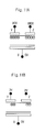
- FIGs. 11A and 11B are views illustrating wall charges not varied during first and second periods of FIG. 9;
- FIG. 12 is a view illustrating first and second periods of FIG. 9 depending on an AVL;
- FIG. 13 is a view illustrating a voltage waveform representing a driving method of a selective write and selective erase PDP according to a second embodiment of the present invention
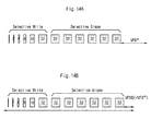
- FIG. 14A is a view illustrating a frame before a second embodiment of the present invention is applied.
- FIG. 14B is a view illustrating a frame after a second embodiment of the present invention is applied.
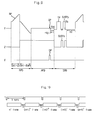
- FIG. 9 is a view illustrating a voltage waveform representing a driving method of a Plasma Display Panel (PDP) according to a first embodiment of the present invention.
- PDP Plasma Display Panel
- a sub-field (SF) included in one frame of the PDP is divided for an operation into a reset period (RPD), an address period (APD) and a sustain period (SPD).
- RPD reset period
- APD address period
- SPD sustain period
- a reset pulse (RP) is supplied to a scan electrode (Y) during the reset period (RPD).
- the reset pulse (RP) having a ramp wave format is in a way of increasing voltage during a set-up period and decreasing the voltage during a set-down period.
- a plurality of minute set-up discharges is generated to form the wall charge in an upper dielectric layer.
- unnecessary charged particles are partially removed due to a plurality of minute set-down charges such that the wall charge is decreased as much as a next address discharge is helped without an erroneous discharge.
- a positive-polar (+) direct-current voltage is supplied to a sustain electrode (Z) during the set-down period. Since the reset pulse (RP) is supplied gradually attenuating with respect to the positive-polar (+) direct-current voltage, the scan electrode (Y) has a relative negative polarity (-) with respect to the sustain electrode (Z), that is, polarity is inverted at the time of set-down thereby causing the wall charges generated at the time of set-up to be decreased.
- a scan pulse (SP) having a negative-polar (-) scan voltage (Vy) is supplied to the scan electrode (Y) and at the same time, a positive-polar (+) data pulse (DP) is supplied to the address electrode (X) thereby causing an address discharge.
- the wall charge formed due to the address discharge is maintained during a period during which other discharge cells are addressed.
- a first period (n1) of FIG. 9 is variably varied depending on the APL, as a period during which the scan voltage (Vsc) is continuously maintained after the scan pulse (SP) is applied.
- the second period (n2) is variably varied depending on the APL so as to coincide the light-emitting centers such that the flicker is removed thereby improving brightness.
- the first period (n1) is shortened, and if the APL is at a high level, the first period (n1) is lengthened. That is, since many sustain pulses are generated if the APL is at the low level, the first period (n1) is shortened, and since a few sustain pulses are generated if the APL is at the high level, the first period (n1) is lengthened.
- the address period (APD) of each of the sub-fields is varied by variably varying the first period (n1) depending on the APL as in FIG. 12. Accordingly, as in FIG. 10, an interval (T3) of a vertical frame blank (VFB) period between the frames is constantly maintained.
- the first period (n1) of FIG. 9 has a characteristic of not varying the wall charge as in FIG. 11A even though a period of 100 ⁇ s is maintained.
- a triggering pulse is supplied to the scan electrode (Y) such that a sustain discharge is initiated in the discharge cells where enough wall charges are formed during the address period (APD).
- sustain pulses SUSPz and SUSPy
- Vs sustain voltage
- a second period (n2) of FIG. 9 is variably varied depending on the APL, as a period till before a next sub-field begins after a last sustain pulse (SUSPz) is supplied during the sustain period (SPD).
- the flicker caused by the inconsistent light-emitting centers is removed. That is, the second period (n2) is variably varied depending on the APL so as to coincide the light-emitting centers such that the flicker is removed thereby improving the brightness.
- the second period (n2) is shortened as the period till before the next sub-field begins after the last sustain pulse (SUSPz) is supplied, and if the APL is at the high level, the second period (n2) is lengthened. That is, if the APL is at the low level, many sustain pulses are generated thereby causing much time to be relatively taken. Therefore, the second period (n2) is allowed to be short thereby secure the shortened time. To the contrary, if the APL is at the high level, the few sustain pulses are generated thereby causing little time to be relatively taken. Therefore, the second period (n2) can be lengthened.
- the sustain period is also varied to allow a length of each frame to be constant such that the interval of the vertical frame blank (VFB) period between the frames are constantly maintained thereby coinciding the light-emitting centers. That is, a variation of the address period (APD) of each of the sub-fields allows the periods during which the brightness of the n th frame and the (n+1) th frame are expressed as in FIG. 10 to be identically set. Accordingly, since the flicker is removed, the brightness is improved.
- the second period (n2) of FIG. 9 has the characteristic of not varying the wall charge as in FIG. 11B even though the period of 100 ⁇ s is maintained.
- any one of the first period (n1) or the second period (n2) can be variably varied to coincide the light-emitting centers.
- the first period (n1) or the second period (n2) can be all variably varied to coincide the light-emitting centers.
- FIG. 13 is a view illustrating a voltage waveform representing a driving method of a selective write and selective erase PDP according to a second embodiment of the present invention.
- one frame of the selective write and selective erase PDP is comprised of at least one selective write sub-field and at least one selective erase sub-field.
- the at least one selective write sub-field can be a selective write duration (SW6 and the like)
- the at least one selective erase sub-field can be a selective erase duration (SE1, SE2 and the like).
- the selective write sub-field is divided into a reset period (RPD), an address period (APD) and a sustain period (SPD), and the selective erase sub-field is divided into an address period (APD) and a sustain period (SPD).
- RPD reset period
- APD address period
- SPD sustain period
- SPD sustain period
- a set-down waveform ramp pulse (-RP) is sequentially supplied to scan electrode lines (Y) following a set-up waveform reset pulse (RP).
- the set-down waveform ramp pulse (-RP) drops to a negative-polar (-) scan reference voltage (-Vw). Further, a positive-polar (+) direct-current voltage is supplied to sustain electrode lines (Z).
- a negative-polar (-) selective write scan pulse (SWSP) and a positive-polar (+) selective write data pulse (SWDP) are supplied to each of the scan electrode lines (Y) and the address electrode lines (X) to be synchronized with each other.
- a first period (n11) of FIG. 13 is variably varied depending on an APL, as a period during which a scan voltage (Vsc) is continuously maintained after the scan pulse (SWSP) is applied during the address period (APD).
- the first period (n11) is variably varied depending on the APL to coincide the light-emitting centers such that the flicker is removed thereby improving brightness.
- the first period (n11) of FIG. 13 is variably varied depending on an APL, as the period during which the scan voltage (Vsc) is continuously maintained after the scan pulse (SWSP) is applied during the address period (APD), such that the address period (APD) of each sub-field is lengthened to reduce a long vertical frame blank (VFB*) period as in FIG. 14A to a short vertical frame blank (VFB$) period as in FIG. 14B. That is, the periods during which the brightness is expressed are identically set as in FIG.
- the first period (n11) is maintained during a different period depending on the APL as shown in FIG. 12.
- Sustain pulses are alternatively supplied to the scan electrode lines (Y) and the sustain electrode lines (Z) such that a sustain discharge is generated at a cell turned-on by the address discharge of the selective write sub-field during the sustain period (SPD) of the selective write sub-field.
- a second period (n12) of FIG. 13 is variably varied depending on the APL, as the period till before a next sub-field begins after the last sustain pulse (SUSPy) is supplied during the sustain period (SPD), such that the sustain period (SPD) of each sub-field is lengthened to reduce the long vertical frame blank (VFB*) period as in FIG. 14A to the short vertical frame blank (VFB$) period as in FIG. 14B.
- the second period (n12) is maintained during a different period depending on the APL as shown in FIG. 12.
- the reset period (RPD) of the selective erase sub-field is omitted.
- a negative-polar (-) selective erase scan pulse (SESP) and a positive-polar (+) selective erase data pulse (SEDP) are supplied to each of the scan electrode lines (Y) and the address electrode lines (X) to be synchronized with each other.
- the selective erase scan pulse (SESP) drops to a negative-polar (-) selective erase scan voltage (Ve) higher than the negative-polar (-) scan reference voltage (Vw).
- Vsc scan voltage
- SESP scan pulse
- APL address period
- VFB* long vertical frame blank
- VFB$ short vertical frame blank
- the third period (n13) is maintained during a different period depending on the APL as shown in FIG. 12.
- the sustain pulses (SUSPy and SUSPz) are alternatively supplied to the scan electrode lines (Y) and the sustain electrode lines (Z) such that the sustain discharge is generated at the cells not turned-off by the address discharge of the selective erase sub-field during the sustain period (SPD) of the selective erase sub-field.
- a fourth period (n14) of FIG. 13 is variably varied depending on the APL, as a period till before the next sub-field begins after the last sustain pulse (SUSPz) is supplied during the sustain period (SPD), such that the sustain period (SPD) of each sub-field is lengthened to reduce the long vertical frame blank (VFB*) period as in FIG. 14A to the short vertical frame blank (VFB$) period as in FIG. 14B.
- the periods during which the brightness is expressed are identically set as in FIG. 14B by varying the sustain period (SPD) of each sub-field.
- SPD sustain period
- the light-emitting centers coincide with one another such that the flicker can be removed thereby improving the brightness.
- the fourth period (n14) is maintained during the different period depending on the APL as shown in FIG. 12.
- the period between respective sub-fields or the period after the scan pulse during which the wall charge can be maintained without variation so as not to generate the erroneous discharge are controlled depending on the APL such that the flicker can be removed thereby improving the picture quality.
- the flicker caused by a way in which at least two frames are alternatively used every vertical synchronous signal to thereby increase the expression degree and the flicker caused by the 50Hz mode can be removed thereby improving the picture quality.
Landscapes
- Engineering & Computer Science (AREA)
- Physics & Mathematics (AREA)
- Power Engineering (AREA)
- Plasma & Fusion (AREA)
- Computer Hardware Design (AREA)
- General Physics & Mathematics (AREA)
- Theoretical Computer Science (AREA)
- Control Of Indicators Other Than Cathode Ray Tubes (AREA)
- Control Of Gas Discharge Display Tubes (AREA)
- Transforming Electric Information Into Light Information (AREA)
Applications Claiming Priority (2)
| Application Number | Priority Date | Filing Date | Title |
|---|---|---|---|
| KR2003015175 | 2003-03-11 | ||
| KR10-2003-0015175A KR100503603B1 (ko) | 2003-03-11 | 2003-03-11 | 플라즈마 디스플레이 패널의 구동방법 |
Publications (2)
| Publication Number | Publication Date |
|---|---|
| EP1457960A2 true EP1457960A2 (de) | 2004-09-15 |
| EP1457960A3 EP1457960A3 (de) | 2009-07-01 |
Family
ID=32768633
Family Applications (1)
| Application Number | Title | Priority Date | Filing Date |
|---|---|---|---|
| EP04075718A Withdrawn EP1457960A3 (de) | 2003-03-11 | 2004-03-11 | Ansteuerverfahren für einen Plasmabildschirm |
Country Status (5)
| Country | Link |
|---|---|
| US (2) | US7372435B2 (de) |
| EP (1) | EP1457960A3 (de) |
| JP (1) | JP2004272269A (de) |
| KR (1) | KR100503603B1 (de) |
| CN (1) | CN100446063C (de) |
Cited By (1)
| Publication number | Priority date | Publication date | Assignee | Title |
|---|---|---|---|---|
| EP1659557A2 (de) | 2004-11-22 | 2006-05-24 | Lg Electronics Inc. | Steuerung von Erhaltungsspannungen zur ein Plasmaanzeigetafel |
Families Citing this family (16)
| Publication number | Priority date | Publication date | Assignee | Title |
|---|---|---|---|---|
| KR100615253B1 (ko) * | 2004-09-24 | 2006-08-25 | 삼성에스디아이 주식회사 | 플라즈마 디스플레이 패널의 구동방법 |
| CN100385481C (zh) * | 2004-10-27 | 2008-04-30 | 南京Lg同创彩色显示系统有限责任公司 | 等离子显示器驱动方法及装置 |
| JP4801914B2 (ja) * | 2005-03-10 | 2011-10-26 | パナソニック株式会社 | プラズマディスプレイパネルの駆動方法 |
| JP5140933B2 (ja) * | 2005-03-31 | 2013-02-13 | パナソニック株式会社 | プラズマ・ディスプレイ・パネルの駆動方法 |
| JP4992195B2 (ja) * | 2005-04-13 | 2012-08-08 | パナソニック株式会社 | プラズマディスプレイパネルの駆動方法およびプラズマディスプレイ装置 |
| JP5017796B2 (ja) * | 2005-04-14 | 2012-09-05 | パナソニック株式会社 | プラズマディスプレイパネルの駆動方法およびプラズマディスプレイ装置 |
| JP4887722B2 (ja) * | 2005-10-14 | 2012-02-29 | パナソニック株式会社 | プラズマディスプレイパネルの駆動方法 |
| KR20080054433A (ko) * | 2006-08-31 | 2008-06-17 | 마츠시타 덴끼 산교 가부시키가이샤 | 플라즈마 디스플레이 장치 및 플라즈마 디스플레이 패널의구동 방법 |
| US9164037B2 (en) * | 2007-01-26 | 2015-10-20 | Palo Alto Research Center Incorporated | Method and system for evaluation of signals received from spatially modulated excitation and emission to accurately determine particle positions and distances |
| US8821799B2 (en) * | 2007-01-26 | 2014-09-02 | Palo Alto Research Center Incorporated | Method and system implementing spatially modulated excitation or emission for particle characterization with enhanced sensitivity |
| WO2012137791A1 (ja) | 2011-04-07 | 2012-10-11 | シャープ株式会社 | 表示装置、その駆動方法および電子機器 |
| TWI412016B (zh) * | 2011-05-11 | 2013-10-11 | Au Optronics Corp | 液晶顯示裝置及其驅動方法 |
| US9029800B2 (en) | 2011-08-09 | 2015-05-12 | Palo Alto Research Center Incorporated | Compact analyzer with spatial modulation and multiple intensity modulated excitation sources |
| US8723140B2 (en) | 2011-08-09 | 2014-05-13 | Palo Alto Research Center Incorporated | Particle analyzer with spatial modulation and long lifetime bioprobes |
| US9311872B2 (en) | 2011-08-12 | 2016-04-12 | Sharp Kabushiki Kaisha | Display device with timing controller |
| CN106097966B (zh) * | 2016-08-25 | 2019-01-29 | 深圳市华星光电技术有限公司 | 一种oled pwm像素驱动方法 |
Family Cites Families (13)
| Publication number | Priority date | Publication date | Assignee | Title |
|---|---|---|---|---|
| JP3499058B2 (ja) * | 1995-09-13 | 2004-02-23 | 富士通株式会社 | プラズマディスプレイの駆動方法及びプラズマディスプレイ装置 |
| US5818419A (en) * | 1995-10-31 | 1998-10-06 | Fujitsu Limited | Display device and method for driving the same |
| JPH10163671A (ja) | 1996-11-28 | 1998-06-19 | Mitsubishi Electric Corp | プラズマディスプレイ装置 |
| JP3620943B2 (ja) * | 1997-01-20 | 2005-02-16 | 富士通株式会社 | 表示方法及び表示装置 |
| TW412644B (en) | 1998-07-28 | 2000-11-21 | Sumitomo Chemical Co | Front panel for display |
| JP2994632B1 (ja) * | 1998-09-25 | 1999-12-27 | 松下電器産業株式会社 | 発光中心変動防止のためのpdp表示の駆動パルス制御装置 |
| EP1022714A3 (de) * | 1999-01-18 | 2001-05-09 | Pioneer Corporation | Verfahren zur Ansteuerung einer Plasmaanzeigetafel |
| JP2002544568A (ja) | 1999-05-14 | 2002-12-24 | スリーエム イノベイティブ プロパティズ カンパニー | アブレーション強化層 |
| US6555235B1 (en) | 2000-07-06 | 2003-04-29 | 3M Innovative Properties Co. | Touch screen system |
| JP2002040983A (ja) * | 2000-07-27 | 2002-02-08 | Sony Corp | 表示制御装置および表示制御方法 |
| US6587097B1 (en) | 2000-11-28 | 2003-07-01 | 3M Innovative Properties Co. | Display system |
| KR100404842B1 (ko) * | 2001-05-23 | 2003-11-07 | 엘지전자 주식회사 | 플라즈마 디스플레이 패널의 플리커 제거방법 및 장치 |
| JP5077860B2 (ja) * | 2001-05-31 | 2012-11-21 | 株式会社日立プラズマパテントライセンシング | Pdpの駆動方法および表示装置 |
-
2003
- 2003-03-11 KR KR10-2003-0015175A patent/KR100503603B1/ko not_active Expired - Fee Related
-
2004
- 2004-03-11 EP EP04075718A patent/EP1457960A3/de not_active Withdrawn
- 2004-03-11 JP JP2004068980A patent/JP2004272269A/ja not_active Withdrawn
- 2004-03-11 CN CNB2004100046980A patent/CN100446063C/zh not_active Expired - Fee Related
- 2004-03-11 US US10/797,578 patent/US7372435B2/en not_active Expired - Fee Related
-
2007
- 2007-09-13 US US11/854,726 patent/US20080174524A1/en not_active Abandoned
Cited By (4)
| Publication number | Priority date | Publication date | Assignee | Title |
|---|---|---|---|---|
| EP1659557A2 (de) | 2004-11-22 | 2006-05-24 | Lg Electronics Inc. | Steuerung von Erhaltungsspannungen zur ein Plasmaanzeigetafel |
| EP1659557A3 (de) * | 2004-11-22 | 2006-07-05 | Lg Electronics Inc. | Steuerung von Erhaltungsspannungen zur ein Plasmaanzeigetafel |
| CN100437693C (zh) * | 2004-11-22 | 2008-11-26 | Lg电子株式会社 | 等离子显示设备 |
| US7911421B2 (en) | 2004-11-22 | 2011-03-22 | Lg Electronics Inc. | Driving device and method for plasma display panel |
Also Published As
| Publication number | Publication date |
|---|---|
| JP2004272269A (ja) | 2004-09-30 |
| KR20040080271A (ko) | 2004-09-18 |
| US7372435B2 (en) | 2008-05-13 |
| KR100503603B1 (ko) | 2005-07-26 |
| US20080174524A1 (en) | 2008-07-24 |
| US20040233135A1 (en) | 2004-11-25 |
| EP1457960A3 (de) | 2009-07-01 |
| CN1530912A (zh) | 2004-09-22 |
| CN100446063C (zh) | 2008-12-24 |
Similar Documents
| Publication | Publication Date | Title |
|---|---|---|
| US20080174524A1 (en) | Driving method of plasma display panel | |
| KR100281019B1 (ko) | 플라즈마 디스플레이 패널의 구동 방법 | |
| JP3429438B2 (ja) | Ac型pdpの駆動方法 | |
| JP4322101B2 (ja) | プラズマディスプレイ装置 | |
| KR100607253B1 (ko) | 플라즈마 디스플레이 패널의 구동장치 | |
| KR100542772B1 (ko) | 플라즈마 디스플레이 패널 구동방법 및 장치 | |
| KR100647776B1 (ko) | 플라즈마 디스플레이 패널의 구동방법 | |
| KR20040092297A (ko) | 플라즈마 디스플레이 패널의 구동방법 및 장치 | |
| US20060145957A1 (en) | Plasma display device and method of driving the same | |
| KR100580556B1 (ko) | 플라즈마 디스플레이 패널의 구동방법 | |
| KR100487001B1 (ko) | 플라즈마 디스플레이 패널의 구동방법 | |
| WO2010146827A1 (ja) | プラズマディスプレイパネルの駆動方法およびプラズマディスプレイ装置 | |
| KR100492184B1 (ko) | 플라즈마 디스플레이 패널의 구동방법 | |
| KR100280888B1 (ko) | 플라즈마 디스플레이 패널과 그 구동 장치 및 방법 | |
| WO2009125910A1 (en) | Plasma display device | |
| KR100547977B1 (ko) | 플라즈마 디스플레이 패널의 구동방법 | |
| JP5107958B2 (ja) | プラズマディスプレイ装置 | |
| KR100489278B1 (ko) | 플라즈마 디스플레이 패널의 구동방법 | |
| KR100837660B1 (ko) | 플라즈마 디스플레이 장치 | |
| KR100675323B1 (ko) | 플라즈마 디스플레이 패널의 구동방법 | |
| KR100493621B1 (ko) | 플라즈마 디스플레이 패널의 구동방법 | |
| US8319705B2 (en) | Plasma display device and driving method using all cell reset and on cell reset operations | |
| KR20060086775A (ko) | 플라즈마 디스플레이 패널의 구동방법 | |
| KR20020094316A (ko) | 플라즈마 디스플레이 패널의 소거방전 구동방법 | |
| KR20030061077A (ko) | 플라즈마 디스플레이 패널의 구동 방법 |
Legal Events
| Date | Code | Title | Description |
|---|---|---|---|
| PUAI | Public reference made under article 153(3) epc to a published international application that has entered the european phase |
Free format text: ORIGINAL CODE: 0009012 |
|
| AK | Designated contracting states |
Kind code of ref document: A2 Designated state(s): AT BE BG CH CY CZ DE DK EE ES FI FR GB GR HU IE IT LI LU MC NL PL PT RO SE SI SK TR |
|
| AX | Request for extension of the european patent |
Extension state: AL HR LT LV MK |
|
| RIN1 | Information on inventor provided before grant (corrected) |
Inventor name: KYU SEON, LEE Inventor name: JEONG PIL, CHOI Inventor name: DAI HYUN, KIM |
|
| RIC1 | Information provided on ipc code assigned before grant |
Ipc: G09G 3/288 20060101ALI20090225BHEP Ipc: G09G 3/28 20060101AFI20040511BHEP |
|
| PUAL | Search report despatched |
Free format text: ORIGINAL CODE: 0009013 |
|
| AK | Designated contracting states |
Kind code of ref document: A3 Designated state(s): AT BE BG CH CY CZ DE DK EE ES FI FR GB GR HU IE IT LI LU MC NL PL PT RO SE SI SK TR |
|
| AX | Request for extension of the european patent |
Extension state: AL LT LV MK |
|
| STAA | Information on the status of an ep patent application or granted ep patent |
Free format text: STATUS: THE APPLICATION IS DEEMED TO BE WITHDRAWN |
|
| AKX | Designation fees paid | ||
| 18D | Application deemed to be withdrawn |
Effective date: 20091001 |
|
| REG | Reference to a national code |
Ref country code: DE Ref legal event code: 8566 |