EP1457515A1 - Resin composition prepreg laminated sheet and semiconductor package - Google Patents
Resin composition prepreg laminated sheet and semiconductor package Download PDFInfo
- Publication number
- EP1457515A1 EP1457515A1 EP02772828A EP02772828A EP1457515A1 EP 1457515 A1 EP1457515 A1 EP 1457515A1 EP 02772828 A EP02772828 A EP 02772828A EP 02772828 A EP02772828 A EP 02772828A EP 1457515 A1 EP1457515 A1 EP 1457515A1
- Authority
- EP
- European Patent Office
- Prior art keywords
- prepreg
- resin
- resin composition
- thermosetting
- filler
- Prior art date
- Legal status (The legal status is an assumption and is not a legal conclusion. Google has not performed a legal analysis and makes no representation as to the accuracy of the status listed.)
- Withdrawn
Links
Images


Classifications
-
- C—CHEMISTRY; METALLURGY
- C08—ORGANIC MACROMOLECULAR COMPOUNDS; THEIR PREPARATION OR CHEMICAL WORKING-UP; COMPOSITIONS BASED THEREON
- C08J—WORKING-UP; GENERAL PROCESSES OF COMPOUNDING; AFTER-TREATMENT NOT COVERED BY SUBCLASSES C08B, C08C, C08F, C08G or C08H
- C08J5/00—Manufacture of articles or shaped materials containing macromolecular substances
- C08J5/24—Impregnating materials with prepolymers which can be polymerised in situ, e.g. manufacture of prepregs
- C08J5/241—Impregnating materials with prepolymers which can be polymerised in situ, e.g. manufacture of prepregs using inorganic fibres
-
- H—ELECTRICITY
- H05—ELECTRIC TECHNIQUES NOT OTHERWISE PROVIDED FOR
- H05K—PRINTED CIRCUITS; CASINGS OR CONSTRUCTIONAL DETAILS OF ELECTRIC APPARATUS; MANUFACTURE OF ASSEMBLAGES OF ELECTRICAL COMPONENTS
- H05K1/00—Printed circuits
- H05K1/02—Details
- H05K1/03—Use of materials for the substrate
- H05K1/0313—Organic insulating material
- H05K1/0353—Organic insulating material consisting of two or more materials, e.g. two or more polymers, polymer + filler, + reinforcement
- H05K1/0373—Organic insulating material consisting of two or more materials, e.g. two or more polymers, polymer + filler, + reinforcement containing additives, e.g. fillers
-
- C—CHEMISTRY; METALLURGY
- C08—ORGANIC MACROMOLECULAR COMPOUNDS; THEIR PREPARATION OR CHEMICAL WORKING-UP; COMPOSITIONS BASED THEREON
- C08J—WORKING-UP; GENERAL PROCESSES OF COMPOUNDING; AFTER-TREATMENT NOT COVERED BY SUBCLASSES C08B, C08C, C08F, C08G or C08H
- C08J5/00—Manufacture of articles or shaped materials containing macromolecular substances
- C08J5/24—Impregnating materials with prepolymers which can be polymerised in situ, e.g. manufacture of prepregs
-
- C—CHEMISTRY; METALLURGY
- C08—ORGANIC MACROMOLECULAR COMPOUNDS; THEIR PREPARATION OR CHEMICAL WORKING-UP; COMPOSITIONS BASED THEREON
- C08J—WORKING-UP; GENERAL PROCESSES OF COMPOUNDING; AFTER-TREATMENT NOT COVERED BY SUBCLASSES C08B, C08C, C08F, C08G or C08H
- C08J5/00—Manufacture of articles or shaped materials containing macromolecular substances
- C08J5/24—Impregnating materials with prepolymers which can be polymerised in situ, e.g. manufacture of prepregs
- C08J5/241—Impregnating materials with prepolymers which can be polymerised in situ, e.g. manufacture of prepregs using inorganic fibres
- C08J5/244—Impregnating materials with prepolymers which can be polymerised in situ, e.g. manufacture of prepregs using inorganic fibres using glass fibres
-
- C—CHEMISTRY; METALLURGY
- C08—ORGANIC MACROMOLECULAR COMPOUNDS; THEIR PREPARATION OR CHEMICAL WORKING-UP; COMPOSITIONS BASED THEREON
- C08J—WORKING-UP; GENERAL PROCESSES OF COMPOUNDING; AFTER-TREATMENT NOT COVERED BY SUBCLASSES C08B, C08C, C08F, C08G or C08H
- C08J5/00—Manufacture of articles or shaped materials containing macromolecular substances
- C08J5/24—Impregnating materials with prepolymers which can be polymerised in situ, e.g. manufacture of prepregs
- C08J5/249—Impregnating materials with prepolymers which can be polymerised in situ, e.g. manufacture of prepregs characterised by the additives used in the prepolymer mixture
-
- H—ELECTRICITY
- H05—ELECTRIC TECHNIQUES NOT OTHERWISE PROVIDED FOR
- H05K—PRINTED CIRCUITS; CASINGS OR CONSTRUCTIONAL DETAILS OF ELECTRIC APPARATUS; MANUFACTURE OF ASSEMBLAGES OF ELECTRICAL COMPONENTS
- H05K1/00—Printed circuits
- H05K1/02—Details
- H05K1/03—Use of materials for the substrate
- H05K1/0313—Organic insulating material
- H05K1/0353—Organic insulating material consisting of two or more materials, e.g. two or more polymers, polymer + filler, + reinforcement
- H05K1/0366—Organic insulating material consisting of two or more materials, e.g. two or more polymers, polymer + filler, + reinforcement reinforced, e.g. by fibres, fabrics
-
- H—ELECTRICITY
- H05—ELECTRIC TECHNIQUES NOT OTHERWISE PROVIDED FOR
- H05K—PRINTED CIRCUITS; CASINGS OR CONSTRUCTIONAL DETAILS OF ELECTRIC APPARATUS; MANUFACTURE OF ASSEMBLAGES OF ELECTRICAL COMPONENTS
- H05K2201/00—Indexing scheme relating to printed circuits covered by H05K1/00
- H05K2201/02—Fillers; Particles; Fibers; Reinforcement materials
- H05K2201/0203—Fillers and particles
- H05K2201/0206—Materials
- H05K2201/0209—Inorganic, non-metallic particles
-
- Y—GENERAL TAGGING OF NEW TECHNOLOGICAL DEVELOPMENTS; GENERAL TAGGING OF CROSS-SECTIONAL TECHNOLOGIES SPANNING OVER SEVERAL SECTIONS OF THE IPC; TECHNICAL SUBJECTS COVERED BY FORMER USPC CROSS-REFERENCE ART COLLECTIONS [XRACs] AND DIGESTS
- Y10—TECHNICAL SUBJECTS COVERED BY FORMER USPC
- Y10T—TECHNICAL SUBJECTS COVERED BY FORMER US CLASSIFICATION
- Y10T428/00—Stock material or miscellaneous articles
- Y10T428/24—Structurally defined web or sheet [e.g., overall dimension, etc.]
- Y10T428/24802—Discontinuous or differential coating, impregnation or bond [e.g., artwork, printing, retouched photograph, etc.]
- Y10T428/24917—Discontinuous or differential coating, impregnation or bond [e.g., artwork, printing, retouched photograph, etc.] including metal layer
-
- Y—GENERAL TAGGING OF NEW TECHNOLOGICAL DEVELOPMENTS; GENERAL TAGGING OF CROSS-SECTIONAL TECHNOLOGIES SPANNING OVER SEVERAL SECTIONS OF THE IPC; TECHNICAL SUBJECTS COVERED BY FORMER USPC CROSS-REFERENCE ART COLLECTIONS [XRACs] AND DIGESTS
- Y10—TECHNICAL SUBJECTS COVERED BY FORMER USPC
- Y10T—TECHNICAL SUBJECTS COVERED BY FORMER US CLASSIFICATION
- Y10T428/00—Stock material or miscellaneous articles
- Y10T428/249921—Web or sheet containing structurally defined element or component
- Y10T428/249924—Noninterengaged fiber-containing paper-free web or sheet which is not of specified porosity
-
- Y—GENERAL TAGGING OF NEW TECHNOLOGICAL DEVELOPMENTS; GENERAL TAGGING OF CROSS-SECTIONAL TECHNOLOGIES SPANNING OVER SEVERAL SECTIONS OF THE IPC; TECHNICAL SUBJECTS COVERED BY FORMER USPC CROSS-REFERENCE ART COLLECTIONS [XRACs] AND DIGESTS
- Y10—TECHNICAL SUBJECTS COVERED BY FORMER USPC
- Y10T—TECHNICAL SUBJECTS COVERED BY FORMER US CLASSIFICATION
- Y10T428/00—Stock material or miscellaneous articles
- Y10T428/25—Web or sheet containing structurally defined element or component and including a second component containing structurally defined particles
- Y10T428/259—Silicic material
Definitions
- This invention relates to a resin composition, a prepreg, a laminate, and a semiconductor package.
- a prepreg used for a printed wiring board is formed by impregnating a base material such as glass cloth or the like with a varnish made of a thermosetting resin such as epoxy resin, cyanate resin or the like and then drying it by heating with being reacted.
- a base material such as glass cloth or the like
- a varnish made of a thermosetting resin such as epoxy resin, cyanate resin or the like
- thermosetting resin constituting the prepreg is cured to a semi-cured state in the above-mentioned heating and reacting process, to thereby suppress development of tack on the surface of the prepreg and control resin flow when the prepregs are heated and pressed during laminating.
- the present invention is directed to a resin composition which is used to form a sheet-shaped prepreg by being impregnated into a base material, wherein the resin composition comprises a first thermosetting resin having a weight average molecular weight, a second thermosetting resin having a lower weight average molecular weight than that of the first thermosetting resin, a curing agent, and a filler.
- the resin composition further comprises a resin of which moisture absorption is lower than that of both of the first thermosetting resin and the second thermosetting resin.
- first and second thermosetting resins include epoxy resin or cyanate resin.
- the weight average molecular weight of the first thermosetting resin is equal to or more than 2,000.
- the weight average molecular weight of the second thermosetting resin is equal to or less than 1,500.
- At least one of the first and second thermosetting resins contains cyanate resin.
- the cyanate resin is preferably a novolak type cyanate resin.
- thermosetting resin and/or the curing agent is in a liquid state at room temperature.
- the filler is an inorganic filler in powder form.
- the filler is preferably silica.
- the filler is in powder form and that the average particle size of the filler is equal to or less than 2 ⁇ m.
- the content of the filler is 40 to 80 wt% of the total weight of the resin composition.
- Another aspect of the present invention is directed to a prepreg formed by impregnating a base material with the resin composition described above.
- the reaction rate of the resin composition in the prepreg is preferably equal to or less than 30 %.
- the base material is a spread-out glass fiber base material.
- the base material is a nonwoven fabric made of organic fibers.
- a metallic foil is laminated on at least one of the surfaces of the prepreg.
- Yet another aspect of the present invention is directed to a laminate formed by laminating a metallic foil on at least one of the surfaces of the prepreg described above and then molding them by heating under pressure.
- Still another aspect of the present invention is directed to a semiconductor package manufactured by mounting at least one IC chip on the prepreg described above.
- the resin composition of the present invention is used for forming a sheet-shaped prepreg by being impregnated into a base material.
- the resin composition of the present invention includes a first thermosetting resin, a second thermosetting resin having a lower weight average molecular weight than that of the first thermosetting resin, a curing agent, and a filler.
- the prepreg of the present invention is formed by impregnating a base material with the resin composition described above.
- the laminate of the present invention is formed by laminating a metallic foil on at least one of the surfaces of the prepreg described above and then molding them by heating under pressure.
- the semiconductor package of the present invention is manufactured by mounting at least one IC chip on the prepreg with the metallic foil.
- the resin composition of the present invention includes a first thermosetting resin and a second thermosetting resin having a lower weight average molecular weight than that of the first thermosetting resin. This makes it possible to impart flexibility to a prepreg. In addition, it is also possible to prevent cracking from occurring in a prepreg. As a result, a prepreg formed using the resin composition of the present invention can have an excellent withstanding property for processing operations during circuit formation processing.
- the withstanding property for processing operations means properties of prepregs by which cracking due to a pressure between a feed roll and a guide roll will not occur during feeding of materials (prepregs), and cracking due to the spray pressure of an etchant during etching in the circuit formation processing will not occur, for example. Further, when a prepreg has flexibility, it is possible to continuously take up the prepreg.
- the weight average molecular weight of the first thermosetting resin (especially, cyanate resin) is not limited to any specific value, but is preferably equal to or more than 2,000, and more preferably 2,200 to 10,000. If the weight average molecular weight of the first thermosetting resin exceeds the above upper limit value, the viscosity of a varnish made of the resin composition is increased, thus resulting in the case that the impregnability of the resin into a base material is lowered. On the other hand, if the weight average molecular weight of the first thermosetting resin is less than the above lower limit value, there is a case that an excessive flow of the resin composition occurs during laminating of prepregs.
- the weight average molecular weight of the first thermosetting resin is within the above range, it is possible to prevent development of tack on the surface of a prepreg even in the case where the resin composition in the prepreg is in an uncured state. Preventing such development of tack makes it possible to improve workability in feeding a prepreg.
- the weight average molecular weight of the second thermosetting resin (especially, cyanate resin) is not limited to any specific value, but is preferably equal to or less than 1,500, and more preferably 200 to 1,300. If the weight average molecular weight of the second thermosetting resin exceeds the above upper limit value, there is a case that the effect of suppressing generation of dust from a prepreg is lowered. On the other hand, if the weight average molecular weight of the second thermosetting resin is less than the above lower limit value, there is a case that an excessive flow of the resin composition occurs during the laminating of prepregs.
- a prepreg When the weight average molecular weight of the second thermosetting resin is within the above range, a prepreg can have an improved flexibility. In addition, it is possible to suppress generation of dust from a prepreg. Further, it is also possible to improve dispersibility of a filler (which will be described later) in the resin composition.
- thermosetting resins can be measured by, for example, gel permeation chromatography using polystyrene as a standard.
- the first thermosetting resin (especially, cyanate resin) is not limited to a specific one, but one which is in a solid state at room temperature is preferably used. This makes it possible to prevent development of tack on the surface of a prepreg even in the case where the resin composition in the prepreg is in an uncured state.
- the second thermosetting resin (especially, cyanate resin) is not limited to a specific one, but one which is in a liquid state at room temperature is preferably used. This makes it possible to improve the flexibility of a prepreg. In addition, it is also possible to suppress generation of dust from a prepreg.
- liquid state is a state that exhibits flowability or fluidity at room temperature.
- the viscosity of the second thermosetting resin described above is not limited to any specific value, but is preferably equal to or less than 500 Pa ⁇ s, and more preferably 300 to 1 Pa ⁇ s.
- the viscosity is measured using an E type viscometer under the condition that a shear rate is each of 0.5, 1.0, 2.5, and 5.0 rpm at a temperature of 25°C. A value obtained at the lowest rpm in the shear rates at which measurement can be made is practically used as the viscosity mentioned above.
- thermosetting resins examples include epoxy resin, phenolic resin, urea resin, melamine resin, silicon resin, polyester resin, cyanate resin, and the like. Among these resins, epoxy resin and/or cyanate resin are preferably used.
- epoxy resin examples include: phenol-based epoxy resin such as bisphenol type epoxy resin, phenol novolak type epoxy resin, alkylphenol novolak type epoxy resin, biphenol type epoxy resin, naphthol type epoxy resin, resorcinol type epoxy resin, and the like; and modified epoxy resin having an aliphatic structure, a cycloaliphatic structure, an unsaturated aliphatic structure, or the like as a base structure.
- phenol-based epoxy resin such as bisphenol type epoxy resin, phenol novolak type epoxy resin, alkylphenol novolak type epoxy resin, biphenol type epoxy resin, naphthol type epoxy resin, resorcinol type epoxy resin, and the like
- modified epoxy resin having an aliphatic structure, a cycloaliphatic structure, an unsaturated aliphatic structure, or the like as a base structure.
- the cyanate resin described above can be obtained, for example, by reacting a halogenated cyanogen compound and phenols.
- the cyanate resin include novolak type cyanate resin, bisphenol type cyanate resin, and the like.
- at least one of the first thermosetting resin and the second thermosetting resin contains cyanate resin (especially, novolak type cyanate resin).
- the content of the novolak type cyanate resin is 10 wt% or more of the total weight of the resin composition). This makes it possible to improve the heat resistance (glass transition temperature and thermal decomposition temperature) of a prepreg.
- a prepreg especially, the coefficient of thermal expansion of a prepreg in the thickness direction.
- strain induced by stress can be reduced in a multi-layer printed wiring board.
- a multi-layer printed circuit board it is also possible for a multi-layer printed circuit board to have significantly improved connection reliability of micro interlayer connections.
- the first and second thermosetting resins may have different molecular structures from each other, but they preferably have the same molecular structure. By using thermosetting resins having the same molecular structure, it is possible to improve compatibility between cyanate resins having different molecular weights from each other.
- thermosetting resins As for the first and second thermosetting resins, a novolak type cyanate resin represented by the formula (I) is preferably used, for example. (wherein, n is an arbitrary integer)
- the weight average molecular weight of the resin is not limited to any specific value, but is preferably 2,000 to 10,000, and more preferably 2,200 to 3,500.
- the weight average molecular weight of the resin is within the above range, it is possible to effectively prevent development of tack on the surface of a prepreg even in the case where the resin in the prepreg is in an uncured state.
- the weight average molecular weight of the resin is not limited to any specific value, but is preferably 300 to 2,000, and more preferably 500 to 1,500.
- the weight average molecular weight of the resin is within the above range, it is possible to further improve the flexibility of a prepreg. In addition, it is also possible to suppress generation of dust from a prepreg. Further, it is also possible to improve dispersibilty of a filler (which will be described later) in the resin composition.
- the content of the first thermosetting resin is not limited to any specific value, but is preferably 5 to 23 wt% of the total weight of the resin composition, and more preferably 6 to 18 wt%.
- the content of the first thermosetting resin is within the above range, it is possible to prevent development of tack on the surface of a prepreg even in the case where the resin in the prepreg is in an uncured state.
- the content of the second thermosetting resin is not limited to any specific value, but is preferably 2 to 15 wt% of the total weight of the resin composition, and more preferably 4 to 10 wt%.
- the content of the second thermosetting resin is within the above range, it is possible to suppress generation of dust from a prepreg as well as to further improve the flexibility of a prepreg.
- the resin composition further includes a resin of which moisture absorption is lower than that of both of the first and second thermosetting resins.
- the resin composition includes such a resin, the moisture resistance (especially, solder heat resistance after moisture absorption) of a prepreg can be improved.
- a resin having low moisture absorption a resin of which oxygen atom content (especially, oxygen atom in hydroxyl group) is low is preferably used. (Especially, a resin of which oxygen atom content is equal to or less than 5 wt% is preferably used.) Also, a resin which has high crystallinity and high packing degree, and is comprised of molecules containing only C, H, Cl, and F is preferably used.
- the resin does not contain halogens from the viewpoint of recent trend of environmental protection.
- a resin having a resin structure containing at least one selected from the group including a naphthalene structure, a biphenyl structure, and a cyclopentadiene structure can be mentioned.
- naphthol novolak type epoxy resin and the like can be mentioned.
- epoxy resin especially, aryl-alkyl type epoxy resin
- aryl-alkyl type epoxy resin is especially preferable. By using biphenyl type epoxy resin, it is possible for a prepreg to have excellent heat resistance as well as improved moisture resistance.
- thermosetting resin having low moisture absorption is used as a first thermosetting resin and a second thermosetting resin instead of a cyanate resin, there is no necessity to add another resin having low moisture absorption described above.
- the content of the resin having low moisture absorption is preferably equal to or less than 20 wt% of the total weight of the resin composition, and more preferably 10 to 18 wt%.
- the resin composition of the present invention may further include a curing agent. This makes it possible to control the cross-linking density of the thermosetting resins.
- examples of the curing agent include: organometallic salt such as zinc naphthenate, cobalt naphthenate, tin octylate, or cobalt octylate; tertiary amines such as triethylamine, tributylamine, or diazabicyclo [2, 2, 2] octane; imidazoles such as 2-phenyl-4-methylimidazole, 2-ethyl-4-methylimidazole, 2-phenyl-4,5-dihydroxymethylimidazole, or 2-phenyl-4-methyl-5-hydroxymethylimidazole; phenolic compound such as phenol, bisphenol A, or nonyl phenol; phenolic resin; organic acid; and the like.
- phenolic resin especially, phenol novolak resin
- phenolic resin is preferably used.
- examples of the curing agent include: tertiary amines such as triethylamine, tributylamine, or diazabicyclo [2, 2, 2] octane; imidazoles such as 2-phenyl-4-methylimidazole, 2-ethyl-4-methylimidazole, 2-phenyl-4,5-dihydroxymethylimidazole, or 2-phenyl-4-methyl-5-hydroxymethylimidazole; phenolic compound such as phenol, bisphenol A, or nonyl phenol; phenolic resin; organic acid; and the like. These curing agents may be used alone or in combination.
- tertiary amines such as triethylamine, tributylamine, or diazabicyclo [2, 2, 2] octane
- imidazoles such as 2-phenyl-4-methylimidazole, 2-ethyl-4-methylimidazole, 2-phenyl-4,5-dihydroxymethylimidazole, or 2-pheny
- the content of the curing agent is not limited to any specific value, but is preferably 0.01 to 5 wt% of the total weight of the resin composition, and more preferably 0.05 to 3 wt%. When the content of the curing agent is within the above range, it is possible for a prepreg to have excellent moisture resistance and heat resistance.
- the functional group equivalent of the curing agent is preferably 50 to 100% of that of the resin having low moisture absorption.
- the content of the curing agent and the resin having low moisture absorption is preferably equal to or less than 15 wt% of the total weight of the resin composition.
- the curing agent which also acts on the resin having low moisture absorption as a curing agent therefor is not limited to a specific one, and curing agents which are in a liquid state at room temperature may be used as such a curing agent.
- the resin composition of the present invention further includes a filler. This makes it possible to control resin flow during laminating (molding) of uncured state prepregs. By controlling resin flow, it is possible to improve moldability during laminating (molding) of prepregs for forming a laminate.
- the filler is not limited to a specific one, but one which is in powder form is preferable, and an inorganic filler in powder form is more preferable. By using such a filler, control of the flowability of the resin composition can be made more suitably. In addition, it is also possible for a prepreg to have lower thermal expansibility.
- the filler examples include: silicate such as talc, clay, mica, or glass; oxide such as alumina or silica; carbonate such as calcium carbonate or magnesium carbonate; hydroxide such as aluminum hydroxide or magnesium hydroxide; and the like. Among them, oxide such as silica or the like is preferably used.
- silica fused silica is preferably used.
- shape of silica particle is either sphere or flake
- silica comprised of spherical particles is preferably used from the viewpoint of a reduction in the melt viscosity of the resin composition so that the impregnability of the resins into a glass base material is ensured.
- the average particle size of the filler is not limited to any specific value, but is preferably equal to or less than 2 ⁇ m, and more preferably 0.2 to 1 ⁇ m. By using the filler having the average particle size within the above range, it is possible to impart thixotropy to the resin composition. In addition, it is possible to satisfactorily control the flowability of the resins.
- the content of the filler is not limited to any specific value, but is preferably 40 to 80 wt% of the total weight of the resin composition, and more preferably 50 to 70 wt%. By setting the content of the filler to the above range, it is possible to impart thixotropy to the resin composition. When the resin composition has thixotropy, it is possible to control resin flow during press molding of prepregs.
- a prepreg 1 of the present invention is a sheet-shaped prepreg formed by impregnating a base material with the resin composition described above. In this way, it is possible to obtain a prepreg having excellent flexibility. Further, it is also possible to obtain a prepreg in which cracking is difficult to occur.
- the prepreg 1 is constituted from a sheet-shaped base material 11 and a resin composition 12.
- the base material examples include: glass fiber base material such as glass woven fabric, glass nonwoven fabric, or glass paper; woven fabric and nonwoven fabric which are made of organic fibers such as paper fibers (pulp), aramid fibers, polyester fibers, or fluoropolymer fibers; woven fabric, nonwoven fabric, and mat which are made of metallic fibers, carbon fibers, or mineral fibers; and the like. These base materials may be used alone or in combination. Among them, nonwoven fabric made of organic fibers is preferably used. By using such a base material, it is possible to improve the processability in forming via holes in the prepreg with laser.
- glass fiber base material such as glass woven fabric, glass nonwoven fabric, or glass paper
- woven fabric and nonwoven fabric which are made of organic fibers such as paper fibers (pulp), aramid fibers, polyester fibers, or fluoropolymer fibers
- woven fabric, nonwoven fabric, and mat which are made of metallic fibers, carbon fibers, or mineral fibers; and the like
- a spread-out glass fiber base material refers to one in which warp yarns and weft yarns are both arranged without substantially any gap.
- Examples of a method for impregnating the resin composition into the base material include: immersion of the base material into a resin varnish; coating a resin varnish on the base material using various coaters; spraying a resin varnish to the base material using a spray; or the like.
- immersion of the base material into a resin varnish is preferably used.
- a commonly used impregnation and coating machine can be used for immersion of the base material into a resin varnish.
- a solvent for use in preparing a resin varnish it is desirable that a solvent which has good solubility to the resin composition is preferably used. However, a poor solvent may be added to the solvent as long as the solvent does not receive any adverse effect. Examples of the solvent which has good solubility to the resin composition include methyl ethyl ketone, cyclohexanone, and the like.
- the solid content of the resin varnish is not limited to any specific value, but is preferably 40 to 80 wt%, and more preferably 50 to 70 wt%. By setting the content of the resin varnish to the above range, it is possible to further improve the impregnability of the resin varnish into the base material.
- the prepreg of the present invention can be used with the resin in the prepreg being cured by heating as is the same manner as the conventional prepreg, the prepreg of the present invention may be used with the resin being in an uncured state. Also, the prepreg of the present invention may be used with the resin being cured to a semi-cured state which is a state between a cured state and an uncured state. Specifically, it is possible to laminate a metallic foil on a prepreg, even in the case where the prepreg is being in an uncured state, and it is also possible to form a circuit on such a prepreg with the metallic foil.
- the reaction rate of the resin composition in the prepreg is not limited to any specific value, but is preferably equal to or less than 30 %, and more preferably 0.1 to 20 %. By setting the reaction rate to the above range, it is possible to prevent dust from being generated as well as to produce the above-described effect.
- a conventional prepreg has problems in that the reaction rate of a resin composition in the prepreg is about 60 to 80 % so that the prepreg lacks in flexibility, and that dust is generated.
- the prepreg of the present invention can be used with the resin in the prepreg being in an uncured state or a state in which reaction rate is low, because the prepreg has flexibility.
- the reaction rate described above can be determined by means of differential scanning calorimetry (DSC). Specifically, the reaction rate can be determined by comparing areas at the exothermic peaks during reaction in DSC between an unreacted resin composition and the resin composition in the prepreg of the present invention, and practically it is determined based on the following formula (I). It is to be noted that measurement by means of DSC is made at a temperature elevation rate of 10°C/min and in an atmosphere of nitrogen.
- Reaction rate (%) (1 - area at exothermic peak during reaction of resin composition in prepreg / area at exothermic peak during reaction of unreacted resin composition) ⁇ 100 (I)
- a sample for use in determining the area at the exothermic peak of the unreacted resin composition is prepared by impregnating a base material with a resin varnish, made of the resin composition of the present invention and a solvent, to obtain a prepreg, air-drying the prepreg at 40°C for 10 minutes, and then removing the solvent from the prepreg in a vacuum of 1 kPa, at 40°C for 1 hour.
- a prepreg (a prepreg with a metallic foil) obtained by laminating a metallic foil on at least one of the surfaces of the prepreg described above.
- a prepreg with a metallic foil 2 is constituted from a prepreg which is formed from a sheet-shaped base material 21 and a resin composition 22, and a metallic foil 23, wherein the metallic foil 23 is laminated on one of the surfaces of the prepreg.
- the resin composition may be in an uncured state or a semi-cured state.
- the reaction rate of the resin composition in the prepreg with the metallic foil is not limited to any specific value, but is preferably equal to or less than 30%, and more preferably 0.1 to 20 %.
- the reaction rate of the resin composition in the prepreg with the metallic foil lies in the above range, it is possible for the prepreg to be subjected to circuit formation processing. In addition, it is possible to improve the processability in forming via holes in the prepreg with laser.
- Examples of a metallic material used for forming a metallic foil include copper or copper based alloy; aluminum or aluminum based alloy; and the like.
- the thickness of the metallic foil is preferably 3 to 70 ⁇ m, and more preferably 12 to 35 ⁇ m.
- the metallic foils may be respectively laminated on both surfaces of the prepreg.
- the laminate of the present invention is formed by laminating a metallic foil on at least one of the surfaces of the prepreg described above and then molding them by heating under pressure.
- a metallic foil or film is laminated on one or both of the surfaces of the prepreg.
- a metallic foil or film is laminated on one or both of the outermost surfaces of the laminated prepregs.
- the laminate of the present invention is formed by heating the prepreg with the laminated metallic foil under pressure.
- the heating temperature is not limited to any specific value, but is preferably 120 to 220°C, and more preferably 150 to 200°C.
- the pressure is not also limited to any specific value, but is preferably 2 to 5 MPa, and more preferably 2.5 to 4 MPa.
- the semiconductor package of the present invention is formed by mounting at least one IC chip on the prepreg with the metallic foil described above.
- a semiconductor package 3 of the present invention includes a prepreg with a metallic foil 31, on which a circuit is formed, a solder resist layer 32, and an IC chip 33.
- the prepreg with a circuit 31 can be obtained by, for example, subjecting the prepreg with the metallic foil 2 shown in Fig. 2 to circuit formation processing (including other processing).
- a circuit is formed in the prepreg with the metallic foil 2 through the following processes: formation of an etching resist layer on the surface of the metallic foil 23; exposure of a specified circuit pattern; development of the etching resist layer; etching of the metallic foil 23 with the circuit pattern being masked by the etching resist layer; stripping of the etching resist layer (mask); and the like.
- the solder resist layer 32 is formed on the side of the prepreg with the circuit 31, where a circuit 34 is provided.
- the solder resist layer 32 is formed through the processes of exposure of a resist pattern, development of a resist layer, and curing of the resist layer, thereby providing lands 36 on which solder balls 35 are to be provided.
- via holes 37 are formed by drilling the prepreg from a resin surface side (that is the side where the metallic foil is not laminated) using a laser or the like. In this way, an interposer is obtained. It is to be noted that a gold plate is preferably applied to the lands 36 and the inner surfaces of the via holes 37, respectively, to keep the connection reliability of the circuit exposed through the lands 36 and the via holes 37.
- the IC chip 33 is mounted on the resin surface of the prepreg with the circuit 31, which is opposite to the surface on which the solder resist layer 32 is provided.
- the IC chip 33 is electrically connected to the circuit 34 through bumps 38 in the via holes 37. In this way, the semiconductor package 3 is formed.
- solder ball 35 is formed on each of the lands 36 of the semiconductor package 3. Then, on each of the lands 36 of the semiconductor package 3, a solder ball 35 is formed. The semiconductor package 3 is connected to a printed board (not shown) through the solder balls 35.
- the prepreg of the present invention has sufficient withstanding property for processing operations during the circuit formation processing as well as each of the subsequent processes after the circuit formation processing as described above. Therefore, in the assembling operations for manufacturing the semiconductor package, problems such as occurrence of cracking in the prepreg, generation of dust, and the like will not occur.
- the resin composition used in the prepreg with the metallic foil may be in an uncured state or a semi-cured state.
- the reaction rate of the resin composition is preferably equal to or less than 30 %, and more preferably 0.1 to 20 %.
- the semiconductor package obtained in a manner described above can be thinned, because cracking is hard to occur in the prepreg of the present invention even in the case where it is made thin. Further, such a thinner semiconductor package is capable of high-speed operation because wiring length is shortened.
- thermosetting resin 12 parts by weight of biphenyldimethylene type epoxy resin ("NC-3000SH” which is a product of NIPPON KAYAKU Co., Ltd.) as a resin having low moisture absorption: 8 parts by weight of biphenyldimethylene type phenolic resin ("MEH-7851-3H” which is a product of MEIWA PLASTIC INDUSTRIES, LTD.) as a curing agent; and 60 parts by weight of spherical fused silica ("SFP-10X” which is a product of DENKI KAGAKU KOGYO KABUSHIKI kAISHA, and its average particle size is 0.3 ⁇ m) as a filler were added to 50 parts by weight of methyl ethyl ketone, and then dissolved at room temperature for 10 minutes under agitation using a high-speed agitator, to
- the resin varnish obtained in ⁇ 1> in the above was impregnated into a glass fiber base material ("WEA-1078S" which is a product of Nitto Boseki Co. , Ltd. and its thickness is 90 ⁇ m), and the glass fiber base material to which the resin varnish was impregnated was dried in a heating furnace at a temperature of 120°C for 2 minutes, to thereby obtain a prepreg. It is to be noted that the reaction rate of the resin composition contained in the prepreg was 5 %.
- a copper foil ("GTS" which is a product of Furukawa Circuit Foil Co., Ltd. , and its thickness is 18 ⁇ m) was overlaid on the prepreg obtained in ⁇ 2> in the above, and then they were molded by heating under pressure at a temperature of 120°C under a pressure of 2.5 MPa for 15 minutes, to thereby obtain a prepreg with a metallic foil, in which the thickness of the insulating layer was 100 ⁇ m. It is to be noted that the reaction rate of the resin composition contained in the prepreg was still 5 %.
- a prepreg with a metallic foil of Example 2 was prepared in the same manner as Example 1 except that the content of the first thermosetting resin, the content of the second thermosetting resin, the content of the resin having low moisture absorption, and the content of the curing agent were changed to 13 parts by weight, 13 parts by weight, 8 parts by weight, and 6 parts by weight, respectively.
- a prepreg with a metallic foil of Example 3 was prepared in the same manner as Example 1 except that a drying temperature in preparing the prepreg was changed to 160°C so that the reaction rate of the resin composition contained in the prepreg was 20 %.
- a prepreg with a metallic foil of Example 4 was prepared in the same manner as Example 1 except that a drying temperature in preparing the prepreg was changed to 170°C so that the reaction rate of the resin composition contained in the prepreg was 30 %.
- Example 5 A prepreg with a metallic foil of Example 5 was prepared in the same manner as Example 1 except that the first thermosetting resin was changed to PRIMASET PT-60A (having a weight average molecular weight of 6,000) which was obtained by heating PRIMASET PT-60 at 200°C for 15 minutes.
- PRIMASET PT-60A having a weight average molecular weight of 6,000
- Example 6 A prepreg with a metallic foil of Example 6 was prepared in the same manner as Example 1 except that the second thermosetting resin was changed to bis E type cyanate resin ( "LACY" which is a trade name of a product manufactured by Lonza Japan, Ltd.).
- LACY bis E type cyanate resin
- a prepreg with a metallic foil of Example 7 was prepared in the same manner as Example 1 except that the content of the first thermosetting resin was changed to 18.5 parts by weight and the content of the second thermosetting resin was changed to 1.5 parts by weight.
- a prepreg with a metallic foil of Example 8 was prepared in the same manner as Example 1 except that the content of the first thermosetting resin was changed to 5 parts by weight and the content of the second thermosetting resin was changed to 15 parts by weight.
- Example 9 A prepreg with a metallic foil of Example 9 was prepared in the same manner as Example 1 except that the resin having low moisture absorption was changed to a norbornene-based resin ( "ARTON" which is a trade name of a product manufactured by JSR Corporation).
- a prepreg with a metallic foil of Example 10 was prepared in the same manner as Example 1 except that the content of the first thermosetting resin, the content of the second thermosetting resin, the content of the resin having low moisture absorption, and the content of the curing agent were changed to 15 parts by weight, 15 parts by weight, 6 parts by weight, and 4 parts by weight, respectively.
- Example 11 A prepreg with a metallic foil of Example 11 was prepared in the same manner as Example 1 except that the curing agent was changed to a phenol novolak resin ("PR-51714" which is a product of SUMITOMO BAKELITE Co., Ltd.).
- Example 12 A prepreg with a metallic foil of Example 12 was prepared in the same manner as Example 1 except that the filler was changed to silica having an average particle size of 4.4 ⁇ m ("FB-5SDX" which is a product of DENKI KAGAKU KOGYO KABUSHIKI KAISHA).
- Example 13 A prepreg with a metallic foil of Example 13 was prepared in the same manner as Example 1 except that the filler was changed to alumina ("AO-802" which is a product of Admatechs Co., Ltd. , and its average particle size is 0.7 ⁇ m).
- a prepreg with a metallic foil of Example 14 was prepared in the same manner as Example 1 except that the content of the first thermosetting resin, the content of the second thermosetting resin, the content of the resin having low moisture absorption, the content of the curing agent, and the content of the filler were changed to 14 parts by weight, 14 parts by weight, 17 parts by weight, 11 parts by weight, and 44 parts by weight, respectively.
- Example 15 A prepreg with a metallic foil of Example 15 was prepared in the same manner as Example 1 except that the base material was changed to an organic nonwoven fabric (aramid) ("APT-72" which is a product of Oji Paper Co., Ltd.).
- aramid organic nonwoven fabric
- a prepreg with a metallic foil of Example 16 was prepared in the same manner as Example 1 except that the first thermosetting resin was changed to a biphenyldimethylene type epoxy resin ("NC-3000SH" which is a product of NIPPON KAYAKU Co., Ltd.), the content of the first thermosetting resin was changed to 22 parts by weight, the second thermosetting resin was changed to a bisphenol F type epoxy resin ("EP830" which is a product of DAINIPPON INK AND CHEMICALS INCORPORATED), and the content of the second thermosetting resin was changed to 10 parts by weight.
- a biphenyldimethylene type epoxy resin ("NC-3000SH” which is a product of NIPPON KAYAKU Co., Ltd.
- the second thermosetting resin was changed to a bisphenol F type epoxy resin
- EP830 which is a product of DAINIPPON INK AND CHEMICALS INCORPORATED
- a prepreg with a metallic foil of Comparative Example 1 was prepared in the same manner as Example 1 except that the second thermosetting resin was not used and the content of the first thermosetting resin was changed to 20 parts by weight.
- a prepreg with a metallic foil of Comparative Example 2 was prepared in the same manner as Example 1 except that the first thermosetting resin was not used and the content of the second thermosetting resin was changed to 20 parts by weight.
- a prepreg with a metallic foil of Comparative Example 3 was prepared in the same manner as Example 1 except that the filler was not used, and that the content of the first thermosetting resin, the content of the second thermosetting resin, the content of the resin having low moisture absorption, and the content of the curing agent were changed to 25 parts by weight, 25 parts by weight, 30 parts by weight, and 20 parts by weight, respectively.
- a prepreg with a metallic foil of Comparative Example 4 was prepared in the same manner as Example 1 except that the curing agent was not used, and that the content of the first thermosetting resin, the content of the second thermosetting resin, the content of the resin having low moisture absorption were changed to 10 parts by weight, 10 parts by weight, and 20 parts by weight, respectively.
- a sample having a size of 150 mm ⁇ 50 mm was cut out from each of the prepregs having no metallic foils, and it was then wrapped around a circular cylinder having a diameter of 10 mm, and was being held in such a state for 5 seconds.
- the appearance of each sample was observed by naked eyes, and was evaluated according to the following four criteria.
- a sample having a size of 50 mm ⁇ 50 mm was cut out from each of the prepregs with metallic foils, and was folded, to determine as to whether or not dust was generated at that time by naked eyes, and evaluation was made according to the following four criteria.
- a sample of a circular form having an area of 100 cm 2 was cut out from each of the prepregs having no metallic foils. Then, 8 sheets of the sample were laminated, and they were pressed at a temperature of 170°C and at a pressure of 3 MPa for 5 minutes. The amount of the resin composition flown out of the laminated sheets of the prepreg at that time was determined, and the evaluation of resin flow was made relative to the amount of the resin composition contained in the prepreg before pressing.
- Each of the prepregs with metallic foils was drilled using a CO 2 laser to form a hole having a diameter of 100 ⁇ m. Then, the cross section of the prepreg was observed using an electron microscope, and the condition of cross section was evaluated according to the following four criteria.
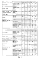
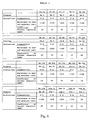
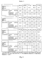
- each of the prepregs prepared in Examples 1 to 16 had excellent flexibility. Further, each of the prepregs prepared in Examples 1 to 5, 7, 9 to 13, 15, and 16 had especially little tack. Furthermore, no dust was generated from each of the prepregs prepared in Examples 1 to 3, 5, 6, and 8 to 16. Moreover, each of the prepregs prepared in Examples 15 and 16 exhibited excellent processability of via holes with laser.
- Laminates of Examples 1a to 16a were prepared using the prepregs having no metallic foil, prepared in Examples 1 to 16, respectively. 8 sheets of the prepreg were laminated, and electrodeposited copper foils having a thickness of 18 ⁇ m ("GTS" which is a product of Furukawa Circuit Foil Co., Ltd.) were overlaid respectively on both of the outermost surfaces of the laminated prepegs. Then, they were molded by heating at a temperature of 200°C under a pressure of 2.5 MPa for 90 minutes, to thereby obtain a laminate having a thickness of 0.8 mm. It is to be noted that a temperature during molding was elevated at a rate of 3°C/min from room temperature to 200°C.
- Laminates of Comparative Examples 1a to 4a were prepared using the prepregs having no metallic foil, prepared in Comparative Examples 1 to 4, respectively. 8 sheets of the prepreg were laminated, and electrodeposited copper foils having a thickness of 18 ⁇ m ("GTS" which is a product of Furukawa Circuit Foil Co., Ltd.) were overlaid respectively on both of the outermost surfaces of the laminated prepregs. Then, they were molded by heating at a temperature of 200°C under a pressure of 2.5 MPa for 90 minutes, to thereby obtain a laminate having a thickness of 0.8 mm. It is to be noted that a temperature during molding was elevated at a rate of 3°C/min from room temperature to 200°C.
- Each of the laminates was subjected to etching for stripping the metallic foil (copper foil), to thereby obtain a sample.
- the thus obtained sample was subjected to a vertical burning test in accordance with UL-94.
- a sample having a size of 50 mm ⁇ 50 mm was cut out from each of the laminates, and it was subjected to etching for stripping all the copper foil on the bottom side and half of the copper foil on the upper side, in accordance with JIS 6481, to thereby obtain a test piece.
- Each of the thus obtained test pieces was subjected to a pressure cooker at 121°C, and then was floated in a solder bath at 260°C with the copper foil being faced toward downward direction. Then, time until blister is produced was measured.
- Each of the laminates was subjected to etching for stripping the copper foil, and a test piece having a size of 2 mm ⁇ 2 mm was cut out therefrom.
- the coefficient of thermal expansion of each of the test pieces in the thickness direction (Z direction) thereof was measured using a thermal mechanical analyzer (TMA) at 5°C/min.
- each of the laminates of the Examples 1a to 16a had excellent flame retardancy, and each of the laminates of Examples 1a to 8a and 9a to 14a was V-0 level in the UL-94 burning test. Further, each of the laminates of Examples 1a to 5a, 7a, 8a, and 9a to 12a had an especially low coefficient of thermal expansion.
- Examples 1b to 16b Semiconductor packages of Examples 1b to 16b were manufactured using the prepregs with metallic foils prepared in Examples 1 to 16, respectively.
- a dry film resist ( "38A212" which is a product of Nichigo-Morton Co. , Ltd. ) was applied on the prepreg with a metallic foil, and a specified circuit pattern was exposed, and then developed by the use of a 1.5 wt% aqueous solution of sodium carbonate, to thereby form an etching resist layer.
- the prepreg with the metallic foil on which the etching resist layer (mask) was formed was subjected to etching for stripping the metallic foil, and then the etching resist layer was also stripped by the use of a 3.0 wt% aqueous solution of sodium hydroxide, to thereby form a specified conductive circuit pattern.
- a dry film solder resist (“CFP-1122" which is a product of SUMITOMO BAKELITE Co., Ltd. ) was applied on the prepreg formed with the circuit pattern so as to cover the conductive circuit pattern, and a specified solder resist pattern is exposed, and then developed by the use of a 1.5 wt% aqueous solution of sodium hydroxide, to thereby form a solder resist layer.
- via holes were made using a CO 2 laser in the resin surface of the prepreg, to thereby obtain an interposer.
- a semiconductor device was mounted in a manner described below. Specifically, a flip chip type semiconductor device having solder bumps was fed with being held by a mount tool to perform alignment between the semiconductor device and the pre-heated prepreg formed with the circuit pattern, and then the semiconductor device was mounted on the interposer. Thereafter, the mounted semiconductor device was bonded to the interposer by thermocompressing bonding at the most suitable temperature and at a pressure of 3 kg/cm 2 for 10 seconds, and the thus obtained one was then subjected to after-curing at a temperature of 200°C for 60 minutes, to thereby obtain a semiconductor package.
- Comparative Examples 3b and 4b Semiconductor packages of Comparative Examples 3b and 4b were manufactured using the prepregs with metallic foils prepared in Comparative Examples 3 and 4, respectively.
- a dry film resist manufactured by Nichigo-Morton Co., Ltd. with a product name of 38A212
- a specified circuit pattern was exposed, and then developed by the use of a 1.5 wt% aqueous solution of sodium carbonate, to thereby form an etching resist layer.
- the prepreg with the metallic foil on which the etching resist layer (mask) was formed was subjected to etching for stripping the metallic foil, and then the etching resist layer was also stripped by the use of a 3.0 wt% aqueous solution of sodium hydroxide, to thereby form a specified conductive circuit pattern.
- a dry film solder resist (manufactured by SUMITOMO BAKELITE Co. , Ltd. with a product name of CFP-1122) was applied on the thus obtained prepreg formed with the circuit pattern so as to cover the conductive circuit pattern, and a specified solder resist pattern is exposed, and then developed by the use of a 1.5 wt% aqueous solution of sodium hydroxide, to thereby form a solder resist layer.
- a semiconductor device was mounted in a manner described below. Specifically, a flip chip type semiconductor device having solder bumps was fed with it being held by a mount tool to perform alignment between the semiconductor device and the pre-heated prepreg formed with the circuit pattern, and then the semiconductor device was mounted on the interposer. Thereafter, the mounted semiconductor device was bonded to the interposer by thermocompressing bonding at the most suitable temperature and at a pressure of 3 kg/cm 2 for 10 seconds, and the thus obtained one was then subjected to after-curing at a temperature of 200°C for 60 minutes, to thereby obtain a semiconductor package.
- the semiconductor package was subjected to thermal cycling test for 1,000 cycles in the temperature range from - 40°C to 125°C with a dwell time of 30 minutes at each extreme temperature (1 hour/cycle). In this test, 10 samples were tested for each of the semiconductor packages, and measurement was made to know the number of the samples containing a broken wire after 1,000 cycles.
- each of the semiconductor packages obtained in Examples 1b to 16b was thinner than the thickness of a conventional semiconductor package by 120 ⁇ m.
- the semiconductor packages obtained in Examples 1b to 16b can be thinned, because cracking is hard to occur in the prepreg of the present invention even in the case where it is made thin. Further, since in such a thinner semiconductor package, wiring length can be shortened, high-speed operation can be achieved.
- the resin composition contains a cyanate resin having a specific molecular weight, it is possible to prevent dust from being generated from a resultant prepreg in addition to the effects described above.
- the resin composition contains a specific cyanate resin, it is possible for a resultant prepreg to have a reduced coefficient of thermal expansion in addition to the effects described above.
- the present invention it is possible to provide a prepreg having excellent flexibility and chemical resistance, and it is also possible to provide a prepreg having excellent workability even in the case where the resin composition in the prepreg is in an uncured state.
Landscapes
- Chemical & Material Sciences (AREA)
- Engineering & Computer Science (AREA)
- Materials Engineering (AREA)
- Chemical Kinetics & Catalysis (AREA)
- Manufacturing & Machinery (AREA)
- Health & Medical Sciences (AREA)
- Medicinal Chemistry (AREA)
- Polymers & Plastics (AREA)
- Organic Chemistry (AREA)
- Microelectronics & Electronic Packaging (AREA)
- Inorganic Chemistry (AREA)
- Reinforced Plastic Materials (AREA)
- Laminated Bodies (AREA)
- Compositions Of Macromolecular Compounds (AREA)
Abstract
Description

Claims (19)
- A resin composition which is used to form a sheet-shaped prepreg by being impregnated into a base material, the resin composition comprising:a first thermosetting resin having a weight average molecular weight;a second thermosetting resin having a lower weight average molecular weight than that of the first thermosetting resin;a curing agent; anda filler.
- The resin composition as claimed in claim 1, further comprising a resin of which moisture absorption is lower than that of both of the first thermosetting resin and the second thermosetting resin.
- The resin composition as claimed in claim 1, wherein the first and second thermosetting resins include epoxy resin or cyanate resin.
- The resin composition as claimed in claim 1, wherein the weight average molecular weight of the first thermosetting resin is equal to or more than 2,000.
- The resin composition as claimed in claim 1, wherein the weight average molecular weight of the second thermosetting resin is equal to or less than 1,500.
- The resin composition as claimed in claim 1, wherein at least one of the first and second thermosetting resins contains cyanate resin.
- The resin composition as claimed in claim 6, wherein the cyanate resin is a novolak-type cyanate resin.
- The resin composition as claimed in claim 1, wherein at least one of the second thermosetting resin and/or the curing agent is in a liquid state at room temperature.
- The resin composition as claimed in claim 1, wherein the filler is an inorganic filler in powder form.
- The resin composition as claimed in claim 1, wherein the filler is silica.
- The resin composition as claimed in claim 1, wherein the filler is in powder form and the average particle size of the filler is equal to or less than 2 µm.
- The resin composition as claimed in claim 1, wherein the content of the filler is 40 to 80 wt% of the total weight of the resin composition.
- A prepreg formed by impregnating a base material with the resin composition claimed in claim 1.
- The prepreg as claimed in claim 13, wherein the reaction rate of the resin composition in the prepreg is equal to or less than 30 %.
- The prepreg as claimed in claim 13, wherein the base material is a spread-out glass fiber base material.
- The prepreg as claimed in claim 13, wherein the base material is a nonwoven fabric made of organic fibers.
- A prepreg formed by laminating a metallic foil on at least one of the surfaces of the prepreg as claimed in claim 13.
- A laminate formed by laminating a metallic foil on at least one of the surfaces of the prepreg claimed in claim 13 and molding them by heating under pressure.
- A semiconductor package manufactured by mounting at least one IC chip on the prepreg claimed in claim 17.
Applications Claiming Priority (3)
| Application Number | Priority Date | Filing Date | Title |
|---|---|---|---|
| JP2001264385 | 2001-08-31 | ||
| JP2001264385 | 2001-08-31 | ||
| PCT/JP2002/008845 WO2003018675A1 (en) | 2001-08-31 | 2002-08-30 | Resin composition, prepreg, laminated sheet and semiconductor package |
Publications (2)
| Publication Number | Publication Date |
|---|---|
| EP1457515A1 true EP1457515A1 (en) | 2004-09-15 |
| EP1457515A4 EP1457515A4 (en) | 2004-11-24 |
Family
ID=19090990
Family Applications (1)
| Application Number | Title | Priority Date | Filing Date |
|---|---|---|---|
| EP02772828A Withdrawn EP1457515A4 (en) | 2001-08-31 | 2002-08-30 | RESIN COMPOSITION, PREMIX, LAMINATED SHEET, AND SEMICONDUCTOR PACKAGE |
Country Status (7)
| Country | Link |
|---|---|
| US (1) | US7368497B2 (en) |
| EP (1) | EP1457515A4 (en) |
| JP (3) | JP4133817B2 (en) |
| KR (1) | KR100920535B1 (en) |
| CN (1) | CN100422244C (en) |
| TW (1) | TWI290942B (en) |
| WO (1) | WO2003018675A1 (en) |
Cited By (3)
| Publication number | Priority date | Publication date | Assignee | Title |
|---|---|---|---|---|
| US8980417B2 (en) | 2010-04-05 | 2015-03-17 | Nitto Boseki Co., Ltd. | Process for production of glass fiber fabric having silica microparticles adhered thereon, glass fiber fabric having silica microparticles adhered thereon, and fiber-reinforced molded resin article |
| WO2015191354A1 (en) * | 2014-06-09 | 2015-12-17 | Dow Global Technologies Llc | Process for making curable, multi-layer fiber-reinforced prepreg |
| EP2832498A4 (en) * | 2012-03-30 | 2016-04-20 | Sumitomo Bakelite Co | MATERIAL FOR HOLDING A POLISHING ARTICLE AND LAMINATE PLATE USING THE MATERIAL |
Families Citing this family (34)
| Publication number | Priority date | Publication date | Assignee | Title |
|---|---|---|---|---|
| JP2005097524A (en) * | 2003-09-05 | 2005-04-14 | Sumitomo Bakelite Co Ltd | Resin composition, prepreg and laminate |
| JP4093186B2 (en) * | 2004-01-27 | 2008-06-04 | カシオ計算機株式会社 | Manufacturing method of semiconductor device |
| JP4501475B2 (en) * | 2004-03-17 | 2010-07-14 | 住友ベークライト株式会社 | Metal foil with insulating layer and multilayer printed wiring board |
| JP5085125B2 (en) * | 2004-03-29 | 2012-11-28 | 住友ベークライト株式会社 | Resin composition, metal foil with resin, insulating sheet with substrate and multilayer printed wiring board |
| JP2006273950A (en) * | 2005-03-28 | 2006-10-12 | Sumitomo Bakelite Co Ltd | Resin composition, laminated article and circuit board and method for producing circuit board |
| US20090126974A1 (en) * | 2005-09-30 | 2009-05-21 | Maroshi Yuasa | Manufacturing Process for a Prepreg with a Carrier, Prepreg with a Carrier, Manufacturing Process for a Thin Double-Sided Plate, Thin Double-Sided Plate and Manufacturing Process for a Multilayer-Printed Circuit Board |
| CN101321813B (en) * | 2005-12-01 | 2012-07-04 | 住友电木株式会社 | Prepreg, process for producing prepreg, substrate, and semiconductor device |
| KR101337168B1 (en) * | 2006-03-03 | 2013-12-05 | 스미토모 베이클리트 컴퍼니 리미티드 | Intermediate layer material, and composite laminate plate |
| US7682879B2 (en) * | 2006-03-28 | 2010-03-23 | Seagate Technology Llc | Edge coating a microelectronic device |
| WO2007126130A1 (en) * | 2006-04-28 | 2007-11-08 | Sumitomo Bakelite Co., Ltd. | Solder resist material, wiring board using the solder resist material, and semiconductor package |
| KR20090100388A (en) | 2007-01-16 | 2009-09-23 | 스미토모 베이클리트 컴퍼니 리미티드 | Multilayer printed wiring board formed by laminating the insulated resin sheet laminate and the insulated resin sheet laminate |
| CN101584259B (en) * | 2007-01-29 | 2011-09-14 | 住友电木株式会社 | Method for manufacturing laminate, substrate, substrate, and semiconductor device |
| KR20090109114A (en) | 2007-02-14 | 2009-10-19 | 스미토모 베이클리트 컴퍼니 리미티드 | Interlayer insulating film with carrier material and multilayer printed circuit board using the same |
| US8592256B2 (en) * | 2007-02-16 | 2013-11-26 | Sumitomo Bakelite Co., Ltd. | Circuit board manufacturing method, semiconductor manufacturing apparatus, circuit board and semiconductor device |
| KR100823998B1 (en) * | 2007-05-28 | 2008-04-23 | 전자부품연구원 | Manufacturing Method of Copper Clad Laminate, Printed Circuit Board and Copper Clad Laminated Plate |
| KR100910767B1 (en) * | 2007-11-13 | 2009-08-04 | 삼성정밀화학 주식회사 | Method for producing thermoplastic resin prepreg with improved impregnation and thermoplastic resin prepreg manufactured by the method |
| JP2008254451A (en) * | 2008-06-23 | 2008-10-23 | Matsushita Electric Works Ltd | Insulating sheet with metal foil |
| KR20110121616A (en) * | 2009-02-12 | 2011-11-07 | 스미토모 베이클리트 컴퍼니 리미티드 | Resin composition for wiring boards, resin sheet for wiring boards, composites, method for producing composites and semiconductor device |
| TW201204548A (en) * | 2010-02-05 | 2012-02-01 | Sumitomo Bakelite Co | Prepreg, laminate, printed wiring board, and semiconductor device |
| KR101233668B1 (en) * | 2010-12-23 | 2013-02-15 | 전자부품연구원 | The resin composition for semiconductor package substrate |
| US8823186B2 (en) | 2010-12-27 | 2014-09-02 | Shin-Etsu Chemical Co., Ltd. | Fiber-containing resin substrate, sealed substrate having semiconductor device mounted thereon, sealed wafer having semiconductor device formed thereon, a semiconductor apparatus, and method for manufacturing semiconductor apparatus |
| KR101907713B1 (en) * | 2011-03-14 | 2018-10-12 | 스미토모 베이클리트 컴퍼니 리미티드 | Prepreg for buildup |
| TW201318082A (en) * | 2011-09-02 | 2013-05-01 | Lg伊諾特股份有限公司 | Method for manufacturing substrate for chip package and method for manufacturing chip package |
| CN102676112B (en) * | 2012-06-08 | 2014-05-07 | 黑龙江省科学院石油化学研究院 | Low-temperature curing cyanate ester adhesive and preparation method thereof |
| JP6343885B2 (en) * | 2013-08-02 | 2018-06-20 | 味の素株式会社 | Manufacturing method of multilayer printed wiring board |
| JP6277543B2 (en) * | 2013-11-27 | 2018-02-14 | パナソニックIpマネジメント株式会社 | Composite laminate and method for manufacturing the same |
| US10655018B2 (en) | 2014-04-03 | 2020-05-19 | Lg Chem, Ltd. | Silica sol composition having excellent dispersibility in cyanate-based resin and method for preparing same |
| CN104191794B (en) * | 2014-09-18 | 2015-12-30 | 苏州生益科技有限公司 | A kind of preparation method of laminated board |
| FI128003B (en) | 2016-03-24 | 2019-07-31 | Metsaeliitto Osuuskunta | Method of manufacturing a wood veneer product and a wood veneer product thus obtained |
| US11040517B2 (en) * | 2016-11-09 | 2021-06-22 | Showa Denko Materials Co., Ltd. | Printed wiring board and semiconductor package |
| JP6928908B2 (en) * | 2017-04-07 | 2021-09-01 | パナソニックIpマネジメント株式会社 | Prepreg, metal-clad laminate, printed wiring board and flex rigid printed wiring board |
| CN110181903B (en) * | 2019-06-06 | 2021-04-13 | 江门建滔电子发展有限公司 | High-frequency high-speed copper-clad plate and preparation method thereof |
| CN111690231A (en) * | 2020-06-08 | 2020-09-22 | 安徽宏飞钓具有限公司 | Preparation method of military product outer package based on high-performance fiber composite material |
| JP7739891B2 (en) | 2021-09-22 | 2025-09-17 | 富士フイルムビジネスイノベーション株式会社 | Toner for developing electrostatic images, electrostatic image developer, toner cartridge, process cartridge, image forming apparatus, and image forming method |
Family Cites Families (30)
| Publication number | Priority date | Publication date | Assignee | Title |
|---|---|---|---|---|
| JPS6037810B2 (en) * | 1978-12-08 | 1985-08-28 | 東邦レーヨン株式会社 | Strand prepreg composition |
| JPS61209234A (en) | 1985-03-14 | 1986-09-17 | Matsushita Electric Works Ltd | Epoxy resin laminate |
| JPS62169828A (en) * | 1986-01-22 | 1987-07-27 | Teijin Ltd | Production of substrate for printed circuit |
| JPH01245038A (en) * | 1988-03-27 | 1989-09-29 | Matsushita Electric Works Ltd | Method for impregnating resin containing inorganic substance particle dispersed therein |
| US5548034A (en) | 1992-07-31 | 1996-08-20 | International Business Machines Corporation | Modified dicyanate ester resins having enhanced fracture toughness |
| JP3309661B2 (en) * | 1995-08-14 | 2002-07-29 | 信越化学工業株式会社 | Epoxy resin composition and semiconductor device |
| JP3724024B2 (en) * | 1995-11-13 | 2005-12-07 | 大日本インキ化学工業株式会社 | Epoxy resin composition for laminates |
| JPH09255800A (en) * | 1996-03-25 | 1997-09-30 | Toray Ind Inc | Prepreg and fiber reinforced resin molding |
| JPH10330513A (en) * | 1997-06-02 | 1998-12-15 | Toray Ind Inc | Prepreg and fiber reinforced composite material |
| JPH1112463A (en) * | 1997-06-27 | 1999-01-19 | Hitachi Chem Co Ltd | Resin composition for printed circuit board, varnish, prepreg, and laminate for printed circuit board prepared therefrom |
| JPH11158752A (en) * | 1997-11-26 | 1999-06-15 | Asahi Schwebel Co Ltd | Glass cloth |
| JPH11171972A (en) * | 1997-12-08 | 1999-06-29 | Toray Ind Inc | Epoxy resin composition for fiber reinforced composite material, prepreg and fiber reinforced composite material |
| JPH11172076A (en) * | 1997-12-08 | 1999-06-29 | Toray Ind Inc | Epoxy resin composition for fiber reinforced composite material, prepreg and fiber reinforced composite material |
| JPH11181123A (en) * | 1997-12-25 | 1999-07-06 | Sumitomo Bakelite Co Ltd | Prepreg |
| JPH11228670A (en) * | 1998-02-19 | 1999-08-24 | Hitachi Chem Co Ltd | Epoxy resin composition, epoxy resin prepreg, epoxy resin laminate and metal-clad epoxy resin laminate |
| JPH11343398A (en) * | 1998-03-31 | 1999-12-14 | Hitachi Chem Co Ltd | Flame retardant epoxy resin composition, and prepreg, laminate for electrical wiring board and metallic foil with resin using the composition |
| JP2000216512A (en) * | 1999-01-27 | 2000-08-04 | Hitachi Chem Co Ltd | Manufacture of printed wiring board |
| JP2000273222A (en) * | 1999-03-26 | 2000-10-03 | Sumitomo Bakelite Co Ltd | Flame-retardant prepreg and laminate |
| JP3877261B2 (en) * | 1999-06-03 | 2007-02-07 | 住友ベークライト株式会社 | Flame retardant resin composition, prepreg and laminate using the same |
| JP2001081305A (en) * | 1999-09-16 | 2001-03-27 | Asahi Kasei Corp | Curable polyphenylene ether-based resin composition |
| JP4423779B2 (en) * | 1999-10-13 | 2010-03-03 | 味の素株式会社 | Epoxy resin composition, adhesive film and prepreg using the composition, multilayer printed wiring board using the same, and method for producing the same |
| JP2001156461A (en) | 1999-11-30 | 2001-06-08 | Mitsubishi Gas Chem Co Inc | Build-up multilayer printed wiring board |
| JP4156180B2 (en) * | 2000-07-10 | 2008-09-24 | 住友ベークライト株式会社 | Epoxy resin composition, prepreg, and copper-clad laminate using the same |
| JP2002105198A (en) | 2000-10-02 | 2002-04-10 | Mitsubishi Gas Chem Co Inc | Non-halogen high adhesion flame retardant cyanate resin composition |
| JP4780361B2 (en) | 2000-10-06 | 2011-09-28 | 株式会社豊田中央研究所 | Lithium secondary battery |
| JP2002114838A (en) | 2000-10-10 | 2002-04-16 | Mitsubishi Gas Chem Co Inc | Highly durable flame retardant cyanate resin |
| JP2002114823A (en) | 2000-10-10 | 2002-04-16 | Mitsubishi Gas Chem Co Inc | Flame-retardant cyanate resin for high-frequency use |
| JP2002172736A (en) * | 2000-12-04 | 2002-06-18 | Hitachi Chem Co Ltd | Metal foil-clad laminated sheet |
| JP4738622B2 (en) * | 2001-04-13 | 2011-08-03 | 住友ベークライト株式会社 | Heat resistant resin composition, prepreg and laminate using the same |
| JP2003206360A (en) * | 2002-01-16 | 2003-07-22 | Sumitomo Bakelite Co Ltd | Prepreg and printed wiring board prepared therefrom |
-
2002
- 2002-08-30 KR KR1020047002910A patent/KR100920535B1/en not_active Expired - Fee Related
- 2002-08-30 EP EP02772828A patent/EP1457515A4/en not_active Withdrawn
- 2002-08-30 CN CNB028212975A patent/CN100422244C/en not_active Expired - Fee Related
- 2002-08-30 WO PCT/JP2002/008845 patent/WO2003018675A1/en not_active Ceased
- 2002-08-30 JP JP2003523530A patent/JP4133817B2/en not_active Expired - Fee Related
- 2002-09-02 TW TW091119921A patent/TWI290942B/en not_active IP Right Cessation
-
2004
- 2004-02-27 US US10/789,914 patent/US7368497B2/en not_active Expired - Fee Related
-
2010
- 2010-04-23 JP JP2010099840A patent/JP5573331B2/en not_active Expired - Fee Related
-
2011
- 2011-10-17 JP JP2011227550A patent/JP2012031428A/en active Pending
Cited By (3)
| Publication number | Priority date | Publication date | Assignee | Title |
|---|---|---|---|---|
| US8980417B2 (en) | 2010-04-05 | 2015-03-17 | Nitto Boseki Co., Ltd. | Process for production of glass fiber fabric having silica microparticles adhered thereon, glass fiber fabric having silica microparticles adhered thereon, and fiber-reinforced molded resin article |
| EP2832498A4 (en) * | 2012-03-30 | 2016-04-20 | Sumitomo Bakelite Co | MATERIAL FOR HOLDING A POLISHING ARTICLE AND LAMINATE PLATE USING THE MATERIAL |
| WO2015191354A1 (en) * | 2014-06-09 | 2015-12-17 | Dow Global Technologies Llc | Process for making curable, multi-layer fiber-reinforced prepreg |
Also Published As
| Publication number | Publication date |
|---|---|
| US20040234741A1 (en) | 2004-11-25 |
| JP2010215911A (en) | 2010-09-30 |
| CN100422244C (en) | 2008-10-01 |
| KR100920535B1 (en) | 2009-10-08 |
| CN1608100A (en) | 2005-04-20 |
| JP2012031428A (en) | 2012-02-16 |
| HK1077313A1 (en) | 2006-02-10 |
| KR20040029080A (en) | 2004-04-03 |
| TWI290942B (en) | 2007-12-11 |
| JP5573331B2 (en) | 2014-08-20 |
| JP4133817B2 (en) | 2008-08-13 |
| US7368497B2 (en) | 2008-05-06 |
| EP1457515A4 (en) | 2004-11-24 |
| WO2003018675A1 (en) | 2003-03-06 |
| JPWO2003018675A1 (en) | 2004-12-09 |
Similar Documents
| Publication | Publication Date | Title |
|---|---|---|
| US7368497B2 (en) | Resin composition, prepreg, laminate, and semiconductor package | |
| US8465837B2 (en) | Epoxy resin composition, prepreg, laminate board, multilayer printed wiring board, semiconductor device, insulating resin sheet, and process for manufacturing multilayer printed wiring board | |
| JP5522051B2 (en) | Multilayer printed wiring board and semiconductor device | |
| KR101355777B1 (en) | Prepreg, laminate, printed wiring board, and semiconductor device | |
| KR101502653B1 (en) | Laminate, circuit board and semiconductor device | |
| EP2180772A1 (en) | Multilayered wiring board and semiconductor device | |
| KR20110091458A (en) | Prepregs, laminates, printed wiring boards and semiconductor devices | |
| JP5206600B2 (en) | Epoxy resin composition, prepreg, laminate, resin sheet, multilayer printed wiring board, and semiconductor device | |
| JP2010174242A (en) | Biphenyl aralkyl type cyanate ester resin, resin composition containing biphenyl aralkyl type cyanate ester resin, and prepreg, laminated plate, resin sheet, multilayer printed wiring board, and semiconductor device obtained using the resin composition | |
| JP2004182851A (en) | Resin composition, prepreg, and printed wiring board therewith | |
| JP4322463B2 (en) | Copper-clad laminate prepreg and copper-clad laminate | |
| JP2003253018A (en) | Prepreg and printed wiring board using the same | |
| JP2009298981A (en) | Resin composition, prepreg and printed wiring board using the same | |
| JP5448414B2 (en) | Resin composition, prepreg, laminate, multilayer printed wiring board, and semiconductor device | |
| JP4840303B2 (en) | Insulated resin sheet with glass fiber woven fabric, laminated board, multilayer printed wiring board, and semiconductor device | |
| JP4552496B2 (en) | Resin composition, prepreg, laminate and semiconductor package | |
| JP4466590B2 (en) | Resin composition, prepreg, laminate and semiconductor package | |
| JP4385555B2 (en) | Interposer, semiconductor package and manufacturing method thereof | |
| JP5194423B2 (en) | Resin composition, prepreg, laminate, and semiconductor device | |
| JP2010080609A (en) | Semiconductor device | |
| WO2013099771A1 (en) | Prepreg, circuit board and semiconductor device | |
| JP2006176790A (en) | Metal-foil-fitted prepreg, laminate, and semiconductor package | |
| HK1077313B (en) | Resin composition, prepreg, laminated sheet and semiconductor package | |
| JP2009302554A (en) | Prepreg with metal foil, laminate sheet, and interposer |
Legal Events
| Date | Code | Title | Description |
|---|---|---|---|
| PUAI | Public reference made under article 153(3) epc to a published international application that has entered the european phase |
Free format text: ORIGINAL CODE: 0009012 |
|
| 17P | Request for examination filed |
Effective date: 20040218 |
|
| AK | Designated contracting states |
Kind code of ref document: A1 Designated state(s): AT BE BG CH CY CZ DE DK EE ES FI FR GB GR IE IT LI LU MC NL PT SE SK TR |
|
| AX | Request for extension of the european patent |
Extension state: AL LT LV MK RO SI |
|
| A4 | Supplementary search report drawn up and despatched |
Effective date: 20041012 |
|
| RIC1 | Information provided on ipc code assigned before grant |
Ipc: 7C 08L 79/00 B Ipc: 7C 08L 63/00 B Ipc: 7C 08L 101/00 B Ipc: 7H 05K 1/03 B Ipc: 7C 08J 5/24 A |
|
| STAA | Information on the status of an ep patent application or granted ep patent |
Free format text: STATUS: THE APPLICATION IS DEEMED TO BE WITHDRAWN |
|
| 18D | Application deemed to be withdrawn |
Effective date: 20070301 |