EP1456951B1 - Halbbrückentreiber und stromwandlersystem mit einem solchen treiber - Google Patents
Halbbrückentreiber und stromwandlersystem mit einem solchen treiber Download PDFInfo
- Publication number
- EP1456951B1 EP1456951B1 EP02779847A EP02779847A EP1456951B1 EP 1456951 B1 EP1456951 B1 EP 1456951B1 EP 02779847 A EP02779847 A EP 02779847A EP 02779847 A EP02779847 A EP 02779847A EP 1456951 B1 EP1456951 B1 EP 1456951B1
- Authority
- EP
- European Patent Office
- Prior art keywords
- current
- bridge driver
- driver according
- output
- voltage
- Prior art date
- Legal status (The legal status is an assumption and is not a legal conclusion. Google has not performed a legal analysis and makes no representation as to the accuracy of the status listed.)
- Expired - Lifetime
Links
- 238000006243 chemical reaction Methods 0.000 title claims description 9
- 239000000872 buffer Substances 0.000 claims description 19
- 230000005669 field effect Effects 0.000 claims description 2
- 230000001939 inductive effect Effects 0.000 claims description 2
- 229910052710 silicon Inorganic materials 0.000 claims description 2
- 239000010703 silicon Substances 0.000 claims description 2
- XUIMIQQOPSSXEZ-UHFFFAOYSA-N Silicon Chemical compound [Si] XUIMIQQOPSSXEZ-UHFFFAOYSA-N 0.000 claims 1
- 239000000758 substrate Substances 0.000 claims 1
- 238000010586 diagram Methods 0.000 description 5
- 238000001914 filtration Methods 0.000 description 2
- 230000006870 function Effects 0.000 description 2
- 230000001965 increasing effect Effects 0.000 description 2
- 230000003071 parasitic effect Effects 0.000 description 2
- 230000003321 amplification Effects 0.000 description 1
- 230000009977 dual effect Effects 0.000 description 1
- 230000005520 electrodynamics Effects 0.000 description 1
- 230000008030 elimination Effects 0.000 description 1
- 238000003379 elimination reaction Methods 0.000 description 1
- 230000036039 immunity Effects 0.000 description 1
- 238000000034 method Methods 0.000 description 1
- 238000003199 nucleic acid amplification method Methods 0.000 description 1
- 230000000630 rising effect Effects 0.000 description 1
Images


Classifications
-
- H—ELECTRICITY
- H03—ELECTRONIC CIRCUITRY
- H03K—PULSE TECHNIQUE
- H03K17/00—Electronic switching or gating, i.e. not by contact-making and –breaking
- H03K17/51—Electronic switching or gating, i.e. not by contact-making and –breaking characterised by the components used
- H03K17/56—Electronic switching or gating, i.e. not by contact-making and –breaking characterised by the components used by the use, as active elements, of semiconductor devices
- H03K17/687—Electronic switching or gating, i.e. not by contact-making and –breaking characterised by the components used by the use, as active elements, of semiconductor devices the devices being field-effect transistors
- H03K17/6871—Electronic switching or gating, i.e. not by contact-making and –breaking characterised by the components used by the use, as active elements, of semiconductor devices the devices being field-effect transistors the output circuit comprising more than one controlled field-effect transistor
-
- H—ELECTRICITY
- H03—ELECTRONIC CIRCUITRY
- H03K—PULSE TECHNIQUE
- H03K5/00—Manipulating of pulses not covered by one of the other main groups of this subclass
- H03K5/125—Discriminating pulses
- H03K5/1252—Suppression or limitation of noise or interference
-
- H—ELECTRICITY
- H03—ELECTRONIC CIRCUITRY
- H03K—PULSE TECHNIQUE
- H03K17/00—Electronic switching or gating, i.e. not by contact-making and –breaking
- H03K17/06—Modifications for ensuring a fully conducting state
- H03K17/063—Modifications for ensuring a fully conducting state in field-effect transistor switches
Definitions
- the present invention relates to a half-bridge power stage driver, comprising first and second power switches, connected with their respective current paths in series, a pulse generator for generating a voltage pulse waveform, arranged to drive said first power switch, a first current generator, for generating a current pulse for each trailing edge of said voltage pulse waveform, and a second current generator, for generating a current pulse for each leading edge of said voltage pulse waveform.
- the invention can advantageously be used in power conversion systems where high-speed operation, combined with low power consumption is required as e.g. motor drive and in particular in power amplification for audio use.
- a half-bridge is a power converter comprising two power switches, e.g. transistors, one referred to as the low side transistor, and the other referred to as the high side transistor. Each transistor is driven by separate drive circuits, i.e. a low side driver and a high side driver.
- controlling systems for a high side driver comprise a pulse technique, where narrow set and reset current pulses are transmitted to the high side driver, in which a latch is placed to restore the original control signal.
- a pulse technique where narrow set and reset current pulses are transmitted to the high side driver, in which a latch is placed to restore the original control signal.
- the current pulses have been converted into voltage pulses in the high side driver by means of two pull up resistors. This approach does not in it self provide any common mode rejection and additionally circuits have been mandatory.
- pull up resistors In general, the use of pull up resistors is not suitable for logic level driver voltage because of the negative load terminal voltage that must be expected to compromise the logic level of the high side set/reset inputs.
- An object of the present invention is to provide a novel system for receiving and handling the set and reset current pulses in a high side driver, thereby obtaining reliable operating conditions for operating the power switching transistors.
- a second object of the invention is to provide a half-bridge driver with cancellation of common mode currents.
- a half bridge driver of the kind mentioned by way of introduction further comprising a differential current receiver circuit, having at least one low impedance current buffer connected to said first and second current generators, said differential current receiver circuit arranged to generate an output signal equal to the difference of the currents flowing through said current generators, said output signal arranged to drive said second power switch.
- the set and reset current pulses are received by low impedance non-inverting and inverting current buffers respectively.
- the output of these buffers are then connected and summed.
- summating the common mode noise currents induced by the dv/dt in the set and reset current paths one current will be inverted so that the currents cancel, and false triggering is prevented.
- the pulse generated signals stay as currents that are insensitive to capacitances, and also the driver is immune to negative offset voltages. Further, it is now possible to reduce the required drive voltage, thereby reducing power consumption and operating temperatures for the half-bridge driver.
- the low impedance inputs result in elimination of voltage swings on the inputs and the dc bias point of these inputs will be as close as possible to the positive power supply of the high side driver. This will enable the level shift to show secure function even for high negative offset voltages because the decision points is no longer based on voltage drops across the prior pull up resistors. This feature is of great benefit in terms of power reduction, because it enables lowering of the operating voltage of the driver. This enables reduction of power dissipation, a reduction of the die size and an increase in the speed performance.
- a logic buffer with a feedback resistor can be arranged, acting as memory cell.
- the restored control signal for the gate drive is then found on the output of the memory cell.
- the value of the resistor and the threshold of the buffer determine the magnitude of the current for flipping the latch. Thereby, common mode currents are cancelled and common mode rejection of noise is achieved.
- FIG. 1 is a schematic diagram of a prior art implementation of a pulse control of a high side driver.
- FIG. 2 is a diagram with common time base showing the timing of the system in fig 1 .
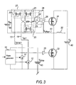
- FIG. 3 is a schematic diagram of a half-bridge driver according to a preferred embodiment of the invention.
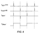
- FIG. 4 is a diagram showing the current pulses in the system in fig 3 .
- FIG. 1 A topology for an output stage is illustrated in FIG. 1 .
- the driver has two pull-up resistors 1, 2, a filter or gate block 4 for noise rejection, and a latch 3.
- the system further comprises current generators 11, 12 controlled by a pulse generator 10.
- the output stage comprises two N-channel power switches 31 and 33.
- the load terminal is referred to as V offset 41.
- the output terminals, 41 and ground or -V d can drive any type of load, for example an inductive load such as a coil or an electro-dynamic transducer.
- the offset voltage is also the reference potential for the high-side driver and will under normal operation be OV or ⁇ V d 42.
- the high side driver is powered from the supply V bs 40 and this voltage preferably equals the supply V d 42.
- FIG. 2 shows the timing of the system.
- the current generators 11, 12 generate narrow current pulses at the rising and trailing edges of the voltage pulse waveform generated by the pulse generator 10 . This produces narrow voltage pulses over the resistors 1 and 2 for respectively setting and resetting of the latch 3 , which through a driver 26 provides a gate control signal for the floating switch device.
- the first preferred embodiment of the invention is shown in FIG. 3 , where components similar to the components in fig 1 have been given identical reference numerals.
- the current generators 11, 12 and the pulse generator 10 can be implemented as any given generator topology.
- the power switches 31 and 33 can be any type of transistor, preferably a type of transistor optimized for operating in an "on" or "off” state such as a Field Effect Transistor.
- the power supply V d 42 as shown in Fig. 3 is a single (+ and reference to ground) voltage power supply.
- the circuit nodes fixed to ground can be replaced by negative supply circuit nodes so that the low side driver uses the negative supply as a reference and a dual ( ⁇ ) V d supply 42 can be used.
- the half-bridge driver in fig 3 comprises a current receiver circuit 27, having a plurality of low impedance input current buffers.
- these low impedance current buffers are implemented as current mirrors 20, 21, 23, based on MOSFET transistors.
- the current buffers 20, 21, 23 are connected to the voltage supply V bs according to fig 3 .
- the driver also includes a memory cell 28, comprising a logic buffer 25 and a positive feedback resistor 24, connected to the driver 26.
- the current generators 11, 12 are connected to the mirrors 20 and 21 respectively, while the mirrors 21 and 23 are connected to the memory cell 28.
- voltage pulse waveforms are generated by the pulse generator 10 and transformed into current pulses by current generators 11 and 12.
- the first current generator 11 generates a pulse I RESET for each trailing edge of the voltage pulse
- the second current generator 12 generates a pulse I SET for each leading edge of the voltage pulse.
- These current pulses are received by the current mirrors 20 and 21 respectively, in the current receiver circuit 27.
- the mirrored reset current pulse I RESET is supplied from the current mirror 20 to the current mirror 23, where it is again mirrored.
- the outputs from current mirrors 21 and 23 are summed at the input terminal of the buffer 25.
- the set current pulse I SET causes a current pulse of same magnitude and direction in the point referred to as I LATCH in fig 3 .
- the current flows into the memory cell 28.
- Said I LATCH current is converted into a voltage across the positive feedback resistor 24, causing the memory cell 28 to go into high state.
- a reset current pulse I RESET is received, a current of same magnitude but opposite direction will flow in the positive feedback resistor 24, resulting in a reset of the memory cell.
- FIG. 4 an example of a common mode noise situation is illustrated as a set and reset pulse occurring at the same time. In this situation these two currents simply cancel each other obtaining common mode current rejection. This is obtained since the current flowing through the feedback resistor 24 is zero, therefore there will not be a voltage drop across it.
- the half-bridge driver can be implemented in any given power conversion system comprising a half-bridge of transistors such as DC-DC, AC-AC, DC-AC, AC-DC power conversion systems or any combination of the above mentioned.
- the half-bridge driver can be implemented in high precision DC-AC power conversion systems comprising one or a plurality of half-bridges and one or a plurality of half-bridge drivers.
- the half-bridge driver can be implemented on silicon thus reducing size and increasing performance in terms of speed and precision of the half-bridge driver.
Landscapes
- Physics & Mathematics (AREA)
- Nonlinear Science (AREA)
- Electronic Switches (AREA)
- Amplifiers (AREA)
- Power Conversion In General (AREA)
- Diaphragms For Electromechanical Transducers (AREA)
- Automatic Cycles, And Cycles In General (AREA)
- Coils Or Transformers For Communication (AREA)
Claims (14)
- Halbbrückentreiber, der Folgendes umfasst:einen ersten und einen zweiten Leistungsschalter, die mit ihren jeweiligen Strompfaden in Reihe geschaltet sind,einen Impulsgenerator zum Erzeugen einer Spannungsimpulswellenform, der dafür ausgelegt ist, den ersten Leistungsschalter (33) anzusteuern,einen ersten Stromgenerator (11) zum Erzeugen eines ersten Stromsignals, das einen Stromimpuls für jede negative Flanke der Spannungsimpulswellenform enthält,einen zweiten Stromgenerator (12) zum Erzeugen eines zweiten Stromsignals, das einen Stromimpuls für jede positive Flanke der Spannungsimpulswellenform enthält, undeinen Differenzstromempfängerschaltkreis (27), der mit dem ersten und dem zweiten Stromgenerator verbunden ist und dafür ausgelegt ist, ein Ausgangsstromsignal (ILatch) zu erzeugen, das gleich der Differenz zwischen dem ersten und dem zweiten Stromsignal, die durch die Stromgeneratoren (11, 12) erzeugt werden, ist,wobei das Ausgangsstromsignal dafür ausgelegt ist, den zweiten Leistungsschalter (31) anzusteuern.
- Halbbrückentreiber nach Anspruch 1, wobei der Differenzstromempfängerschaltkreis (27) mindestens einen Niedrigimpedanz-Strompuffer (20, 21, 23) umfasst.
- Halbbrückentreiber nach Anspruch 1, wobei der Differenzstromempfängerschaltkreis (27) drei Niedrigimpedanz-Strompuffer (20, 21, 23) umfasst.
- Halbbrückentreiber nach Anspruch 2 oder 3, wobei mindestens einer der Strompuffer ein Stromspiegelschaltkreis (20, 21, 23) ist.
- Halbbrückentreiber nach einem der vorangehenden Ansprüche, der des Weiteren eine Speicherzelle (28) umfasst, die einen Puffer (25) und einen Rückkopplungswiderstand (24) aufweist, wobei die Speicherzelle mit dem Ausgangssignal (ILatch) verbunden ist.
- Halbbrückentreiber nach einem der vorangehenden Ansprüche, wobei die Leistungsschalter Transistoren (31, 33), wie zum Beispiel Feldeffekt-Transistoren, sind.
- Halbbrückentreiber nach einem der vorangehenden Ansprüche, der des Weiteren zwei Spannungsquellen (40, 42) umfasst, die vorzugsweise die gleiche Spannungsgrößenordnung abgeben.
- Halbbrückentreiber nach einem der vorangehenden Ansprüche, der des Weiteren einen Logikpegelspannungsbetrieb mit einer Logikpegelspannung von 0-5 Volt aufweist.
- Halbbrückentreiber nach einem der vorangehenden Ansprüche, der auf Siliziumsubstraten implementiert ist.
- Leistungswandlungssystem zum Ansteuern einer induktiven Last, das einen Halbbrückentreiber nach einem der vorangehenden Ansprüche umfasst.
- Leistungswandlungssystem nach Anspruch 10, das mehrere Halbbrückentreiber nach einem der vorangehenden Ansprüche umfasst.
- Leistungswandlungssystem nach Anspruch 10 oder 11, das zur Gleichstrom-Wechselstrom-Audioleistungswandlung verwendet wird.
- Halbbrückentreiber nach Anspruch 1, der des Weiteren Folgendes umfasst:einen ersten invertierenden Niedrigimpedanz-Strompuffer (20, 23), der dafür ausgelegt ist, das erste Stromsignal zu empfangen,einen zweiten nicht-invertierenden Niedrigimpedanz-Strompuffer (21) der dafür ausgelegt ist, das erste Stromsignal zu empfangen,einen Puffer (25), der dafür ausgelegt ist, Ausgangssignale des ersten und des zweiten Strompuffers zu summieren und das Ausgangsstromsignal auszugeben.
- Halbbrückentreiber nach Anspruch 1, der des Weiteren Folgendes umfasst:einen ersten Stromspiegel (20), der dafür ausgelegt ist, das erste Stromsignal zu empfangen,einen zweiten Stromspiegel (21), der dafür ausgelegt ist, das zweite Stromsignal zu empfangen,einen dritten Stromspiegel (23), der dafür ausgelegt ist, ein Ausgangssignal des ersten Stromspiegels zu empfangen,einen Puffer (25), der dafür ausgelegt ist, Ausgangssignale des ersten und des dritten Stromspiegels (20, 23) zu summieren und das Ausgangsstromsignal auszugeben.
Applications Claiming Priority (3)
| Application Number | Priority Date | Filing Date | Title |
|---|---|---|---|
| SE0104400 | 2001-12-21 | ||
| SE0104400A SE0104400D0 (sv) | 2001-12-21 | 2001-12-21 | Half-bridge driver and power conversion system with such driver |
| PCT/IB2002/005152 WO2003055072A1 (en) | 2001-12-21 | 2002-12-05 | Half-bridge driver and power conversion system with such driver |
Publications (2)
| Publication Number | Publication Date |
|---|---|
| EP1456951A1 EP1456951A1 (de) | 2004-09-15 |
| EP1456951B1 true EP1456951B1 (de) | 2010-01-20 |
Family
ID=20286496
Family Applications (1)
| Application Number | Title | Priority Date | Filing Date |
|---|---|---|---|
| EP02779847A Expired - Lifetime EP1456951B1 (de) | 2001-12-21 | 2002-12-05 | Halbbrückentreiber und stromwandlersystem mit einem solchen treiber |
Country Status (11)
| Country | Link |
|---|---|
| US (1) | US7323912B2 (de) |
| EP (1) | EP1456951B1 (de) |
| JP (1) | JP4235561B2 (de) |
| KR (1) | KR100933651B1 (de) |
| CN (1) | CN1248415C (de) |
| AT (1) | ATE456187T1 (de) |
| AU (1) | AU2002343177A1 (de) |
| DE (1) | DE60235197D1 (de) |
| ES (1) | ES2338304T3 (de) |
| SE (1) | SE0104400D0 (de) |
| WO (1) | WO2003055072A1 (de) |
Families Citing this family (31)
| Publication number | Priority date | Publication date | Assignee | Title |
|---|---|---|---|---|
| CN1723601A (zh) * | 2002-12-10 | 2006-01-18 | 皇家飞利浦电子股份有限公司 | 集成的半桥功率电路 |
| KR100568107B1 (ko) * | 2003-10-24 | 2006-04-05 | 삼성전자주식회사 | 고속 및 저전력 전압 레벨 변환 회로 |
| KR100600452B1 (ko) * | 2004-12-29 | 2006-07-13 | 한국전기연구원 | 펄스 발생기를 위한 반도체 스위치 구동회로 |
| WO2007003967A2 (en) | 2005-07-06 | 2007-01-11 | Cambridge Semiconductor Limited | Switch mode power supply control systems |
| DE602005005822T2 (de) * | 2005-09-29 | 2009-04-30 | Infineon Technologies Ag | Schaltkreis und adaptives Verfahren zum Antrieb einer Halbbrückenschaltung |
| GB2433363A (en) * | 2005-12-16 | 2007-06-20 | Cambridge Semiconductor Ltd | A high side transistor drive circuit |
| US7710098B2 (en) | 2005-12-16 | 2010-05-04 | Cambridge Semiconductor Limited | Power supply driver circuit |
| US7733098B2 (en) | 2005-12-22 | 2010-06-08 | Cambridge Semiconductor Limited | Saturation detection circuits |
| US20070223154A1 (en) * | 2006-03-21 | 2007-09-27 | Christian Locatelli | High side reset logic for gate driver |
| US7986926B2 (en) * | 2006-09-27 | 2011-07-26 | Silicon Laboratories Inc. | Integrating an FM transmitter into a cellular telephone |
| KR100750734B1 (ko) * | 2006-10-26 | 2007-08-22 | 삼성전자주식회사 | 광원구동회로 및 구동방법 |
| JP5082574B2 (ja) * | 2007-05-07 | 2012-11-28 | 三菱電機株式会社 | 半導体装置 |
| US8044699B1 (en) * | 2010-07-19 | 2011-10-25 | Polar Semiconductor, Inc. | Differential high voltage level shifter |
| US8405422B2 (en) * | 2010-09-30 | 2013-03-26 | Fuji Electric Co., Ltd. | Level shift circuit |
| CN102468828B (zh) * | 2010-11-03 | 2017-11-28 | 北京普源精电科技有限公司 | 一种波形发生器的脉冲边沿调控装置 |
| KR101350545B1 (ko) * | 2012-05-31 | 2014-01-13 | 삼성전기주식회사 | 레벨 변환 회로 및 그를 포함하는 게이트 드라이버 회로 |
| US8633745B1 (en) * | 2012-08-30 | 2014-01-21 | Allegro Microsystems, Llc | Circuits and related techniques for driving a high side of a half bridge circuit |
| US9509300B2 (en) | 2013-05-24 | 2016-11-29 | Dialog Semiconductor Gmbh | Anti-shoot-through automatic multiple feedback gate drive control circuit |
| US9960620B2 (en) * | 2014-09-16 | 2018-05-01 | Navitas Semiconductor, Inc. | Bootstrap capacitor charging circuit for GaN devices |
| US9780639B2 (en) * | 2015-01-19 | 2017-10-03 | Infineon Technologies Austria Ag | Protection from hard commutation events at power switches |
| US10116301B2 (en) * | 2016-07-12 | 2018-10-30 | Infineon Technologies Americas Corp. | Cross-coupled, narrow pulse, high voltage level shifting circuit with voltage domain common mode rejection |
| US10230356B2 (en) | 2017-02-27 | 2019-03-12 | Allegro Microsystems, Llc | High-side output transistor circuit |
| US10498212B2 (en) * | 2017-05-26 | 2019-12-03 | Dialog Semiconductor (Uk) Limited | Gate driver |
| US10355674B2 (en) * | 2017-07-24 | 2019-07-16 | Arm Limited | Clock gating circuit |
| US10164618B1 (en) * | 2017-12-28 | 2018-12-25 | Micron Technology, Inc. | Jitter cancellation with automatic performance adjustment |
| US10833672B2 (en) * | 2018-11-15 | 2020-11-10 | Rohm Co., Ltd. | Driving circuit for high-side transistor, switching circuit, and controller for DC/DC converter |
| CN112118003B (zh) * | 2020-08-19 | 2025-03-07 | 苏州锴威特半导体股份有限公司 | 一种电平位移电路 |
| JP2022144130A (ja) * | 2021-03-18 | 2022-10-03 | ローム株式会社 | ハイサイドトランジスタの駆動回路、スイッチング回路、dc/dcコンバータのコントローラ |
| CN115632553B (zh) * | 2022-10-31 | 2025-12-16 | 西安微电子技术研究所 | 一种快速导通的高压驱动半桥电路 |
| US12580570B2 (en) | 2023-11-29 | 2026-03-17 | Infineon Technologies Austria Ag | Level shifter having a cross-coupled current mirror circuit for reducing or cancelling common mode slew current |
| US12597928B2 (en) * | 2024-03-11 | 2026-04-07 | Infineon Technologies Austria Ag | Level shifter for power electronics circuits |
Family Cites Families (8)
| Publication number | Priority date | Publication date | Assignee | Title |
|---|---|---|---|---|
| US5283477A (en) * | 1989-08-31 | 1994-02-01 | Sharp Kabushiki Kaisha | Common driver circuit |
| US4994955A (en) | 1989-12-29 | 1991-02-19 | North American Philips Corporation | Half-bridge driver which is insensitive to common mode currents |
| US5105099A (en) | 1991-03-01 | 1992-04-14 | Harris Corporation | Level shift circuit with common mode rejection |
| US5666280A (en) * | 1993-05-07 | 1997-09-09 | Philips Electronics North America Corporation | High voltage integrated circuit driver for half-bridge circuit employing a jet to emulate a bootstrap diode |
| US5418495A (en) | 1994-05-18 | 1995-05-23 | Elantec | Input stage improvement for current feedback amplifiers |
| US5514981A (en) | 1994-07-12 | 1996-05-07 | International Rectifier Corporation | Reset dominant level-shift circuit for noise immunity |
| US6353345B1 (en) * | 2000-04-04 | 2002-03-05 | Philips Electronics North America Corporation | Low cost half bridge driver integrated circuit with capability of using high threshold voltage DMOS |
| JP3838083B2 (ja) * | 2001-12-10 | 2006-10-25 | サンケン電気株式会社 | レベルシフト回路 |
-
2001
- 2001-12-21 SE SE0104400A patent/SE0104400D0/xx unknown
-
2002
- 2002-12-05 CN CNB028257979A patent/CN1248415C/zh not_active Expired - Fee Related
- 2002-12-05 DE DE60235197T patent/DE60235197D1/de not_active Expired - Lifetime
- 2002-12-05 AT AT02779847T patent/ATE456187T1/de not_active IP Right Cessation
- 2002-12-05 JP JP2003555678A patent/JP4235561B2/ja not_active Expired - Fee Related
- 2002-12-05 US US10/499,194 patent/US7323912B2/en not_active Expired - Lifetime
- 2002-12-05 AU AU2002343177A patent/AU2002343177A1/en not_active Abandoned
- 2002-12-05 KR KR1020047009756A patent/KR100933651B1/ko not_active Expired - Fee Related
- 2002-12-05 ES ES02779847T patent/ES2338304T3/es not_active Expired - Lifetime
- 2002-12-05 WO PCT/IB2002/005152 patent/WO2003055072A1/en not_active Ceased
- 2002-12-05 EP EP02779847A patent/EP1456951B1/de not_active Expired - Lifetime
Also Published As
| Publication number | Publication date |
|---|---|
| EP1456951A1 (de) | 2004-09-15 |
| DE60235197D1 (de) | 2010-03-11 |
| CN1606831A (zh) | 2005-04-13 |
| ATE456187T1 (de) | 2010-02-15 |
| US7323912B2 (en) | 2008-01-29 |
| ES2338304T3 (es) | 2010-05-06 |
| CN1248415C (zh) | 2006-03-29 |
| JP4235561B2 (ja) | 2009-03-11 |
| US20050122754A1 (en) | 2005-06-09 |
| KR20040075024A (ko) | 2004-08-26 |
| JP2005513994A (ja) | 2005-05-12 |
| WO2003055072A1 (en) | 2003-07-03 |
| SE0104400D0 (sv) | 2001-12-21 |
| AU2002343177A1 (en) | 2003-07-09 |
| KR100933651B1 (ko) | 2009-12-23 |
Similar Documents
| Publication | Publication Date | Title |
|---|---|---|
| EP1456951B1 (de) | Halbbrückentreiber und stromwandlersystem mit einem solchen treiber | |
| US5206544A (en) | CMOS off-chip driver with reduced signal swing and reduced power supply disturbance | |
| US6326831B1 (en) | Level shift circuit | |
| US6664822B2 (en) | Driving device having dummy circuit | |
| EP0435390B1 (de) | Gegen Gleichtaktströme unempfindliche Halbbrücken-Treiberstufe | |
| JP3217181B2 (ja) | 電力制御装置 | |
| US20100141304A1 (en) | Drive circuit for power element | |
| JP2003079131A (ja) | 駆動制御装置、電力変換装置、電力変換装置の制御方法、および電力変換装置の使用方法 | |
| EP3829062A1 (de) | Schaltkreis und stromwandler | |
| JP3259283B2 (ja) | インバータ装置及びその信号レベル変換回路 | |
| US20260039512A1 (en) | Receiver circuit, corresponding isolated driver device, electronic system and method of decoding a differential signal into a digital output signal | |
| US5621342A (en) | Low-power CMOS driver circuit capable of operating at high frequencies | |
| US20020109477A1 (en) | Inductive load driving circuit | |
| US6734704B1 (en) | Voltage level-shifting control circuit for electronic switch | |
| US6850097B2 (en) | Inverter | |
| US11990894B2 (en) | Semiconductor element driving circuit and semiconductor element driving device | |
| US7075335B2 (en) | Level shifter | |
| JP3900178B2 (ja) | レベルシフト回路 | |
| US12451881B2 (en) | Receiver circuit, corresponding isolated driver device, electronic system and method of decoding a differential signal into a digital output signal | |
| JPH10215567A (ja) | 電源回路 | |
| JP2000188532A (ja) | スル―レ―トの限定されたノ―ドを介してデジタル信号を伝搬する装置及び操作方法 | |
| US6130569A (en) | Method and apparatus for a controlled transition rate driver | |
| JP3657486B2 (ja) | スイッチ素子駆動回路 | |
| US20260012172A1 (en) | Receiver circuit, corresponding isolated driver device, electronic system and method of decoding a differential signal into a digital output signal | |
| JP2021027611A (ja) | ハイサイドドライバ、スイッチング回路、モータドライバ、dc/dcコンバータのコントローラ |
Legal Events
| Date | Code | Title | Description |
|---|---|---|---|
| PUAI | Public reference made under article 153(3) epc to a published international application that has entered the european phase |
Free format text: ORIGINAL CODE: 0009012 |
|
| 17P | Request for examination filed |
Effective date: 20040607 |
|
| AK | Designated contracting states |
Kind code of ref document: A1 Designated state(s): AT BE BG CH CY CZ DE DK EE ES FI FR GB GR IE IT LI LU MC NL PT SE SI SK TR |
|
| AX | Request for extension of the european patent |
Extension state: AL LT LV MK RO |
|
| RIN1 | Information on inventor provided before grant (corrected) |
Inventor name: NIELSEN, OLE, NEIS |
|
| 17Q | First examination report despatched |
Effective date: 20070402 |
|
| GRAP | Despatch of communication of intention to grant a patent |
Free format text: ORIGINAL CODE: EPIDOSNIGR1 |
|
| GRAS | Grant fee paid |
Free format text: ORIGINAL CODE: EPIDOSNIGR3 |
|
| GRAA | (expected) grant |
Free format text: ORIGINAL CODE: 0009210 |
|
| AK | Designated contracting states |
Kind code of ref document: B1 Designated state(s): AT BE BG CH CY CZ DE DK EE ES FI FR GB GR IE IT LI LU MC NL PT SE SI SK TR |
|
| REG | Reference to a national code |
Ref country code: GB Ref legal event code: FG4D |
|
| REG | Reference to a national code |
Ref country code: CH Ref legal event code: EP |
|
| REG | Reference to a national code |
Ref country code: IE Ref legal event code: FG4D |
|
| REF | Corresponds to: |
Ref document number: 60235197 Country of ref document: DE Date of ref document: 20100311 Kind code of ref document: P |
|
| REG | Reference to a national code |
Ref country code: NL Ref legal event code: T3 |
|
| REG | Reference to a national code |
Ref country code: ES Ref legal event code: FG2A Ref document number: 2338304 Country of ref document: ES Kind code of ref document: T3 |
|
| PG25 | Lapsed in a contracting state [announced via postgrant information from national office to epo] |
Ref country code: AT Free format text: LAPSE BECAUSE OF FAILURE TO SUBMIT A TRANSLATION OF THE DESCRIPTION OR TO PAY THE FEE WITHIN THE PRESCRIBED TIME-LIMIT Effective date: 20100120 |
|
| PG25 | Lapsed in a contracting state [announced via postgrant information from national office to epo] |
Ref country code: PT Free format text: LAPSE BECAUSE OF FAILURE TO SUBMIT A TRANSLATION OF THE DESCRIPTION OR TO PAY THE FEE WITHIN THE PRESCRIBED TIME-LIMIT Effective date: 20100520 |
|
| PG25 | Lapsed in a contracting state [announced via postgrant information from national office to epo] |
Ref country code: SI Free format text: LAPSE BECAUSE OF FAILURE TO SUBMIT A TRANSLATION OF THE DESCRIPTION OR TO PAY THE FEE WITHIN THE PRESCRIBED TIME-LIMIT Effective date: 20100120 Ref country code: FI Free format text: LAPSE BECAUSE OF FAILURE TO SUBMIT A TRANSLATION OF THE DESCRIPTION OR TO PAY THE FEE WITHIN THE PRESCRIBED TIME-LIMIT Effective date: 20100120 |
|
| PG25 | Lapsed in a contracting state [announced via postgrant information from national office to epo] |
Ref country code: SE Free format text: LAPSE BECAUSE OF FAILURE TO SUBMIT A TRANSLATION OF THE DESCRIPTION OR TO PAY THE FEE WITHIN THE PRESCRIBED TIME-LIMIT Effective date: 20100120 Ref country code: BE Free format text: LAPSE BECAUSE OF FAILURE TO SUBMIT A TRANSLATION OF THE DESCRIPTION OR TO PAY THE FEE WITHIN THE PRESCRIBED TIME-LIMIT Effective date: 20100120 Ref country code: GR Free format text: LAPSE BECAUSE OF FAILURE TO SUBMIT A TRANSLATION OF THE DESCRIPTION OR TO PAY THE FEE WITHIN THE PRESCRIBED TIME-LIMIT Effective date: 20100421 Ref country code: EE Free format text: LAPSE BECAUSE OF FAILURE TO SUBMIT A TRANSLATION OF THE DESCRIPTION OR TO PAY THE FEE WITHIN THE PRESCRIBED TIME-LIMIT Effective date: 20100120 Ref country code: CY Free format text: LAPSE BECAUSE OF FAILURE TO SUBMIT A TRANSLATION OF THE DESCRIPTION OR TO PAY THE FEE WITHIN THE PRESCRIBED TIME-LIMIT Effective date: 20100120 |
|
| PLBE | No opposition filed within time limit |
Free format text: ORIGINAL CODE: 0009261 |
|
| STAA | Information on the status of an ep patent application or granted ep patent |
Free format text: STATUS: NO OPPOSITION FILED WITHIN TIME LIMIT |
|
| PG25 | Lapsed in a contracting state [announced via postgrant information from national office to epo] |
Ref country code: SK Free format text: LAPSE BECAUSE OF FAILURE TO SUBMIT A TRANSLATION OF THE DESCRIPTION OR TO PAY THE FEE WITHIN THE PRESCRIBED TIME-LIMIT Effective date: 20100120 Ref country code: CZ Free format text: LAPSE BECAUSE OF FAILURE TO SUBMIT A TRANSLATION OF THE DESCRIPTION OR TO PAY THE FEE WITHIN THE PRESCRIBED TIME-LIMIT Effective date: 20100120 Ref country code: BG Free format text: LAPSE BECAUSE OF FAILURE TO SUBMIT A TRANSLATION OF THE DESCRIPTION OR TO PAY THE FEE WITHIN THE PRESCRIBED TIME-LIMIT Effective date: 20100420 |
|
| 26N | No opposition filed |
Effective date: 20101021 |
|
| PG25 | Lapsed in a contracting state [announced via postgrant information from national office to epo] |
Ref country code: DK Free format text: LAPSE BECAUSE OF FAILURE TO SUBMIT A TRANSLATION OF THE DESCRIPTION OR TO PAY THE FEE WITHIN THE PRESCRIBED TIME-LIMIT Effective date: 20100120 |
|
| PG25 | Lapsed in a contracting state [announced via postgrant information from national office to epo] |
Ref country code: MC Free format text: LAPSE BECAUSE OF NON-PAYMENT OF DUE FEES Effective date: 20101231 |
|
| REG | Reference to a national code |
Ref country code: CH Ref legal event code: PL |
|
| PG25 | Lapsed in a contracting state [announced via postgrant information from national office to epo] |
Ref country code: LI Free format text: LAPSE BECAUSE OF NON-PAYMENT OF DUE FEES Effective date: 20101231 Ref country code: IE Free format text: LAPSE BECAUSE OF NON-PAYMENT OF DUE FEES Effective date: 20101205 Ref country code: CH Free format text: LAPSE BECAUSE OF NON-PAYMENT OF DUE FEES Effective date: 20101231 |
|
| PG25 | Lapsed in a contracting state [announced via postgrant information from national office to epo] |
Ref country code: LU Free format text: LAPSE BECAUSE OF NON-PAYMENT OF DUE FEES Effective date: 20101205 |
|
| PG25 | Lapsed in a contracting state [announced via postgrant information from national office to epo] |
Ref country code: TR Free format text: LAPSE BECAUSE OF FAILURE TO SUBMIT A TRANSLATION OF THE DESCRIPTION OR TO PAY THE FEE WITHIN THE PRESCRIBED TIME-LIMIT Effective date: 20100120 |
|
| PGFP | Annual fee paid to national office [announced via postgrant information from national office to epo] |
Ref country code: GB Payment date: 20141205 Year of fee payment: 13 Ref country code: ES Payment date: 20141215 Year of fee payment: 13 |
|
| PGFP | Annual fee paid to national office [announced via postgrant information from national office to epo] |
Ref country code: NL Payment date: 20141202 Year of fee payment: 13 |
|
| PGFP | Annual fee paid to national office [announced via postgrant information from national office to epo] |
Ref country code: IT Payment date: 20141216 Year of fee payment: 13 |
|
| PGFP | Annual fee paid to national office [announced via postgrant information from national office to epo] |
Ref country code: DE Payment date: 20141203 Year of fee payment: 13 |
|
| PGFP | Annual fee paid to national office [announced via postgrant information from national office to epo] |
Ref country code: FR Payment date: 20141212 Year of fee payment: 13 |
|
| REG | Reference to a national code |
Ref country code: DE Ref legal event code: R119 Ref document number: 60235197 Country of ref document: DE |
|
| GBPC | Gb: european patent ceased through non-payment of renewal fee |
Effective date: 20151205 |
|
| REG | Reference to a national code |
Ref country code: NL Ref legal event code: MM Effective date: 20160101 |
|
| REG | Reference to a national code |
Ref country code: FR Ref legal event code: ST Effective date: 20160831 |
|
| PG25 | Lapsed in a contracting state [announced via postgrant information from national office to epo] |
Ref country code: NL Free format text: LAPSE BECAUSE OF NON-PAYMENT OF DUE FEES Effective date: 20160101 Ref country code: GB Free format text: LAPSE BECAUSE OF NON-PAYMENT OF DUE FEES Effective date: 20151205 Ref country code: DE Free format text: LAPSE BECAUSE OF NON-PAYMENT OF DUE FEES Effective date: 20160701 |
|
| PG25 | Lapsed in a contracting state [announced via postgrant information from national office to epo] |
Ref country code: FR Free format text: LAPSE BECAUSE OF NON-PAYMENT OF DUE FEES Effective date: 20151231 |
|
| PG25 | Lapsed in a contracting state [announced via postgrant information from national office to epo] |
Ref country code: IT Free format text: LAPSE BECAUSE OF NON-PAYMENT OF DUE FEES Effective date: 20151205 |
|
| REG | Reference to a national code |
Ref country code: ES Ref legal event code: FD2A Effective date: 20170127 |
|
| PG25 | Lapsed in a contracting state [announced via postgrant information from national office to epo] |
Ref country code: ES Free format text: LAPSE BECAUSE OF NON-PAYMENT OF DUE FEES Effective date: 20151206 |