EP1455377A2 - Dispositif d'affichage à panneau plat - Google Patents
Dispositif d'affichage à panneau plat Download PDFInfo
- Publication number
- EP1455377A2 EP1455377A2 EP04005125A EP04005125A EP1455377A2 EP 1455377 A2 EP1455377 A2 EP 1455377A2 EP 04005125 A EP04005125 A EP 04005125A EP 04005125 A EP04005125 A EP 04005125A EP 1455377 A2 EP1455377 A2 EP 1455377A2
- Authority
- EP
- European Patent Office
- Prior art keywords
- terminal group
- display apparatus
- tcp
- wiring
- terminal
- Prior art date
- Legal status (The legal status is an assumption and is not a legal conclusion. Google has not performed a legal analysis and makes no representation as to the accuracy of the status listed.)
- Withdrawn
Links
Images


Classifications
-
- H—ELECTRICITY
- H01—ELECTRIC ELEMENTS
- H01R—ELECTRICALLY-CONDUCTIVE CONNECTIONS; STRUCTURAL ASSOCIATIONS OF A PLURALITY OF MUTUALLY-INSULATED ELECTRICAL CONNECTING ELEMENTS; COUPLING DEVICES; CURRENT COLLECTORS
- H01R12/00—Structural associations of a plurality of mutually-insulated electrical connecting elements, specially adapted for printed circuits, e.g. printed circuit boards [PCB], flat or ribbon cables, or like generally planar structures, e.g. terminal strips, terminal blocks; Coupling devices specially adapted for printed circuits, flat or ribbon cables, or like generally planar structures; Terminals specially adapted for contact with, or insertion into, printed circuits, flat or ribbon cables, or like generally planar structures
- H01R12/70—Coupling devices
- H01R12/7076—Coupling devices for connection between PCB and component, e.g. display
-
- G—PHYSICS
- G02—OPTICS
- G02F—OPTICAL DEVICES OR ARRANGEMENTS FOR THE CONTROL OF LIGHT BY MODIFICATION OF THE OPTICAL PROPERTIES OF THE MEDIA OF THE ELEMENTS INVOLVED THEREIN; NON-LINEAR OPTICS; FREQUENCY-CHANGING OF LIGHT; OPTICAL LOGIC ELEMENTS; OPTICAL ANALOGUE/DIGITAL CONVERTERS
- G02F1/00—Devices or arrangements for the control of the intensity, colour, phase, polarisation or direction of light arriving from an independent light source, e.g. switching, gating or modulating; Non-linear optics
- G02F1/01—Devices or arrangements for the control of the intensity, colour, phase, polarisation or direction of light arriving from an independent light source, e.g. switching, gating or modulating; Non-linear optics for the control of the intensity, phase, polarisation or colour
- G02F1/13—Devices or arrangements for the control of the intensity, colour, phase, polarisation or direction of light arriving from an independent light source, e.g. switching, gating or modulating; Non-linear optics for the control of the intensity, phase, polarisation or colour based on liquid crystals, e.g. single liquid crystal display cells
- G02F1/133—Constructional arrangements; Operation of liquid crystal cells; Circuit arrangements
- G02F1/1333—Constructional arrangements; Manufacturing methods
- G02F1/1345—Conductors connecting electrodes to cell terminals
- G02F1/13452—Conductors connecting driver circuitry and terminals of panels
-
- H—ELECTRICITY
- H01—ELECTRIC ELEMENTS
- H01J—ELECTRIC DISCHARGE TUBES OR DISCHARGE LAMPS
- H01J5/00—Details relating to vessels or to leading-in conductors common to two or more basic types of discharge tubes or lamps
- H01J5/50—Means forming part of the tube or lamps for the purpose of providing electrical connection to it
-
- G—PHYSICS
- G09—EDUCATION; CRYPTOGRAPHY; DISPLAY; ADVERTISING; SEALS
- G09G—ARRANGEMENTS OR CIRCUITS FOR CONTROL OF INDICATING DEVICES USING STATIC MEANS TO PRESENT VARIABLE INFORMATION
- G09G2300/00—Aspects of the constitution of display devices
- G09G2300/04—Structural and physical details of display devices
- G09G2300/0421—Structural details of the set of electrodes
- G09G2300/0426—Layout of electrodes and connections
-
- G—PHYSICS
- G09—EDUCATION; CRYPTOGRAPHY; DISPLAY; ADVERTISING; SEALS
- G09G—ARRANGEMENTS OR CIRCUITS FOR CONTROL OF INDICATING DEVICES USING STATIC MEANS TO PRESENT VARIABLE INFORMATION
- G09G3/00—Control arrangements or circuits, of interest only in connection with visual indicators other than cathode-ray tubes
- G09G3/20—Control arrangements or circuits, of interest only in connection with visual indicators other than cathode-ray tubes for presentation of an assembly of a number of characters, e.g. a page, by composing the assembly by combination of individual elements arranged in a matrix no fixed position being assigned to or needed to be assigned to the individual characters or partial characters
-
- H—ELECTRICITY
- H01—ELECTRIC ELEMENTS
- H01J—ELECTRIC DISCHARGE TUBES OR DISCHARGE LAMPS
- H01J2211/00—Plasma display panels with alternate current induction of the discharge, e.g. AC-PDPs
- H01J2211/20—Constructional details
- H01J2211/46—Connecting or feeding means, e.g. leading-in conductors
-
- H—ELECTRICITY
- H01—ELECTRIC ELEMENTS
- H01R—ELECTRICALLY-CONDUCTIVE CONNECTIONS; STRUCTURAL ASSOCIATIONS OF A PLURALITY OF MUTUALLY-INSULATED ELECTRICAL CONNECTING ELEMENTS; COUPLING DEVICES; CURRENT COLLECTORS
- H01R12/00—Structural associations of a plurality of mutually-insulated electrical connecting elements, specially adapted for printed circuits, e.g. printed circuit boards [PCB], flat or ribbon cables, or like generally planar structures, e.g. terminal strips, terminal blocks; Coupling devices specially adapted for printed circuits, flat or ribbon cables, or like generally planar structures; Terminals specially adapted for contact with, or insertion into, printed circuits, flat or ribbon cables, or like generally planar structures
- H01R12/50—Fixed connections
- H01R12/59—Fixed connections for flexible printed circuits, flat or ribbon cables or like structures
- H01R12/62—Fixed connections for flexible printed circuits, flat or ribbon cables or like structures connecting to rigid printed circuits or like structures
Definitions
- the present invention relates to a flat panel type display apparatus such as plasma display panel, particularly to a mounting structure of the plasma display panel.
- TCP Transmission Carrier Package
- Japanese Unexamined Patent Application Publication No. 2002-351346 has disclosed a mounting technique which uses TCP to accomplish an internal wiring within a PDP (Plasma Display Panel).
- a printed board (circuit board) 12 in order to electrically amplify display signals fed from a printed board (circuit board) 12 and to supply the signals to a plurality of column electrodes provided on a rear glass substrate 5 of a display section main body 2, wiring connection is formed between the display section main body 2 and the circuit board 12 provided on the backside of a metal chassis 3, by virtue of a TCP 8 containing an integrated circuit device 9 (driver IC) for power amplification.
- driver IC integrated circuit device
- apluralityof outgoing terminals (columnelectrode terminals) connected to a plurality of column electrodes are formed on a side edge 7 of the rear glass substrate 5, while a plurality of wiring patterns ensuring connection between the column electrodes and the circuit board 12 through the driver IC 9 are formed in the TCP 8.
- the column electrode terminals formed on the side edge 7 of the rear glass substrate 5 are connected to the end portions of the wiring patterns formed on an end portion 8a of the TCP 8, the TCP8 is drawn to the rear side of the metal chassis 3 to fix the driver IC 9 to the metal chassis 3, and another end portion of the TCP8 is connected to the circuit board 12, thereby realizing the wiring connection between the circuit board 12 and the display section main body 2 through the TCP 8.
- TCP can be used to form a plurality of wiring patterns with a small wiring pitch.
- apluralityof wiring patterns formed on the column electrode side
- the output terminals of the driver IC 9 and a plurality of their connecting end portions are formed in advance in the TCP8.
- the wiring connection is required to be carried out with a high precision when positioning the end portion 8a of the TCP 8 with respect to the column electrode terminals formed on the rear glass substrate 5, and with a further high precision when positioning the other end portion of the TCP with respect to the connecting terminals of the circuit board 12.
- the substrate namely, film substrate
- the substrate of TCP has flexibility to some extent, such flexibility is usually insufficient since it is usually made of a hard material. For this reason, if the TCP 8 is long in its length, a process for the above positioning becomes complex, resulting in a complex wiring process.
- the present invention has been accomplished in view of the above problem, and it is an object of the present invention to provide an improved flat panel type display apparatus having an improved mounting structure which allows a simplified wiring process.
- a flat panel type display apparatus including a display section main body having a plurality of display electrodes arranged thereon and a tape carrier package connected to the display electrodes.
- one end of the display section main body is formed with i) a first terminal group connected to the plurality of display electrodes, ii) a second terminal group adjacent to the first terminal group, iii) a third terminal group electrically connected to the second terminal group through wiring patterns.
- a connection end of the tape carrier package is connected to the first terminal group and the second terminal group, while a flat cable for external wiring is connected with the third terminal group.
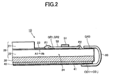
- Fig. 2 is a longitudinal section schematically showing the structure of the plasma display panel 10 and its wiring structure using TCP.
- the plasma display panel 10 has a display section main body 20 including a front glass substrate 21 and a rear glass substrate 22, a metal chassis 30 provided on the backside of the rear glass substrate 22, and a circuit board 40 provided on the backside of the metal chassis 30. Further, the plasma display panel 10 has a TCP 50 mounting a driver IC 51 and a thin sheet-like flat wiring cable 60 (hereinafter, referred to as "flat cable”) having a plurality of wiring patterns sandwiched between plastic films and having a predetermined flexibility, thereby realizing an external wiring between the display section main body 20 and the circuit board 40.
- the flat cable 60 for realizing the external wiring is FPC (Flexible Printed Circuit) having a certain flexibility or FFC (Flexible Flat Cable).
- the display section main body 20 comprises the front glass substrate 21 and the rear glass substrate 22, which are disposed to face each other with an electric discharge space (filled with a rare gas) interposed therebetween. Further, a plurality of row electrodes are formed with a predetermined pitch on the inner surface (facing the rear glass substrate 22) of the front glass substrate 21, while a plurality of column electrodes are formed (orthogonal to the row electrodes) with a predetermined pitch on the inner surface (facing the front glass substrate 21) of the rear glass substrate 22.
- each intersection of a row electrode with a column electrode forms an electric discharge cell, thereby forming a plurality of discharge cells by virtue of the respective row electrodes and column electrodes.
- the plurality of discharge cells can perform electric discharge and light emission can be effected corresponding to a driving electric power (for display) supplied to the respective electrodes from the driver C51, thereby displaying an image or the like.
- a plurality of wiring patterns A1 - Ak constituting a plurality of outgoing lines, power supply lines and earth lines connected to the respective column electrodes serving as display electrodes, are formed with a small wiring pitch on the outside edge 24 of the rear glass substrate 22, while connecting terminals CA1 - CAk are formed on the front end portions of the respective wiring patterns A1 - Ak.
- almost entire areas of the top surfaces of the wiring patterns A1 - Ak are covered by an insulating damp-proof film 23, with the connecting terminals CA1 - CAk constituting a first terminal group GR1.
- a second terminal group GR2 consisting of connecting terminals CB11 - CB1m and CB21 - CB2n are also formed on the outside edge 24 of the rear glass substrate 22, in positions adjacent to the first terminal group GR1.
- a third terminal group GR3 consisting of connecting terminals CC11 - CC1m and CC21 - CC2n is formed in a predetermined position more outward than the first and second terminal groups GR1 and GR2.
- a plurality of wiring patterns are connected corresponding to connecting terminals CB11 - CB1m and CB21 - CB2n of the second terminal group GR2, as well as connecting terminals CC11 - CC1m and CC21-CC2n of the third terminal group GR3.
- connecting terminal group formed on the substrate (i.e., film substrate) of TCP 50 are connecting terminal group provided on an end portion 52 (hereinafter, referred to as connecting end portion) of the substrate, and predetermined wiring patterns connected to the connecting terminal group and the driver IC 51. Then, the connecting terminal group is connected to the first and second terminal groups GR1 and GR2 by thermo-press bonding, while both ends of the TCP 50 are fixed to the outside edge 24 by damp-proof adhesive agents P1 and P2, thereby forming a desired wiring by virtue of the TCP 50.
- the predetermined connecting end portion 52 on one side of the TCP 50 serves as connecting portion for the above connecting terminal group.
- the connecting end portion 52 is connected to the first terminal group GR1 formed with the wiring patterns A1 - Ak, and also connected to the second terminal group GR2 connected with the third terminal group GR3, thereby forming a wiring connection between the first terminal group GR1 and the third terminal group GR3 through the TCP 50.
- an electrical circuit for performing display control or the like, and a plurality of wiring patterns 41, as well as connecting terminals CD1 - CDj are formed on the circuit board 40.
- These connecting terminals CD1 - CDj and third terminal group GR3 are connected to each other by the flat cable (FPC or FFC) 60.
- the first terminal group GR1 provided in the wiring patterns A1 - Ak and the second terminal group RG2 linked to the third terminal group GR3 are connected to each other through the TCP 50, while the third terminal group GR3 and the connecting terminals CD1 - CDj on the circuit board 40 side are connected to each other by the flat cable 60, thereby forming a desired wiring connection between the display section main body 20 and the circuit board 40.
- the driver IC 51 will supply, through the wiring patterns A1 - Ak, driving electric power (for display) corresponding to the display signals to the above-mentioned column electrodes in the display section main body 20.
- the display section main body 20 and the circuit board 40 are connected with common earth, while a predetermined power source voltage (for actuation) is supplied to the display section main body 20 from the circuit board 40.
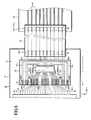
- Fig. 3 is a plan view showing wiring patterns and connecting terminals or the like formed on the side edge 24 of the rear glass substrate 22
- Fig. 4 is another plan view showing wiring patterns and connecting terminals or the like formed on the TCP 50
- Fig. 5 is a further plan view illustrating an expanded state of the wiring structure shown in Fig. 2.
- a plurality of wiring patterns A1 - Ak constituting a plurality of outgoing lines (linked to the respective column electrodes) , power supply lines, and earth lines are formed by vapor deposition with a small wiring pitch on the outside edge 24 of the rear glass substrate 22 of the plasma display panel 10.
- connecting terminals CA1 - CAk are arranged in one column along the direction Y orthogonal to an extending direction X of the wiring patterns A1 - Ak. Specifically, the connecting terminals CA1 - CAk and their adjacent areas are exposed without being covered by the insulating film 23 shown in Fig. 2. In this way, the first terminal group GR1 is formed by virtue of the connecting terminals CA1 - CAk.
- the wiring pattern A1 - Ak and the connecting terminals CA1 - CAk are used as power supply lines, while the wiring pattern Ak and the connecting terminal CAk are used as common earth lines, with the remaining wiring patterns A2 - Ak-1 and the remaining connecting terminals C2 - CAk -1 being connected to the column electrodes.
- connecting terminals CA1 - CAk serving as the first terminal group GR1 there are formed a plurality of connecting terminals CB11 - CB1m and CB21 - CB2n having an electric conductivity and constituting the second terminal group GR2, arranged in one column along the direction Y (in which the column electrodes are arranged).
- These connecting terminals CB11 - CB1m and CB21 - CB2n and their adjacent areas are exposed without being covered by the insulating film 23 shown in Fig. 2.
- a plurality of wiring patterns B11 - B1m and B21 - B2n having an electric conductivity and to be connected corresponding to the connecting terminals CB11 - CB1m and CB21 - CB2n of the second terminal group GR2 and also corresponding to the connecting terminals CC11 - CC1m and CB21 - CB2n of the third terminal group GR3, are formed by vapor deposition or the like, with the top surfaces of these wiring patterns B11 - B1m and B21 - B2n being covered by a damp-proof insulating film.
- the wiring pattern B1m is used as a power supply line and the wiring pattern B21 is used as a common earth line, with the remaining wiring patterns B11 - B1m-1 and B22 - B2n serving as signal input lines for inputting display signals supplied from the circuit board 40 through the flat cable 60.
- the TCP 50 has a length M extending from its predetermined connecting end portion 52 to the other end thereof, which is shorter than an interval L (shown in Fig. 3) between the first, second terminal groups GR1, GR2 and the third terminal group GR3. Therefore, when the TCP 50 is connected to the first and second terminal groups GR1 and GR2, the TCP will be received within the interval L.
- the connecting terminals CE1 - CEk, CF11 - CF1m, and CF21 - CF2n corresponding to the connecting terminals CA1 - CAk, CB11 - CB1m, and CB21 - CB2n of the first and second terminal groups GR1 and GR2 (shown in Fig. 3).
- the connecting terminals CE1 - CEk are formed with the same pitch as the connecting terminals CA1 - CAk of the first terminal group GR1, while the connecting terminals CF11 - CF1m and CF21 - CF2n are formed with the same pitch as the connecting terminals CB11 - CB1m and CB21 - CB2n of the second terminal group GR2. Furthermore, the positional relations among the connecting terminals CE1 - CEk, the connecting terminals CF11 - CF1m and CF21 - CF2n are set to be the same as the positional relation between the first terminal group GR1 and the second terminal group GR2.
- these connecting terminals CE1 - CEk, CF11 - CF1m, and CF21 - CF2n are formed of ametal having an electric conductivity, and exposed to both the front side and back side of the TCP 50 by virtue of a via-hole structure.
- the conductive wiring patterns E1 - Ek effecting wire connection between the connecting terminals CE1 - CEk and the respective output terminals of the driver IC 51 are formed, but also the conductive wiring patterns F11 - F1m and F21 - F2n effecting wire connection between the connecting terminals CF11 - CF1m, CF21 - CF2n and the respective output terminals of the driver IC 51 are formed, with the TCP 50 (except the connecting terminals CE1 - CEk, CF11 - CF1m, and CF21 - CF2n) being covered by the damp-proof insulating film or the like.
- the connecting terminals CF1, CF1m and the wiring patterns E1, F1m are used as power supply lines.
- the connecting terminals CEk, CF21 and the wiring patterns Ek, F21 are used as common earth lines.
- the connecting terminals CF11 - CF1m-1, CF22 - CF2n and the wiring patterns F11 - F1m-1 and F22 - F2n are used as signal input lines for inputting display signals to the driver IC 51.
- the connecting terminals CE2 - CEk-1 and the wiring patterns E2 - Ek-1 are used as output lines for transmitting the driving electric power (for display) outputted from the driver IC 51.
- the connecting terminals CA1 - CAk, CB11 - CB1m, and CB21 - CB2n of the first and second terminal groups GR1, GR2 are made coincident (in position) with the connecting terminals CE1 - CEk, CF11 - CF1m and CF21 - CF2n formed in the connection end portion 52 of the TCP50.
- the first and second terminal groups GR1, GR2 are connected mechanically and electrically to the connecting terminals CE1 - CEk, CF11 - CF1m, and CF21 - CF2n of the TCP 50 in only one step of operation. Subsequently, the TCP 50 is fixed to the rear glass substrate 22 side by means of damp-proof adhesive agents P1 and P2, as shown in Fig. 2.
- one connecting portion 61 of the flat cable 60 is connected to the connecting terminals CC1 - CC1m and CC21 - CC2n of the third terminal group GR3, while the other connecting portion 62 of the flat cable 60 is connected to the connecting terminals CD1 - CDj of the circuit board 40, all using an anisotropic conductive adhesive agent and by means of thermo-press bonding in only one step of operation, thereby realizing the wiring structure of the present invention.
- the TCP 50 is mounted on the outside edge 24 of the rear glass substrate 22, the length M of the TCP 50 can be shortened. Accordingly, as compared with the above-discussed prior art in which a long TCP is drawn around, the mounting structure has been greatly simplified and an internal space for receiving the mounting structure can be reduced, thereby making it possible to reduce production cost.
- the TCP 50 can be connected to the first and second terminal groups GR1, GR2 in only one step of operation (thermo-press bonding). Further, it is easy to set and adjust the positions of the connecting terminals CE1 - CEk, CF11 - CF1m, and CF21 - CF2n with respect to the first and second terminal groups GR1 and GR2. Meanwhile, it is also easy to change or repair an installed TCP 50.
- the rear glass substrate 22 and the circuit board 40 are connected to each other through the flat cable 60 such as cheap FPC and FFC or the like, it is allowed to reduce production cost. Further, as compared with the above-discussed prior art in which a long TCP is drawn around, the mounting structure has been greatly simplified and an internal space for receiving the mounting structure can be reduced.
- the length of the flat cable 60 can be easily set.
- the flat cable 60 can be freely laid out in an actual wiring process, thereby making it possible to improve a freedom in designing a mounting structure, as well as a freedom in an actual wiring process.
- a plasma display apparatus has long since been required to have its frame (for accommodating the display section main body 20 and the mounting structure) made in a thin thickness.
- the present embodiment provides a simplified wiring structure based on the TCP 50 and the flat cable 60, thus making it possible to reduce the thickness of the edge portion of the frame.
- FIGs. 2 - 5 describes a wiring structure formed by using one TCP 50 and one flat cable 60 corresponding to the TCP, it is also possible to use a plurality of TCPs and one flat cable corresponding to the TCPs, thereby forming a modified embodiment of the present invention.
- Fig. 6 is a plan view schematically showing another wiring structure as the modified embodiment of the present invention.
- elements identical with or corresponding to those in Figs. 2 - 5 will be represented by the same reference numerals.
- a plurality of wiring pattern groups Aa and Ab connected with and extending from a plurality of column electrodes are formed on the outside edge 24 of the rear glass substrate 22, with each of these wiring pattern groups Aa and Ab being connected with a first terminal group GR1 arranged in one column. Further, a plurality of second terminal groups GR2 arranged in one column are formed adjacent to the first terminal group GR1 of the wiring pattern group Aa and the first terminal group GR1 of the wiring pattern group Ab.
- a third terminal group GR3 is formed and collected in a position separated a predetermined distance from the first terminal groups GR1 and the second terminal groups GR2.
- the connecting terminals of the third terminal group GR3 are connected to the connecting terminals of the second terminal groups GR2 through wiring pattern groups Ba and Bb.
- an anisotropic conductive adhesive agent is used to perform a thermo-press bonding to connect (in one step of operation) the TCP 50a to the first terminal group GR1 and the second terminal groups GR2 relevant to the wiring pattern groups Aa and Ba.
- another TCP 50b is connected to the first terminal group GR1 and the second terminal group GR2 relevant to other wiring pattern groups Aa and Ba.
- connection terminal groups CEa and CFa corresponding to the first terminal group GR1 and the second terminal group GR2 are formed in an end portion on one side of TCP 50a equipped with an electronic device such as driver IC 51a.
- connection terminal groups CEb and CFb corresponding to the first terminal group GR1 and the second terminal group GR2 are formed on the TCP 50b equipped with an electronic device such as driver IC 51b.
- an anisotropic conductive adhesive agent is used to perform a thermo-press bonding so as to connect the terminal group including terminals CEa, CFa, CEb, CFb, and the first terminal group GR1 and second terminal groups GR2 (corresponding to the terminal group) in only one step of operation.
- the flat cable 60 such as FPC or FFC is connected between the third terminal group GR3 and the circuit board 40 by the thermo-press bondingusing the anisotropic conductive adhesive agent.
- the third terminal group GR3 for connecting the flat cable 60 can be collected in only one position, even when a plurality of TCPs 50a and 50b are to be attached, it is still possible to easily and quickly connect the third terminal group GR3 to the circuit board 40, thereby obtaining an improved efficiency for wiring process. Besides, it is allowed to reduce the number of parts required in the wiring structure.
- the wiring structure according to the present embodiment should not be limited to the above-described structure in which an electric power (for display) is supplied to the column electrodes formed in the display section main body of a plasma display apparatus, but can also be applied to various other wiring structures.
- wiring structure according to the present embodiment (including the modified embodiment) relates to a plasma display apparatus
- such wiring structure can also be applied to other flat panel type display apparatus such as a liquid crystal display or the like.
Landscapes
- Physics & Mathematics (AREA)
- Nonlinear Science (AREA)
- Mathematical Physics (AREA)
- Chemical & Material Sciences (AREA)
- Crystallography & Structural Chemistry (AREA)
- General Physics & Mathematics (AREA)
- Optics & Photonics (AREA)
- Devices For Indicating Variable Information By Combining Individual Elements (AREA)
- Liquid Crystal (AREA)
Applications Claiming Priority (2)
| Application Number | Priority Date | Filing Date | Title |
|---|---|---|---|
| JP2003058570 | 2003-03-05 | ||
| JP2003058570A JP2004271611A (ja) | 2003-03-05 | 2003-03-05 | フラットパネル型表示装置 |
Publications (2)
| Publication Number | Publication Date |
|---|---|
| EP1455377A2 true EP1455377A2 (fr) | 2004-09-08 |
| EP1455377A3 EP1455377A3 (fr) | 2007-09-05 |
Family
ID=32821204
Family Applications (1)
| Application Number | Title | Priority Date | Filing Date |
|---|---|---|---|
| EP04005125A Withdrawn EP1455377A3 (fr) | 2003-03-05 | 2004-03-04 | Dispositif d'affichage à panneau plat |
Country Status (3)
| Country | Link |
|---|---|
| US (1) | US7187427B2 (fr) |
| EP (1) | EP1455377A3 (fr) |
| JP (1) | JP2004271611A (fr) |
Cited By (3)
| Publication number | Priority date | Publication date | Assignee | Title |
|---|---|---|---|---|
| KR100797261B1 (ko) * | 2005-04-21 | 2008-01-23 | 후지츠 히다찌 플라즈마 디스플레이 리미티드 | 플라즈마 디스플레이 모듈 |
| EP1772889A3 (fr) * | 2005-10-06 | 2008-11-26 | LG Electronics Inc. | Appareil d'affichage à plasma |
| EP3333623A1 (fr) * | 2016-12-12 | 2018-06-13 | Lg Electronics Inc. | Afficheur |
Families Citing this family (22)
| Publication number | Priority date | Publication date | Assignee | Title |
|---|---|---|---|---|
| US7663607B2 (en) | 2004-05-06 | 2010-02-16 | Apple Inc. | Multipoint touchscreen |
| JP4290070B2 (ja) * | 2003-06-06 | 2009-07-01 | キヤノン株式会社 | 面状ケーブル部材の接続部の補強方法及び画像表示装置の製造方法 |
| US7843116B2 (en) * | 2005-01-14 | 2010-11-30 | Au Optronics Corporation | Plasma display panel thermal dissipation apparatus and method |
| KR20060094575A (ko) * | 2005-02-25 | 2006-08-30 | 신코엠 주식회사 | 칩 온 필름 패키지 |
| WO2007023517A1 (fr) * | 2005-08-22 | 2007-03-01 | Fujitsu Hitachi Plasma Display Limited | Câble plat et dispositif d'affichage à plasma |
| JP4635915B2 (ja) * | 2006-03-08 | 2011-02-23 | エプソンイメージングデバイス株式会社 | 電気光学装置及び電子機器 |
| JP2007316311A (ja) * | 2006-05-25 | 2007-12-06 | Funai Electric Co Ltd | 液晶テレビジョンおよびパネル型表示装置 |
| KR20110058895A (ko) | 2006-06-09 | 2011-06-01 | 애플 인크. | 터치 스크린 액정 디스플레이 |
| US20090066679A1 (en) * | 2006-07-04 | 2009-03-12 | Yoshikazu Kanazawa | Plasma display device |
| US9710095B2 (en) | 2007-01-05 | 2017-07-18 | Apple Inc. | Touch screen stack-ups |
| US8314785B2 (en) * | 2008-10-08 | 2012-11-20 | Samsung Sdi Co., Ltd. | Plasma display device |
| JP5452290B2 (ja) * | 2010-03-05 | 2014-03-26 | ラピスセミコンダクタ株式会社 | 表示パネル |
| US8804056B2 (en) | 2010-12-22 | 2014-08-12 | Apple Inc. | Integrated touch screens |
| US9235092B2 (en) * | 2012-03-21 | 2016-01-12 | Sharp Kabushiki Kaisha | Active matrix substrate and display panel including the same |
| WO2014164477A1 (fr) * | 2013-03-12 | 2014-10-09 | Apple Inc. | Baisse de la résistance de couche d'une couche conductrice |
| JP6369325B2 (ja) * | 2013-12-25 | 2018-08-08 | 三菱マテリアル株式会社 | パワーモジュール用基板、およびその製造方法、パワーモジュール |
| JP6318715B2 (ja) * | 2014-03-07 | 2018-05-09 | 富士通オプティカルコンポーネンツ株式会社 | 光モジュール |
| CN105161048B (zh) | 2015-10-27 | 2018-01-09 | 京东方科技集团股份有限公司 | 一种电路板和显示装置 |
| US10388213B2 (en) * | 2017-05-22 | 2019-08-20 | Microsoft Technology Licensing, Llc | Display and display integration method |
| CN110557887B (zh) * | 2018-05-31 | 2021-10-12 | 京东方科技集团股份有限公司 | 电路对位组件及显示装置 |
| KR102528670B1 (ko) | 2018-07-12 | 2023-05-04 | 엘지전자 주식회사 | 디스플레이 디바이스 |
| US20200119476A1 (en) * | 2018-10-16 | 2020-04-16 | HKC Corporation Limited | Display assembly and display device |
Citations (3)
| Publication number | Priority date | Publication date | Assignee | Title |
|---|---|---|---|---|
| EP0795772A1 (fr) * | 1996-03-15 | 1997-09-17 | Canon Kabushiki Kaisha | Structure de connection de circuit de commande et dispositif d'affichage comportant cette structure |
| US5838400A (en) * | 1994-10-21 | 1998-11-17 | Hitachi, Ltd. | Liquid crystal display device with reduced frame portion surrounding display area |
| US20010033355A1 (en) * | 2000-02-24 | 2001-10-25 | Takeshi Hagiwara | Mounting structure for semiconductor device, electro-optical device, and electronic apparatus |
Family Cites Families (3)
| Publication number | Priority date | Publication date | Assignee | Title |
|---|---|---|---|---|
| KR100304261B1 (ko) * | 1999-04-16 | 2001-09-26 | 윤종용 | 테이프 캐리어 패키지, 그를 포함한 액정표시패널 어셈블리,그를 채용한 액정표시장치 및 이들의 조립 방법 |
| JP4650822B2 (ja) | 2001-05-24 | 2011-03-16 | パナソニック株式会社 | フラットパネル型表示装置 |
| JP4059750B2 (ja) * | 2002-10-28 | 2008-03-12 | シャープ株式会社 | 電子モジュールおよびその製造方法 |
-
2003
- 2003-03-05 JP JP2003058570A patent/JP2004271611A/ja not_active Abandoned
-
2004
- 2004-02-13 US US10/777,142 patent/US7187427B2/en not_active Expired - Fee Related
- 2004-03-04 EP EP04005125A patent/EP1455377A3/fr not_active Withdrawn
Patent Citations (3)
| Publication number | Priority date | Publication date | Assignee | Title |
|---|---|---|---|---|
| US5838400A (en) * | 1994-10-21 | 1998-11-17 | Hitachi, Ltd. | Liquid crystal display device with reduced frame portion surrounding display area |
| EP0795772A1 (fr) * | 1996-03-15 | 1997-09-17 | Canon Kabushiki Kaisha | Structure de connection de circuit de commande et dispositif d'affichage comportant cette structure |
| US20010033355A1 (en) * | 2000-02-24 | 2001-10-25 | Takeshi Hagiwara | Mounting structure for semiconductor device, electro-optical device, and electronic apparatus |
Cited By (6)
| Publication number | Priority date | Publication date | Assignee | Title |
|---|---|---|---|---|
| KR100797261B1 (ko) * | 2005-04-21 | 2008-01-23 | 후지츠 히다찌 플라즈마 디스플레이 리미티드 | 플라즈마 디스플레이 모듈 |
| EP1772889A3 (fr) * | 2005-10-06 | 2008-11-26 | LG Electronics Inc. | Appareil d'affichage à plasma |
| US7573198B2 (en) | 2005-10-06 | 2009-08-11 | Lg Electronics Inc. | Plasma display apparatus |
| EP3333623A1 (fr) * | 2016-12-12 | 2018-06-13 | Lg Electronics Inc. | Afficheur |
| CN108230941A (zh) * | 2016-12-12 | 2018-06-29 | Lg电子株式会社 | 显示装置 |
| US10595426B2 (en) | 2016-12-12 | 2020-03-17 | Lg Electronics Inc. | Display device |
Also Published As
| Publication number | Publication date |
|---|---|
| US20040183484A1 (en) | 2004-09-23 |
| US7187427B2 (en) | 2007-03-06 |
| JP2004271611A (ja) | 2004-09-30 |
| EP1455377A3 (fr) | 2007-09-05 |
Similar Documents
| Publication | Publication Date | Title |
|---|---|---|
| EP1455377A2 (fr) | Dispositif d'affichage à panneau plat | |
| US6847415B1 (en) | Flat display unit and method fabricating same | |
| CN101807372B (zh) | 等离子体显示装置 | |
| US20030058230A1 (en) | Flat-panel type display apparatus | |
| US20050111175A1 (en) | Plasma display module | |
| EP2063691A2 (fr) | Dispositif à affichage plasma | |
| US7420821B2 (en) | Electronic module and driving circuit board therefor | |
| KR20030043647A (ko) | 플랙시블 기판의 실장방법 및 표시장치 | |
| US6052171A (en) | Liquid crystal display with electrically connected integrated circuits and opposite voltage line between input and output wirings | |
| US20050231495A1 (en) | Display device | |
| EP0735807A1 (fr) | Panneau à circuit électrique pour un dispositif d'affichage | |
| US8053988B2 (en) | Plasma display device | |
| US7285917B2 (en) | Connection member and driving device of plasma display panel | |
| US8011989B2 (en) | Method of making a plasma display panel with a novel connection structure | |
| JPH11305250A (ja) | 画像表示装置 | |
| US20070086149A1 (en) | Plasma display device | |
| JP3291423B2 (ja) | 表示パネルの実装方法および実装構造 | |
| JP3297084B2 (ja) | 表示装置及びそのフレキシブル基板 | |
| KR20090096107A (ko) | 플라즈마 디스플레이 장치 | |
| KR100599741B1 (ko) | 플라즈마 디스플레이 장치 | |
| KR100828875B1 (ko) | 면방전 교류 플라즈마 디스플레이 패널의 플랙시블 기판 | |
| KR100599771B1 (ko) | 테이프 캐리어 패키지의 배선구조 및 이 구조에 의해형성된 테이프 캐리어 패키지를 갖는 디스플레이 장치 | |
| KR100551030B1 (ko) | 화상 표시 장치 | |
| JP2004219719A (ja) | 表示装置 | |
| CN113077718A (zh) | 显示面板及显示装置 |
Legal Events
| Date | Code | Title | Description |
|---|---|---|---|
| PUAI | Public reference made under article 153(3) epc to a published international application that has entered the european phase |
Free format text: ORIGINAL CODE: 0009012 |
|
| AK | Designated contracting states |
Kind code of ref document: A2 Designated state(s): AT BE BG CH CY CZ DE DK EE ES FI FR GB GR HU IE IT LI LU MC NL PL PT RO SE SI SK TR |
|
| AX | Request for extension of the european patent |
Extension state: AL LT LV MK |
|
| PUAL | Search report despatched |
Free format text: ORIGINAL CODE: 0009013 |
|
| AK | Designated contracting states |
Kind code of ref document: A3 Designated state(s): AT BE BG CH CY CZ DE DK EE ES FI FR GB GR HU IE IT LI LU MC NL PL PT RO SE SI SK TR |
|
| AX | Request for extension of the european patent |
Extension state: AL LT LV MK |
|
| STAA | Information on the status of an ep patent application or granted ep patent |
Free format text: STATUS: THE APPLICATION HAS BEEN WITHDRAWN |
|
| 18W | Application withdrawn |
Effective date: 20070829 |