EP1451825B1 - Matrixadressierbares array integrierter transistor-/speicherstrukturen - Google Patents
Matrixadressierbares array integrierter transistor-/speicherstrukturen Download PDFInfo
- Publication number
- EP1451825B1 EP1451825B1 EP02804659A EP02804659A EP1451825B1 EP 1451825 B1 EP1451825 B1 EP 1451825B1 EP 02804659 A EP02804659 A EP 02804659A EP 02804659 A EP02804659 A EP 02804659A EP 1451825 B1 EP1451825 B1 EP 1451825B1
- Authority
- EP
- European Patent Office
- Prior art keywords
- transistor
- memory
- electrode
- electrodes
- source
- Prior art date
- Legal status (The legal status is an assumption and is not a legal conclusion. Google has not performed a legal analysis and makes no representation as to the accuracy of the status listed.)
- Expired - Lifetime
Links
Images

Classifications
-
- H—ELECTRICITY
- H01—ELECTRIC ELEMENTS
- H01L—SEMICONDUCTOR DEVICES NOT COVERED BY CLASS H10
- H01L21/00—Processes or apparatus adapted for the manufacture or treatment of semiconductor or solid state devices or of parts thereof
- H01L21/70—Manufacture or treatment of devices consisting of a plurality of solid state components formed in or on a common substrate or of parts thereof; Manufacture of integrated circuit devices or of parts thereof
- H01L21/77—Manufacture or treatment of devices consisting of a plurality of solid state components or integrated circuits formed in, or on, a common substrate
-
- H—ELECTRICITY
- H10—SEMICONDUCTOR DEVICES; ELECTRIC SOLID-STATE DEVICES NOT OTHERWISE PROVIDED FOR
- H10D—INORGANIC ELECTRIC SEMICONDUCTOR DEVICES
- H10D84/00—Integrated devices formed in or on semiconductor substrates that comprise only semiconducting layers, e.g. on Si wafers or on GaAs-on-Si wafers
- H10D84/80—Integrated devices formed in or on semiconductor substrates that comprise only semiconducting layers, e.g. on Si wafers or on GaAs-on-Si wafers characterised by the integration of at least one component covered by groups H10D12/00 or H10D30/00, e.g. integration of IGFETs
- H10D84/82—Integrated devices formed in or on semiconductor substrates that comprise only semiconducting layers, e.g. on Si wafers or on GaAs-on-Si wafers characterised by the integration of at least one component covered by groups H10D12/00 or H10D30/00, e.g. integration of IGFETs of only field-effect components
- H10D84/83—Integrated devices formed in or on semiconductor substrates that comprise only semiconducting layers, e.g. on Si wafers or on GaAs-on-Si wafers characterised by the integration of at least one component covered by groups H10D12/00 or H10D30/00, e.g. integration of IGFETs of only field-effect components of only insulated-gate FETs [IGFET]
- H10D84/85—Complementary IGFETs, e.g. CMOS
-
- H—ELECTRICITY
- H10—SEMICONDUCTOR DEVICES; ELECTRIC SOLID-STATE DEVICES NOT OTHERWISE PROVIDED FOR
- H10D—INORGANIC ELECTRIC SEMICONDUCTOR DEVICES
- H10D84/00—Integrated devices formed in or on semiconductor substrates that comprise only semiconducting layers, e.g. on Si wafers or on GaAs-on-Si wafers
- H10D84/01—Manufacture or treatment
- H10D84/0123—Integrating together multiple components covered by H10D12/00 or H10D30/00, e.g. integrating multiple IGBTs
- H10D84/0126—Integrating together multiple components covered by H10D12/00 or H10D30/00, e.g. integrating multiple IGBTs the components including insulated gates, e.g. IGFETs
- H10D84/0165—Integrating together multiple components covered by H10D12/00 or H10D30/00, e.g. integrating multiple IGBTs the components including insulated gates, e.g. IGFETs the components including complementary IGFETs, e.g. CMOS devices
- H10D84/0167—Manufacturing their channels
-
- H—ELECTRICITY
- H10—SEMICONDUCTOR DEVICES; ELECTRIC SOLID-STATE DEVICES NOT OTHERWISE PROVIDED FOR
- H10D—INORGANIC ELECTRIC SEMICONDUCTOR DEVICES
- H10D84/00—Integrated devices formed in or on semiconductor substrates that comprise only semiconducting layers, e.g. on Si wafers or on GaAs-on-Si wafers
- H10D84/01—Manufacture or treatment
- H10D84/0123—Integrating together multiple components covered by H10D12/00 or H10D30/00, e.g. integrating multiple IGBTs
- H10D84/0126—Integrating together multiple components covered by H10D12/00 or H10D30/00, e.g. integrating multiple IGBTs the components including insulated gates, e.g. IGFETs
- H10D84/0165—Integrating together multiple components covered by H10D12/00 or H10D30/00, e.g. integrating multiple IGBTs the components including insulated gates, e.g. IGFETs the components including complementary IGFETs, e.g. CMOS devices
- H10D84/0172—Manufacturing their gate conductors
-
- H—ELECTRICITY
- H10—SEMICONDUCTOR DEVICES; ELECTRIC SOLID-STATE DEVICES NOT OTHERWISE PROVIDED FOR
- H10D—INORGANIC ELECTRIC SEMICONDUCTOR DEVICES
- H10D84/00—Integrated devices formed in or on semiconductor substrates that comprise only semiconducting layers, e.g. on Si wafers or on GaAs-on-Si wafers
- H10D84/01—Manufacture or treatment
- H10D84/02—Manufacture or treatment characterised by using material-based technologies
- H10D84/03—Manufacture or treatment characterised by using material-based technologies using Group IV technology, e.g. silicon technology or silicon-carbide [SiC] technology
- H10D84/038—Manufacture or treatment characterised by using material-based technologies using Group IV technology, e.g. silicon technology or silicon-carbide [SiC] technology using silicon technology, e.g. SiGe
Definitions
- the present invention concerns a matrix-addressable array of integrated transistor/memory structures, as described in the preamble of claim 1.
- a matrix-addressable array is known from JP07106450.
- a major problem in modem computing is the physical split between storage devices and processing units, more specifically between CPUs and operating software, user software and user data.
- Recent improvements in effective CPU speeds e.g. the development from Pentium II onwards
- SRAM/EEPROM memory capacity inside the CPU
- the overall speed is still seriously hampered by the fact that most software and data still uses the hard disk as primary storage medium.
- the transfer rate of hard disks has improved in recent years, as have the capacity of buses, the maximum speed potential is still controlled by the very slow access speed of the hard disks, a speed which barely has improved the last 10-15 years, and which will not improve substantially either as long as this primary storage medium remains a mechanically operated device.
- a major object of the present invention is to obviate or eliminate the above problems by introducing a novel architecture allowing the integration of non-volatile memory and high-speed transistor circuitry which can be applied to inorganic as well as organic electronics or hybrids thereof, and which moreover is not limited to planar devices, but equally well applicable to volumetric devices.
- the transistor/memory structure comprises a third electrode layer of semiconducting material opposite the source and drain electrode layer, said third electrode layer comprising a second gate electrode extending in the same direction as the first gate electrode and registering therewith, whereby the transistor/memory structure is realized as a dual gate field-effect transistor.
- the first memory cell contacts the source and the gate electrodes
- the second memory cell contacts the drain and the gate electrodes
- the third memory cell contacts the source and the drain electrodes.
- the memory material in the third memory cell preferable has a thickness different from that of the first and second memory cells, and in that case the memory material preferably is a ferroelectric or electret organic material, preferably a polymer or copolymer.
- the semiconducting material advantageously is an inorganic semiconducting material, preferably amorphous silicon, polycrystalline silicon or microcrystalline silicon; or the semiconducting material is advantageously an organic semiconducting material, preferably a semiconducting polymer or pentacene.
- an additional transistor memory is provided in registration with the first single transistor/memory structure opposite the gate electrode thereof and inverted in relation to the first single transistor memory structure, said additional transistor/memory structure sharing the same gate electrode with the latter, thus realizing a dual transistor/memory structure with common gate and six memory cells, and then the dual transistor/memory structure preferably realizes a common gate complementary field-effect transistor.
- the dual transistor memory structure advantageously is provided with at least one additional gate electrode, said at least one additional gate electrode being provided on one of the layers of strigducting material opposite the source/drain electrode layer.
- the matrix-addressable array is realized as a three-dimensional array by stacking two or more two-dimensional arrays of transistor/memory structures, and that a two-dimensional array is isolated from an adjacent neighbouring two-dimensional array by a separation layer, and then the separation layer preferably is selected as one of the following, viz. a layer of insulating material, a layer of conducting or semiconducting material coated to form an insulating barrier, or a layer of conducting or semiconducting material surface-oxidized to form the insulating barrier.
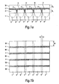
- a dense electrode arrangement as described therein corresponds to the electrode arrangements shown in cross section in fig. 1a and plan view in fig. 1b, in casu the arrangement of the electrodes in the electrode layers E 1 and E 2 as indicated in fig. 1a.
- a pitch deriving from constraints imposed by design rules of conventional patterning technology, e.g. photomicrolithography separate patterning and molding processes are used to form electrode sets E 1 ; E 2 with e.g.
- the dense electrode arrangement as disclosed in the above-mentioned international patent application allows the realization of dense matrices of cells of functional material provided say between electrode sets such as E 1 and E 2 and addressable thereby.
- fig. 1a can be taken to render a cross section of transistor structures arranged in a matrix, as readily can be seen from the plan view in fig. 1b.
- a source electrode 2 is formed in the first electrode layer E 1 running parallel to drain electrode 6 of about similar dimensions.
- Source and drain electrodes 2;6 are provided on a semiconducting substrate 1 e.g.
- the source and drain electrodes are as before isolated by barrier material 4 filling the recesses 3 therebetween and covering the top surfaces thereof, thus providing an insulating layer 4.
- the crosswise oriented gate electrodes 10 of the field-effect transistor structures are provided as seen to advantage in the plan view in fig. 1b.
- the channel length L of the transistor channel 8 can be made almost arbitrarily small, conforming to the thickness of a layer 4 which by methods well-known to persons skilled in the art can be deposited with thickness down to almost monoatomic size.
- the channel width W will be given by the width of the gate electrodes 10 and hence the ratio W/L can be made very large, thus giving a very high drain current I D as desirable.
- Present-day technology for patterning in the region well beyond the 0,1 ⁇ m range will hence allow transistor matrices as shown in e.g. fig. 1b and with transistor structures realized in a corresponding small scale.
- a single transistor/memory structure T 1 according to the present invention is shown in fig. 2a and appears structurally similar to corresponding structures in e.g. fig. 1a.
- a source electrode 2 and a drain electrode 6 are provided on a substrate or layer 1 of semiconducting material which has suitably been doped to form a source region 9, an ultrashort transistor channel 8 and a drain region 5 in the semiconducting substrate.
- a barrier of insulating material 4 as shown in fig.
- this material is replaced by a memory material in the form of a thin layer 11 of a polarizable dielectric material capable of exhibiting hysteresis, particularly a ferroelectric or electret material.
- the ferroelectric memory material as known to persons skilled in the art be a ferroelectric polymer or copolymer and then in the latter case most preferably a polyvinylidene fluoride/tri-fluoroethylene copolymer (PVDF-TrFE) which can be deposited in extremely thin layers, e.g. down to a nanometer scale, and which of course, being a ferroelectric material, also can provide the necessary insulating properties.
- the memory material 11 is provided as shown in fig.
- the transistor/memory structure T 1 is thus now also combined with the memory material 11 to form three separate memory cells which better can be seen in fig. 2c, which in perspective shows a layer of memory material 11 with all other features removed.
- This memory material 11 now has three distinct portions, viz. first portion 11a forming a first memory cell which can be addressed via the gate electrode 10 and the source electrode 2, a second portion 11b forming a second memory which can be addressed via the gate electrode 10 and the drain electrode 6, and a third portion 11c forming a third memory cell in the recess 3 between the source and drain electrodes 2;6 and addressable thereby.
- three memory cells 11a, 11b, 11c can be addressed, i.e. read and written independently of the operation of the field-effect transistor proper.
- three memory cells can store a three bit word, i.e. for instance any of the binary words 000, 001, 010, 011, 100, 101 and 111. Write/read of such three bit binary words will of course be a matter of protocol, as well-known to persons skilled in the art, and shall not be further discussed herein. The whole operation of the device shall be explained more fully in the following section.
- the memory material 11 forming the three memory cells 11a, 11b, 11c as shown in fig. 2c allows multidirectional switching as shall now be explained.
- the first cell 11a corresponds to the portion of memory material 11 between the source electrode 2 and the gate electrode 10 and will be switched in a direction orthogonal to the surfaces of these electrodes and the memory cell by applying a voltage to the source electrode 2 and the gate electrode 10, creating a potential therebetween and an electric field across the memory cell 11 a, which now as an e.g. ferroelectric memory material can be polarized in either the up and down direction and thus allowing the storage of a binary digit.
- ferroelectric memory material can be polarized in either the up and down direction and thus allowing the storage of a binary digit.
- the same consideration applies to the memory cell 11b in the portion of the memory material 11 between the drain electrode 6 and the gate electrode 10.
- a third memory cell 11c is provided by the memory material 11 in the recess 3 between the source electrode 2 and the drain electrode 6 and will be similarly switched by applying voltage between these, setting up an electric field across the memory cell 11c therebetween.
- a typical preferred ferroelectric material such as polyvinylidene trifluoride-trifluoroethylene (PVDF-TrFE)
- PVDF-TrFE polyvinylidene trifluoride-trifluoroethylene
- the field strength required is in other words related to the thickness of the thin-film memory material 11, and the thickness thereof in the memory cells 11a and 11b can be different from that in the memory cell 11c.
- memory cell 11a can now be denoted source/gate memory cell (S/G memory cell) and similarly memory cell 11b the drain/gate memory cell (D/G memory cell), while then of course memory cell 11c can be denoted the source/drain memory cell (S/D memory cell).
- S/G and D/G memory cell material 11 have the same thickness, these two cells will be switched by the same applied field strength, while the memory material in the S/D memory cell can be thicker or thinner than in the two former memory cells, and hence shall allow switching at a different field strength between the source and drain electrodes 2;6.
- the transistor structure formed by the source and drain electrodes 2;6 the doped regions 5,8,9 and the gate electrodes 10 shall allow the transistor switching independently of the memory switching and this implies that the transistor shall be switched by allowing a lower source or drain voltage than that required to switch the S/D memory cell and a gate electrode voltage much lower than that required for switching either the S/G memory cell or the D/G memory cell. In practice, the switching of these latter two memory cells will be completely independent of the transistor switching.
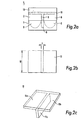
- Fig. 3a shows a first preferred embodiment wherein a second transistor/memory structure is provided above a first single transistor/memory structure T 1 .
- the two transistor/memory structures T 1 , T 2 shares the same gate electrode 10, while the electrode layers comprising the source/drain electrodes 2;6 are provided inverted respective to each other on opposite sides of the common gate electrode 10.
- the doped regions of the transistors are as before found in the semiconducting substrate 1 provided on either side in each of the transistor/memory structures T 1 ;T 2 as shown.
- These combined structures actually are a common gate transistor structure and could appropriately connected be used to realize a common gate complementary transistor circuit where T 1 forms the first transistor of the circuit and T 2 the second transistor of the circuit.
- the substrates 1 must be doped accordingly to form respectively a npn or a pnp channel structure.
- a similar dual transistor/memory structure is shown in fig. 3b, but now with the positions of the source and drain electrodes 2;6 reversed in their respective transistor/memory structures T 1 ;T 2 .
- the dual transistor/memory structures in fig. 3a and 3b are realized with six memory cells that can be separately addressed. It will also be evident that the structures depicted in figs. 3a and 3b shall allow six independently switchable memory cells and thus the possibility of storing a six bit binary word and writing and reading the same with any suitable protocol as obvious to persons skilled in the art.
- a second embodiment of the dual transistor/memory structure is shown in fig. 3c, wherein the second transistor/memory structure T 2 is provided with a second gate electrode 10, thus making T 2 a dual gate transistor/memory structure.
- a third embodiment of dual transistor/memory structure is shown in fig. 3d and is similar to the embodiment in fig. 3c, but now also with a second gate electrode 10' added to the transistor/memory structure T 1 , thus making both structures T 1 ;T 2 dual gate transistor/memory structures with gate electrodes 10, 10'.
- the substrate i.e. the layer of semiconducting material 1 can preferably be made of silicon; in case either amorphous, polycrystalline or microcrystalline silicon.
- an inorganic semiconductor material such as silicon is of course the possibility of forming barrier layer thereupon by performing a surface oxidation thereof.
- the layer of semiconductor material being an organic semiconductor, e.g. a semiconducting polymer or a cyclic compound such as pentacene, as well-known to persons skilled in the art.
- Laying down the electrodes of the electrode layer E 1 on an organic semiconducting material one must then, take precautions to heed the compatibility between the electrodes materials and any organic semiconducting material with regard to process temperature regime and so on.
- the memory material 11 shall be a dielectric and polarizable material with ferroelectric or electret properties that is capable of showing hysteresis when subjected to an electrical field. Most preferably such materials will be organic as mentioned, polymers or copolymers and even more preferably FVDF-TrFE will be used as memory material.
- An added advantage of such memory materials is that their dielectric properties allow their function as electrically insulating barrier materials as well, and further advantage is the possibility of applying them in global layers of extreme thinness down to few nanometres and finally that they can easily be applied on complex surface geometries to form memory cells, including complete filling of the recesses 3 such as formed between the source and drain electrodes 2;6.
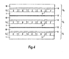
- the matrix-addressable array of transistor/memory structures have been more or less treated as a kind of two-dimensional array, but it is also possible to stack such two-dimensional arrays to form three-dimensional arrays, as shown in fig. 4, which renders a three-dimensional matrix-addressable array according to the invention and formed by three stacked two-dimensional arrays S 1 , S 2 , S 3 .
- the point of departure here is of course, the single transistor/memory structure in fig. 1a, but a three-dimensional matrix-addressable arrays of such transistor memory structures need not be limited to that particular one, but could rely on the dual structures for instance shown in fig.
- This separation layer could be a separate material and for the sake of that consist of a dielectric memory material 11, but could also be a barrier coating with insulating properties applied to the gate electrodes 10.
- this layer of semiconducting material could be treated to form a barrier layer at its surface adjacent to the gate electrode, e.g. by ensuring that a surface of an inorganic semiconducting material used in layer 1 e.g. is oxidized before it is located upon the underlying stack. This is of course easy to achieve when the inorganic semiconducting material as silicon, by simply performing a surface oxidation thereof.
- the present invention provides a matrix-addressable array of integrated transistor/memory structure in two or three dimensions with the integration of memory cells with transistor switches and allowing the switching of either to take place in separate voltage regimes, without a switching of e.g. a memory cell affecting the transistor integrated therewith.
- Information to be processed or for device operation can be stored in memory cells integrated in the transistor circuitry and hence eliminate the need for external access and peripheral storage devices.
- any two-dimensional array it will be possible to separate groups of transistor/memory structures and form circuit arrangements thereof as desired, e.g. by removing these transistor memory structures in certain portions of the two-dimensional array and then providing appropriate vias and interconnects with necessary insulation and barrier layers as required to form, say logic cells and arithmetic registers with integrated memory in a combined processor/memory circuit which moreover also can be realized in three dimensions allowing a higher degree of connectivity.
Landscapes
- Engineering & Computer Science (AREA)
- Microelectronics & Electronic Packaging (AREA)
- Condensed Matter Physics & Semiconductors (AREA)
- General Physics & Mathematics (AREA)
- Manufacturing & Machinery (AREA)
- Computer Hardware Design (AREA)
- Physics & Mathematics (AREA)
- Power Engineering (AREA)
- Semiconductor Memories (AREA)
- Non-Volatile Memory (AREA)
- Thin Film Transistor (AREA)
- Dram (AREA)
- Metal-Oxide And Bipolar Metal-Oxide Semiconductor Integrated Circuits (AREA)
Claims (14)
- Matrix-adressierbares Array von integrierten Transistor-/Speicherstrukturen,
wobei das Array mindestens eine Schicht (1) aus Halbleitermaterial, mindestens eine erste Elektrodenschicht (E1) und eine zweite Elektrodenschicht (E2), die Elektroden (2, 6, 10) besitzen, sowie ein Speichermaterial (11) aufweist, das mit den Elektroden (2, 6, 10) in Kontakt steht,
wobei das Speichermaterial (11) ein polarisierbares dielektrisches Material ist, das Hysterese zeigen kann, insbesondere ein ferroelektrisches Material oder Elektret-Material,
wobei die zweite Elektrodenschicht (E2) sich oberhalb der ersten Elektrodenschicht (E1) befindet, die sich oberhalb der Schicht (1) aus Halbleitermaterial befindet,
wobei die Elektroden (2, 6, 10) in den ersten und zweiten Elektrodenschichten (E1; E2) in jeder Schicht als kontinuierliche oder unterbrochene parallel verlaufende Strukturen vorgesehen sind,
wobei die mindestens eine Schicht (1) aus Halbleitermaterial und die ersten und zweiten Elektrodenschichten (E1; E2) Feldeffekttransistor-Strukturen bilden,
wobei die Elektroden (2, 6) der ersten Elektrodenschicht (E1) Source/Drain-Elektrodenpaare der Feldeffekttransistor-Strukturen bilden,
wobei die Elektroden der zweiten Elektrodenschicht (E2) die Gateelektroden (10) der Feldeffekttransistor-Strukturen bilden, wobei die Gateelektroden in jedem Falle in einer im wesentlichen orthogonalen Orientierung relativ zu den Elektroden (2, 6) der ersten Elektrodenschicht (E1) vorgesehen sind,
dadurch gekennzeichnet,
daß die Source- und Drainelektroden (2; 6) einer einzelnen Transistor-/Speicherstruktur (T1) mit einer schmalen vertikalen Aussparung (3) getrennt sind, die sich dazwischen und hinunter zu der Schicht (1) aus Halbleitermaterial erstreckt,
daß ein Transistorkanal (8) in der Halbleiterschicht (1) unterhalb der Aussparung (3) zwischen den Source- und Drainelektroden (2; 6) vorgesehen ist, daß die Source- und Drainbereiche (9; 5) der Transistorstrukturen unterhalb der Source- und Drainelektroden (2; 6) zu beiden Seiten des Transistorkanals (8) vorgesehen sind,
daß das Speichermaterial (11) die Aussparung (3) zwischen den Source- und Drainelektroden (2; 6) ausfüllend vorgesehen ist und einen Raum zwischen der Gateelektrode (10) und der Drainelektrode (6) sowie zwischen der Gateelektrode (10) und der Sourceelektrode (2) ausfüllt, so daß das Speichermaterial (11) mit der Gateelektrode (10), der Sourceelektrode (2) und der Drainelektrode (6) in Kontakt steht,
so daß der Transistorkanal (8) mit einer Länge L, die der Breite der Aussparung (3) entspricht, und einer Breite W ausgebildet ist, die der Breite der Gateelektrode (10) entspricht, wobei L ein Bruchteil von W ist,
und daß drei Speicherzellen (11a, 11b, 11c) in dem Speichermaterial (11) jeweils zwischen der Sourceelektrode (2) und der Gateelektrode (10), zwischen der Drainelektrode (6) und der Gateelektrode (10) sowie in der Aussparung zwischen den Source- und Drainelektroden (2; 6) ausgebildet sind. - Matrix-adressierbares Array nach Anspruch 1,
dadurch gekennzeichnet,
daß eine Transistor-/Speicherstruktur (T1) eine dritte Elektrodenschicht (10') aus Halbleitermaterial, der Source- und Drainelektrodenschicht (E1) gegenüberliegend aufweist, wobei die dritte Elektrodenschicht (10') eine zweite Gateelektrode aufweist, die sich in der gleichen Richtung wie die erste Gateelektrode (10) erstreckt und mit dieser zusammenpaßt, so daß die Transistor-/Speicherstruktur als Feldeffekttransistor mit zwei Gates realisiert ist. - Matrix-adressierbares Array nach Anspruch 1,
dadurch gekennzeichnet,
daß die erste Speicherzelle (11a) mit den Source- und Gateelektroden (2; 10) in Kontakt steht. - Matrix-adressierbares Array nach Anspruch 1,
dadurch gekennzeichnet,
daß die zweite Speicherzelle (11b) mit den Drain- und Gateelektroden (6; 10) in Kontakt steht. - Matrix-adressierbares Array nach Anspruch 1,
dadurch gekennzeichnet,
daß die dritte Speicherzelle (11c) mit den Source- und Drainelektroden (2; 6) in Kontakt steht. - Matrix-adressierbares Array nach Anspruch 5,
dadurch gekennzeichnet,
daß das Speichermaterial (11) in der dritten Speicherzelle (11c) eine Dicke besitzt, die sich von der der ersten und zweiten Speicherzellen (11a ; 11b) unterscheidet. - Matrix-adressierbares Array nach Anspruch 5,
dadurch gekennzeichnet,
daß das Speichermaterial (11) ein ferroelektrisches oder organisches Elektret-Material ist, vorzugsweise ein Polymer oder Copolymer. - Matrix-adressierbares Array nach Anspruch 1,
dadurch gekennzeichnet,
daß das Halbleitermaterial ein anorganisches Halbleitermaterial ist, vorzugsweise amorphes Silizium, polykristallines Silizium oder mikrokristallines Silizium. - Matrix-adressierbares Array nach Anspruch 1,
dadurch gekennzeichnet,
daß das Halbleitermaterial ein organisches Halbleitermaterial ist, vorzugsweise ein halbleitendes Polymer oder Pentacen. - Matrix-adressierbares Array nach Anspruch 1,
dadurch gekennzeichnet,
daß eine zusätzliche Transistor-/Speicherstruktur (T2) in Übereinstimmung mit der ersten einzelnen Transistor-/Speicherstruktur (T1) vorgesehen ist, und zwar ihrer Gateelektrode (10) gegenüberliegend und umgekehrt in Relation zu der ersten einzelnen Transistor-/Speicherstruktur, wobei die zusätzliche Transistor-/Speicherstruktur (T2) dieselbe Gateelektrode (10) mit der letzteren Struktur (T1) teilt, so daß eine doppelte Transistor-/Speicherstruktur mit gemeinsamem Gate und sechs Speicherzellen realisiert ist. - Matrix-adressierbares Array nach Anspruch 10,
dadurch gekennzeichnet,
daß die doppelte Transistor-/Speicherstruktur einen komplementären Feldeffekttransistor mit gemeinsamem Gate bildet. - Matrix-adressierbares Array nach Anspruch 10,
dadurch gekennzeichnet,
daß die doppelte Transistor-/Speicherstruktur mit mindestens einer zusätzlichen Gateelektrode (10') versehen ist, wobei die mindestens eine zusätzliche Gateelektrode auf einer der Schichten (1) aus Halbleitermaterial gegenüber der Source/Drain-Elektrodenschicht vorgesehen ist. - Matrix-adressierbares Array nach Anspruch 1,
dadurch gekennzeichnet,
daß das Matrix-adressierbare Array als dreidimensionales Array ausgebildet ist, in dem zwei oder mehr zweidimensionale Arrays (5) aus Transistor-/Speicherstrukturen aufeinandergestapelt sind,
und daß ein zweidimensionales Array von einem angrenzenden benachbarten zweidimensionalen Array mit einer Trennschicht (12) getrennt ist. - Matrix-adressierbares Array nach Anspruch 13,
dadurch gekennzeichnet,
daß die Trennschicht (12) als eine aus den folgenden Schichten gewählt ist, nämlich einer Schicht aus Isoliermaterial, einer Schicht aus leitendem oder halbleitendem Material, das zur Bildung einer isolierenden Barriere beschichtet ist, oder einer Schicht aus leitendem oder halbleitendem Material, dessen Oberfläche oxidiert ist, um die isolierende Barriere zu bilden.
Applications Claiming Priority (3)
| Application Number | Priority Date | Filing Date | Title |
|---|---|---|---|
| NO20016041A NO20016041A (no) | 2001-12-10 | 2001-12-10 | Matriseadresserbar gruppe av integrerte transistor/minnestrukturer |
| NO20016041 | 2001-12-10 | ||
| PCT/NO2002/000426 WO2003050814A1 (en) | 2001-12-10 | 2002-11-18 | A matrix-addressable array of integrated transistor/memory structures |
Publications (2)
| Publication Number | Publication Date |
|---|---|
| EP1451825A1 EP1451825A1 (de) | 2004-09-01 |
| EP1451825B1 true EP1451825B1 (de) | 2007-03-14 |
Family
ID=19913138
Family Applications (1)
| Application Number | Title | Priority Date | Filing Date |
|---|---|---|---|
| EP02804659A Expired - Lifetime EP1451825B1 (de) | 2001-12-10 | 2002-11-18 | Matrixadressierbares array integrierter transistor-/speicherstrukturen |
Country Status (11)
| Country | Link |
|---|---|
| EP (1) | EP1451825B1 (de) |
| JP (1) | JP2005512338A (de) |
| KR (1) | KR100556089B1 (de) |
| CN (1) | CN1602531A (de) |
| AT (1) | ATE357045T1 (de) |
| AU (1) | AU2002366675A1 (de) |
| CA (1) | CA2466153C (de) |
| DE (1) | DE60218887D1 (de) |
| NO (1) | NO20016041A (de) |
| RU (1) | RU2287205C2 (de) |
| WO (1) | WO2003050814A1 (de) |
Families Citing this family (6)
| Publication number | Priority date | Publication date | Assignee | Title |
|---|---|---|---|---|
| US8120082B2 (en) | 2005-09-12 | 2012-02-21 | University of Seoul, Foundation of Industry-Academic Cooperation | Ferroelectric memory device and method for manufacturing the same |
| KR100988227B1 (ko) * | 2005-09-12 | 2010-10-18 | 서울시립대학교 산학협력단 | 강유전체 메모리장치 및 그 제조방법 |
| EP1808863A1 (de) * | 2006-01-16 | 2007-07-18 | Deutsche Thomson-Brandt Gmbh | Verfahren und Vorrichtung zur Aufzeichnung von Hochgeschwindigkeitseingabedaten auf einer Speichergerätematrix |
| KR101245293B1 (ko) * | 2006-01-19 | 2013-03-19 | 서울시립대학교 산학협력단 | 강유전체 메모리의 제조를 위한 강유전 물질 |
| US10163917B2 (en) * | 2016-11-01 | 2018-12-25 | Micron Technology, Inc. | Cell disturb prevention using a leaker device to reduce excess charge from an electronic device |
| CN112908368B (zh) * | 2021-02-04 | 2023-03-21 | 清华大学 | 基于单片三维异质集成的三态内容寻址存储器 |
Family Cites Families (6)
| Publication number | Priority date | Publication date | Assignee | Title |
|---|---|---|---|---|
| US4952031A (en) * | 1987-06-19 | 1990-08-28 | Victor Company Of Japan, Ltd. | Liquid crystal display device |
| RU2054753C1 (ru) * | 1993-03-19 | 1996-02-20 | Институт физики полупроводников СО РАН | Устройство считывания на приборах с зарядовой связью для двумерных приемников изображения |
| JPH07106450A (ja) * | 1993-10-08 | 1995-04-21 | Olympus Optical Co Ltd | 強誘電体ゲートトランジスタメモリ |
| DE69739045D1 (de) * | 1997-08-27 | 2008-11-27 | St Microelectronics Srl | Herstellungsverfahren für elektronische Speicherbauelemente mit virtueller Masse |
| US6072716A (en) * | 1999-04-14 | 2000-06-06 | Massachusetts Institute Of Technology | Memory structures and methods of making same |
| US6473388B1 (en) * | 2000-08-31 | 2002-10-29 | Hewlett Packard Company | Ultra-high density information storage device based on modulated cathodoconductivity |
-
2001
- 2001-12-10 NO NO20016041A patent/NO20016041A/no unknown
-
2002
- 2002-11-18 JP JP2003551784A patent/JP2005512338A/ja not_active Abandoned
- 2002-11-18 AT AT02804659T patent/ATE357045T1/de not_active IP Right Cessation
- 2002-11-18 CN CNA028245377A patent/CN1602531A/zh active Pending
- 2002-11-18 RU RU2004120776/28A patent/RU2287205C2/ru not_active IP Right Cessation
- 2002-11-18 WO PCT/NO2002/000426 patent/WO2003050814A1/en not_active Ceased
- 2002-11-18 DE DE60218887T patent/DE60218887D1/de not_active Expired - Lifetime
- 2002-11-18 CA CA002466153A patent/CA2466153C/en not_active Expired - Fee Related
- 2002-11-18 AU AU2002366675A patent/AU2002366675A1/en not_active Abandoned
- 2002-11-18 EP EP02804659A patent/EP1451825B1/de not_active Expired - Lifetime
- 2002-11-18 KR KR1020047008856A patent/KR100556089B1/ko not_active Expired - Fee Related
Also Published As
| Publication number | Publication date |
|---|---|
| WO2003050814A1 (en) | 2003-06-19 |
| EP1451825A1 (de) | 2004-09-01 |
| KR100556089B1 (ko) | 2006-03-03 |
| JP2005512338A (ja) | 2005-04-28 |
| CN1602531A (zh) | 2005-03-30 |
| CA2466153A1 (en) | 2003-06-19 |
| AU2002366675A1 (en) | 2003-06-23 |
| NO20016041D0 (no) | 2001-12-10 |
| CA2466153C (en) | 2007-01-23 |
| ATE357045T1 (de) | 2007-04-15 |
| KR20040064733A (ko) | 2004-07-19 |
| NO314736B1 (no) | 2003-05-12 |
| DE60218887D1 (de) | 2007-04-26 |
| RU2287205C2 (ru) | 2006-11-10 |
| NO20016041A (no) | 2003-05-12 |
| RU2004120776A (ru) | 2005-09-20 |
Similar Documents
| Publication | Publication Date | Title |
|---|---|---|
| US6724028B2 (en) | Matrix-addressable array of integrated transistor/memory structures | |
| KR100392446B1 (ko) | 스케일가능 집적 데이터 처리 디바이스 | |
| US7613027B2 (en) | Semiconductor memory device with dual storage node and fabricating and operating methods thereof | |
| US20230077181A1 (en) | Three-dimensional nor memory string arrays of thin-film ferroelectric transistors | |
| US20250308569A1 (en) | Hybrid memory device and method of forming the same | |
| CN111312747B (zh) | 一种阻变存储器单元及制备方法 | |
| US10636802B2 (en) | Two-terminal non-volatile memristor and memory | |
| JPH10506237A (ja) | 固定記憶装置及びその製造方法 | |
| WO2000070683A1 (en) | Semiconductor memory | |
| JP3825257B2 (ja) | 容量増大化可能なデータ処理装置 | |
| EP1451825B1 (de) | Matrixadressierbares array integrierter transistor-/speicherstrukturen | |
| KR20240012750A (ko) | 비휘발성 메모리 장치 | |
| CN115497532A (zh) | 存储器结构及其制造与控制方法 | |
| US20240347109A1 (en) | Memory array of three-dimensional nor memory strings with word line select device | |
| US6730930B2 (en) | Memory element and method for fabricating a memory element | |
| EP1488427B1 (de) | Volumetrische datenspeichervorrichtung mit mehreren gestapelten matrixadressierbaren speichereinrichtungen | |
| US20090242955A1 (en) | Integrated Circuit, Memory Device and Methods of Manufacturing the Same | |
| CN114639773A (zh) | 一种半导体结构、存储单元及存储阵列 | |
| HK1075323A (en) | A matrix-addressable array of integrated transistor/memory structures | |
| US20240334714A1 (en) | Method of manufacturing semiconductor device using isolation structure | |
| CN120659328A (zh) | 一种存储阵列、其制作方法、存储器及电子设备 | |
| CN118510289A (zh) | 一种功能单元及其数据操作方法、堆叠结构 | |
| KR19990008826A (ko) | 반도체 메모리 | |
| KR20090054685A (ko) | 비휘발성 메모리 장치 |
Legal Events
| Date | Code | Title | Description |
|---|---|---|---|
| PUAI | Public reference made under article 153(3) epc to a published international application that has entered the european phase |
Free format text: ORIGINAL CODE: 0009012 |
|
| 17P | Request for examination filed |
Effective date: 20040507 |
|
| AK | Designated contracting states |
Kind code of ref document: A1 Designated state(s): AT BE BG CH CY CZ DE DK EE ES FI FR GB GR IE IT LI LU MC NL PT SE SK TR |
|
| GRAP | Despatch of communication of intention to grant a patent |
Free format text: ORIGINAL CODE: EPIDOSNIGR1 |
|
| GRAS | Grant fee paid |
Free format text: ORIGINAL CODE: EPIDOSNIGR3 |
|
| GRAA | (expected) grant |
Free format text: ORIGINAL CODE: 0009210 |
|
| AK | Designated contracting states |
Kind code of ref document: B1 Designated state(s): AT BE BG CH CY CZ DE DK EE ES FI FR GB GR IE IT LI LU MC NL PT SE SK TR |
|
| PG25 | Lapsed in a contracting state [announced via postgrant information from national office to epo] |
Ref country code: NL Free format text: LAPSE BECAUSE OF FAILURE TO SUBMIT A TRANSLATION OF THE DESCRIPTION OR TO PAY THE FEE WITHIN THE PRESCRIBED TIME-LIMIT Effective date: 20070314 Ref country code: AT Free format text: LAPSE BECAUSE OF FAILURE TO SUBMIT A TRANSLATION OF THE DESCRIPTION OR TO PAY THE FEE WITHIN THE PRESCRIBED TIME-LIMIT Effective date: 20070314 Ref country code: BE Free format text: LAPSE BECAUSE OF FAILURE TO SUBMIT A TRANSLATION OF THE DESCRIPTION OR TO PAY THE FEE WITHIN THE PRESCRIBED TIME-LIMIT Effective date: 20070314 Ref country code: CH Free format text: LAPSE BECAUSE OF FAILURE TO SUBMIT A TRANSLATION OF THE DESCRIPTION OR TO PAY THE FEE WITHIN THE PRESCRIBED TIME-LIMIT Effective date: 20070314 Ref country code: FI Free format text: LAPSE BECAUSE OF FAILURE TO SUBMIT A TRANSLATION OF THE DESCRIPTION OR TO PAY THE FEE WITHIN THE PRESCRIBED TIME-LIMIT Effective date: 20070314 Ref country code: LI Free format text: LAPSE BECAUSE OF FAILURE TO SUBMIT A TRANSLATION OF THE DESCRIPTION OR TO PAY THE FEE WITHIN THE PRESCRIBED TIME-LIMIT Effective date: 20070314 |
|
| REG | Reference to a national code |
Ref country code: GB Ref legal event code: FG4D |
|
| REG | Reference to a national code |
Ref country code: CH Ref legal event code: EP |
|
| REF | Corresponds to: |
Ref document number: 60218887 Country of ref document: DE Date of ref document: 20070426 Kind code of ref document: P |
|
| REG | Reference to a national code |
Ref country code: IE Ref legal event code: FG4D |
|
| PG25 | Lapsed in a contracting state [announced via postgrant information from national office to epo] |
Ref country code: SE Free format text: LAPSE BECAUSE OF FAILURE TO SUBMIT A TRANSLATION OF THE DESCRIPTION OR TO PAY THE FEE WITHIN THE PRESCRIBED TIME-LIMIT Effective date: 20070614 |
|
| PG25 | Lapsed in a contracting state [announced via postgrant information from national office to epo] |
Ref country code: ES Free format text: LAPSE BECAUSE OF FAILURE TO SUBMIT A TRANSLATION OF THE DESCRIPTION OR TO PAY THE FEE WITHIN THE PRESCRIBED TIME-LIMIT Effective date: 20070625 |
|
| PG25 | Lapsed in a contracting state [announced via postgrant information from national office to epo] |
Ref country code: PT Free format text: LAPSE BECAUSE OF FAILURE TO SUBMIT A TRANSLATION OF THE DESCRIPTION OR TO PAY THE FEE WITHIN THE PRESCRIBED TIME-LIMIT Effective date: 20070814 |
|
| NLV1 | Nl: lapsed or annulled due to failure to fulfill the requirements of art. 29p and 29m of the patents act | ||
| REG | Reference to a national code |
Ref country code: CH Ref legal event code: PL |
|
| EN | Fr: translation not filed | ||
| EN | Fr: translation not filed | ||
| PG25 | Lapsed in a contracting state [announced via postgrant information from national office to epo] |
Ref country code: SK Free format text: LAPSE BECAUSE OF FAILURE TO SUBMIT A TRANSLATION OF THE DESCRIPTION OR TO PAY THE FEE WITHIN THE PRESCRIBED TIME-LIMIT Effective date: 20070314 |
|
| PG25 | Lapsed in a contracting state [announced via postgrant information from national office to epo] |
Ref country code: CZ Free format text: LAPSE BECAUSE OF FAILURE TO SUBMIT A TRANSLATION OF THE DESCRIPTION OR TO PAY THE FEE WITHIN THE PRESCRIBED TIME-LIMIT Effective date: 20070314 |
|
| PLBE | No opposition filed within time limit |
Free format text: ORIGINAL CODE: 0009261 |
|
| STAA | Information on the status of an ep patent application or granted ep patent |
Free format text: STATUS: NO OPPOSITION FILED WITHIN TIME LIMIT |
|
| PG25 | Lapsed in a contracting state [announced via postgrant information from national office to epo] |
Ref country code: DE Free format text: LAPSE BECAUSE OF FAILURE TO SUBMIT A TRANSLATION OF THE DESCRIPTION OR TO PAY THE FEE WITHIN THE PRESCRIBED TIME-LIMIT Effective date: 20070615 Ref country code: DK Free format text: LAPSE BECAUSE OF FAILURE TO SUBMIT A TRANSLATION OF THE DESCRIPTION OR TO PAY THE FEE WITHIN THE PRESCRIBED TIME-LIMIT Effective date: 20070314 |
|
| 26N | No opposition filed |
Effective date: 20071217 |
|
| PG25 | Lapsed in a contracting state [announced via postgrant information from national office to epo] |
Ref country code: FR Free format text: LAPSE BECAUSE OF FAILURE TO SUBMIT A TRANSLATION OF THE DESCRIPTION OR TO PAY THE FEE WITHIN THE PRESCRIBED TIME-LIMIT Effective date: 20071102 Ref country code: GR Free format text: LAPSE BECAUSE OF FAILURE TO SUBMIT A TRANSLATION OF THE DESCRIPTION OR TO PAY THE FEE WITHIN THE PRESCRIBED TIME-LIMIT Effective date: 20070615 Ref country code: IT Free format text: LAPSE BECAUSE OF FAILURE TO SUBMIT A TRANSLATION OF THE DESCRIPTION OR TO PAY THE FEE WITHIN THE PRESCRIBED TIME-LIMIT Effective date: 20070314 |
|
| PG25 | Lapsed in a contracting state [announced via postgrant information from national office to epo] |
Ref country code: MC Free format text: LAPSE BECAUSE OF NON-PAYMENT OF DUE FEES Effective date: 20071130 |
|
| GBPC | Gb: european patent ceased through non-payment of renewal fee |
Effective date: 20071118 |
|
| PG25 | Lapsed in a contracting state [announced via postgrant information from national office to epo] |
Ref country code: IE Free format text: LAPSE BECAUSE OF NON-PAYMENT OF DUE FEES Effective date: 20071119 |
|
| PG25 | Lapsed in a contracting state [announced via postgrant information from national office to epo] |
Ref country code: FR Free format text: LAPSE BECAUSE OF FAILURE TO SUBMIT A TRANSLATION OF THE DESCRIPTION OR TO PAY THE FEE WITHIN THE PRESCRIBED TIME-LIMIT Effective date: 20070314 |
|
| PG25 | Lapsed in a contracting state [announced via postgrant information from national office to epo] |
Ref country code: GB Free format text: LAPSE BECAUSE OF NON-PAYMENT OF DUE FEES Effective date: 20071118 |
|
| PG25 | Lapsed in a contracting state [announced via postgrant information from national office to epo] |
Ref country code: EE Free format text: LAPSE BECAUSE OF FAILURE TO SUBMIT A TRANSLATION OF THE DESCRIPTION OR TO PAY THE FEE WITHIN THE PRESCRIBED TIME-LIMIT Effective date: 20070314 |
|
| PG25 | Lapsed in a contracting state [announced via postgrant information from national office to epo] |
Ref country code: CY Free format text: LAPSE BECAUSE OF FAILURE TO SUBMIT A TRANSLATION OF THE DESCRIPTION OR TO PAY THE FEE WITHIN THE PRESCRIBED TIME-LIMIT Effective date: 20070314 |
|
| PG25 | Lapsed in a contracting state [announced via postgrant information from national office to epo] |
Ref country code: LU Free format text: LAPSE BECAUSE OF NON-PAYMENT OF DUE FEES Effective date: 20071118 Ref country code: BG Free format text: LAPSE BECAUSE OF FAILURE TO SUBMIT A TRANSLATION OF THE DESCRIPTION OR TO PAY THE FEE WITHIN THE PRESCRIBED TIME-LIMIT Effective date: 20070614 |
|
| PG25 | Lapsed in a contracting state [announced via postgrant information from national office to epo] |
Ref country code: TR Free format text: LAPSE BECAUSE OF FAILURE TO SUBMIT A TRANSLATION OF THE DESCRIPTION OR TO PAY THE FEE WITHIN THE PRESCRIBED TIME-LIMIT Effective date: 20070314 |