EP1450398A2 - A method and an apparatus for positioning a substrate relative to a support stage - Google Patents
A method and an apparatus for positioning a substrate relative to a support stage Download PDFInfo
- Publication number
- EP1450398A2 EP1450398A2 EP04003863A EP04003863A EP1450398A2 EP 1450398 A2 EP1450398 A2 EP 1450398A2 EP 04003863 A EP04003863 A EP 04003863A EP 04003863 A EP04003863 A EP 04003863A EP 1450398 A2 EP1450398 A2 EP 1450398A2
- Authority
- EP
- European Patent Office
- Prior art keywords
- substrate
- pusher
- stage
- edge
- pushing device
- Prior art date
- Legal status (The legal status is an assumption and is not a legal conclusion. Google has not performed a legal analysis and makes no representation as to the accuracy of the status listed.)
- Withdrawn
Links
Images





Classifications
-
- H—ELECTRICITY
- H10—SEMICONDUCTOR DEVICES; ELECTRIC SOLID-STATE DEVICES NOT OTHERWISE PROVIDED FOR
- H10P—GENERIC PROCESSES OR APPARATUS FOR THE MANUFACTURE OR TREATMENT OF DEVICES COVERED BY CLASS H10
- H10P72/00—Handling or holding of wafers, substrates or devices during manufacture or treatment thereof
- H10P72/70—Handling or holding of wafers, substrates or devices during manufacture or treatment thereof for supporting or gripping
- H10P72/76—Handling or holding of wafers, substrates or devices during manufacture or treatment thereof for supporting or gripping using mechanical means, e.g. clamps or pinches
- H10P72/7604—Handling or holding of wafers, substrates or devices during manufacture or treatment thereof for supporting or gripping using mechanical means, e.g. clamps or pinches the wafers being placed on a susceptor, stage or support
- H10P72/7608—Handling or holding of wafers, substrates or devices during manufacture or treatment thereof for supporting or gripping using mechanical means, e.g. clamps or pinches the wafers being placed on a susceptor, stage or support characterised by a plurality of separate clamping members, e.g. clamping fingers
-
- E—FIXED CONSTRUCTIONS
- E04—BUILDING
- E04G—SCAFFOLDING; FORMS; SHUTTERING; BUILDING IMPLEMENTS OR AIDS, OR THEIR USE; HANDLING BUILDING MATERIALS ON THE SITE; REPAIRING, BREAKING-UP OR OTHER WORK ON EXISTING BUILDINGS
- E04G17/00—Connecting or other auxiliary members for forms, falsework structures, or shutterings
- E04G17/04—Connecting or fastening means for metallic forming or stiffening elements, e.g. for connecting metallic elements to non-metallic elements
- E04G17/045—Connecting or fastening means for metallic forming or stiffening elements, e.g. for connecting metallic elements to non-metallic elements being tensioned by wedge-shaped elements
-
- G—PHYSICS
- G03—PHOTOGRAPHY; CINEMATOGRAPHY; ANALOGOUS TECHNIQUES USING WAVES OTHER THAN OPTICAL WAVES; ELECTROGRAPHY; HOLOGRAPHY
- G03F—PHOTOMECHANICAL PRODUCTION OF TEXTURED OR PATTERNED SURFACES, e.g. FOR PRINTING, FOR PROCESSING OF SEMICONDUCTOR DEVICES; MATERIALS THEREFOR; ORIGINALS THEREFOR; APPARATUS SPECIALLY ADAPTED THEREFOR
- G03F7/00—Photomechanical, e.g. photolithographic, production of textured or patterned surfaces, e.g. printing surfaces; Materials therefor, e.g. comprising photoresists; Apparatus specially adapted therefor
- G03F7/70—Microphotolithographic exposure; Apparatus therefor
- G03F7/70483—Information management; Active and passive control; Testing; Wafer monitoring, e.g. pattern monitoring
- G03F7/70605—Workpiece metrology
- G03F7/70653—Metrology techniques
- G03F7/70666—Aerial image, i.e. measuring the image of the patterned exposure light at the image plane of the projection system
-
- G—PHYSICS
- G03—PHOTOGRAPHY; CINEMATOGRAPHY; ANALOGOUS TECHNIQUES USING WAVES OTHER THAN OPTICAL WAVES; ELECTROGRAPHY; HOLOGRAPHY
- G03F—PHOTOMECHANICAL PRODUCTION OF TEXTURED OR PATTERNED SURFACES, e.g. FOR PRINTING, FOR PROCESSING OF SEMICONDUCTOR DEVICES; MATERIALS THEREFOR; ORIGINALS THEREFOR; APPARATUS SPECIALLY ADAPTED THEREFOR
- G03F7/00—Photomechanical, e.g. photolithographic, production of textured or patterned surfaces, e.g. printing surfaces; Materials therefor, e.g. comprising photoresists; Apparatus specially adapted therefor
- G03F7/70—Microphotolithographic exposure; Apparatus therefor
- G03F7/70691—Handling of masks or workpieces
- G03F7/707—Chucks, e.g. chucking or un-chucking operations or structural details
-
- G—PHYSICS
- G03—PHOTOGRAPHY; CINEMATOGRAPHY; ANALOGOUS TECHNIQUES USING WAVES OTHER THAN OPTICAL WAVES; ELECTROGRAPHY; HOLOGRAPHY
- G03F—PHOTOMECHANICAL PRODUCTION OF TEXTURED OR PATTERNED SURFACES, e.g. FOR PRINTING, FOR PROCESSING OF SEMICONDUCTOR DEVICES; MATERIALS THEREFOR; ORIGINALS THEREFOR; APPARATUS SPECIALLY ADAPTED THEREFOR
- G03F7/00—Photomechanical, e.g. photolithographic, production of textured or patterned surfaces, e.g. printing surfaces; Materials therefor, e.g. comprising photoresists; Apparatus specially adapted therefor
- G03F7/70—Microphotolithographic exposure; Apparatus therefor
- G03F7/70691—Handling of masks or workpieces
- G03F7/70716—Stages
-
- G—PHYSICS
- G03—PHOTOGRAPHY; CINEMATOGRAPHY; ANALOGOUS TECHNIQUES USING WAVES OTHER THAN OPTICAL WAVES; ELECTROGRAPHY; HOLOGRAPHY
- G03F—PHOTOMECHANICAL PRODUCTION OF TEXTURED OR PATTERNED SURFACES, e.g. FOR PRINTING, FOR PROCESSING OF SEMICONDUCTOR DEVICES; MATERIALS THEREFOR; ORIGINALS THEREFOR; APPARATUS SPECIALLY ADAPTED THEREFOR
- G03F7/00—Photomechanical, e.g. photolithographic, production of textured or patterned surfaces, e.g. printing surfaces; Materials therefor, e.g. comprising photoresists; Apparatus specially adapted therefor
- G03F7/70—Microphotolithographic exposure; Apparatus therefor
- G03F7/70691—Handling of masks or workpieces
- G03F7/70775—Position control, e.g. interferometers or encoders for determining the stage position
-
- G—PHYSICS
- G03—PHOTOGRAPHY; CINEMATOGRAPHY; ANALOGOUS TECHNIQUES USING WAVES OTHER THAN OPTICAL WAVES; ELECTROGRAPHY; HOLOGRAPHY
- G03F—PHOTOMECHANICAL PRODUCTION OF TEXTURED OR PATTERNED SURFACES, e.g. FOR PRINTING, FOR PROCESSING OF SEMICONDUCTOR DEVICES; MATERIALS THEREFOR; ORIGINALS THEREFOR; APPARATUS SPECIALLY ADAPTED THEREFOR
- G03F7/00—Photomechanical, e.g. photolithographic, production of textured or patterned surfaces, e.g. printing surfaces; Materials therefor, e.g. comprising photoresists; Apparatus specially adapted therefor
- G03F7/70—Microphotolithographic exposure; Apparatus therefor
- G03F7/70691—Handling of masks or workpieces
- G03F7/70791—Large workpieces, e.g. glass substrates for flat panel displays or solar panels
-
- G—PHYSICS
- G03—PHOTOGRAPHY; CINEMATOGRAPHY; ANALOGOUS TECHNIQUES USING WAVES OTHER THAN OPTICAL WAVES; ELECTROGRAPHY; HOLOGRAPHY
- G03F—PHOTOMECHANICAL PRODUCTION OF TEXTURED OR PATTERNED SURFACES, e.g. FOR PRINTING, FOR PROCESSING OF SEMICONDUCTOR DEVICES; MATERIALS THEREFOR; ORIGINALS THEREFOR; APPARATUS SPECIALLY ADAPTED THEREFOR
- G03F7/00—Photomechanical, e.g. photolithographic, production of textured or patterned surfaces, e.g. printing surfaces; Materials therefor, e.g. comprising photoresists; Apparatus specially adapted therefor
- G03F7/70—Microphotolithographic exposure; Apparatus therefor
- G03F7/708—Construction of apparatus, e.g. environment aspects, hygiene aspects or materials
- G03F7/70808—Construction details, e.g. housing, load-lock, seals or windows for passing light in or out of apparatus
- G03F7/70825—Mounting of individual elements, e.g. mounts, holders or supports
-
- G—PHYSICS
- G03—PHOTOGRAPHY; CINEMATOGRAPHY; ANALOGOUS TECHNIQUES USING WAVES OTHER THAN OPTICAL WAVES; ELECTROGRAPHY; HOLOGRAPHY
- G03F—PHOTOMECHANICAL PRODUCTION OF TEXTURED OR PATTERNED SURFACES, e.g. FOR PRINTING, FOR PROCESSING OF SEMICONDUCTOR DEVICES; MATERIALS THEREFOR; ORIGINALS THEREFOR; APPARATUS SPECIALLY ADAPTED THEREFOR
- G03F9/00—Registration or positioning of originals, masks, frames, photographic sheets or textured or patterned surfaces, e.g. automatically
- G03F9/70—Registration or positioning of originals, masks, frames, photographic sheets or textured or patterned surfaces, e.g. automatically for microlithography
- G03F9/7003—Alignment type or strategy, e.g. leveling, global alignment
- G03F9/7007—Alignment other than original with workpiece
- G03F9/7011—Pre-exposure scan; original with original holder alignment; Prealignment, i.e. workpiece with workpiece holder
-
- H—ELECTRICITY
- H10—SEMICONDUCTOR DEVICES; ELECTRIC SOLID-STATE DEVICES NOT OTHERWISE PROVIDED FOR
- H10P—GENERIC PROCESSES OR APPARATUS FOR THE MANUFACTURE OR TREATMENT OF DEVICES COVERED BY CLASS H10
- H10P72/00—Handling or holding of wafers, substrates or devices during manufacture or treatment thereof
- H10P72/50—Handling or holding of wafers, substrates or devices during manufacture or treatment thereof for positioning, orientation or alignment
- H10P72/57—Mask-wafer alignment
-
- H—ELECTRICITY
- H10—SEMICONDUCTOR DEVICES; ELECTRIC SOLID-STATE DEVICES NOT OTHERWISE PROVIDED FOR
- H10P—GENERIC PROCESSES OR APPARATUS FOR THE MANUFACTURE OR TREATMENT OF DEVICES COVERED BY CLASS H10
- H10P72/00—Handling or holding of wafers, substrates or devices during manufacture or treatment thereof
- H10P72/70—Handling or holding of wafers, substrates or devices during manufacture or treatment thereof for supporting or gripping
- H10P72/76—Handling or holding of wafers, substrates or devices during manufacture or treatment thereof for supporting or gripping using mechanical means, e.g. clamps or pinches
- H10P72/7604—Handling or holding of wafers, substrates or devices during manufacture or treatment thereof for supporting or gripping using mechanical means, e.g. clamps or pinches the wafers being placed on a susceptor, stage or support
- H10P72/7622—Handling or holding of wafers, substrates or devices during manufacture or treatment thereof for supporting or gripping using mechanical means, e.g. clamps or pinches the wafers being placed on a susceptor, stage or support characterised by supporting substrates others than wafers, e.g. chips
Definitions
- the present invention relates generally to substrate processing, and more particularly to positioning a substrate relative to a support stage.
- a glass substrate may be placed on a support stage for processing and/or testing purposes.
- Typical substrate processing may include lithography, deposition, etching, annealing, etc.
- typical substrate testing may include verifying the operation of thin film transistors formed on the substrate, e-beam inspection, defect detection, etc.
- a substrate positioning system is provided that is adapted to adjust a position of a substrate relative to a stage that supports the substrate.
- the substrate positioning system includes a plurality of pushers arranged in a spaced relation about the stage.
- the stage is adapted to support a substrate.
- Each pusher is adapted to (1) assume a retracted position so as to permit the substrate to be loaded onto and unloaded from the stage; (2) extend toward an edge of the substrate that is supported by the stage; (3) contact the edge of the substrate; and (4) continue extending so as to cause the substrate to move relative to the stage along the stage until the substrate is calibrated to the stage (e.g., until the substrate is aligned with an x-y coordinate system having a known position and/or orientation relative to the stage) .
- a pushing device in a second aspect of the invention, includes a pusher adapted to (1) extend toward an edge of a substrate that is supported by a stage; (2) contact the edge of the substrate while the substrate is supported by the stage; and (3) continue extending so as to cause the substrate to translate relative to the stage toward one or more stops until the substrate contacts the one or more stops.
- a method for adjusting a position of a substrate relative to a stage that supports the substrate.
- the method includes the steps of (1) providing a plurality of pushers and stops in a spaced relation around a stage that is adapted to support a substrate; (2) causing each pusher to extend toward an edge of the substrate; (3) causing each pusher to contact the edge of the substrate; and (4) causing each pusher to continue extending so as to cause the substrate to translate relative to the stage toward one or more of the stops until the substrate contacts the one or more stops.
- a glass substrate having nominal width and length dimensions of 1 meter x 1.2 meter may have a variation of up to +/- 0.5 millimeters per side or more.
- a lithographic system may rely on one or more electron beams (e-beams) to search for registration marks on the surface of a substrate during mask alignment.
- An e-beam will function best when the surface area of the substrate within which the e-beam is expected to scan, e.g. in order to find a particular registration mark therein, is minimized.
- variations in substrate size, as described above tend to increase the area in which an e-beam must scan in order to locate registration marks. Any increase in e-beam scanning area may increase the time required to locate registration marks.
- methods and apparatus disclosed herein are adapted to subject a substrate placed on a support stage, which can be a test stage or other type of substrate processing stage, to positional and/or orientational adjustment relative to the support stage.
- a substrate placed on a support stage which can be a test stage or other type of substrate processing stage
- positioning and/or orientation of the substrate in accordance with the first aspect of the invention will result in at least rough alignment of the substrate relative to a known position and orientation of the support stage.
- such rough alignment may be performed despite variations in substrate size, thereby reducing and/or minimizing e-beam scan areas and/or scan times during lithographic processing.
- substrate alignment may be performed quickly and inexpensively, and may be employed with other substrate processing steps and/or during device testing.
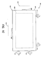
- FIG. 1A is a schematic top view of an exemplary embodiment of a substrate positioning system 101 in accordance with the present invention.
- the substrate positioning system 101 is positioned adjacent a support stage 103 that supports a substrate 105 having an edge 107.
- the substrate positioning system 101 includes a plurality of pushers 109 and stops 111 arranged in a spaced relation around the support stage 103.
- Each pusher 109 is adapted to assume a retracted position 113 such that the substrate 105 may be conveniently loaded onto and removed from the support stage 103 by one of a variety of loading/removing means (not shown), e.g. a human operator, or a robot utilizing an end effector to lower and/or lift the substrate 105 relative to the support stage 103, etc.
- Such adjustments may calibrate the position and the orientation of the substrate 105 relative to the support stage 103 so that, after the adjustment, the edge 107 of the substrate 105 will be aligned with a predefined x-y coordinate system 115 having a known position and orientation relative to the support stage 103 (e.g., a first vertically-oriented datum plane 117 (shown in profile), and a second vertically-oriented datum plane 119 (also shown in profile) substantially perpendicular to the first vertically-oriented datum plane 117).
- a predefined x-y coordinate system 115 having a known position and orientation relative to the support stage 103 (e.g., a first vertically-oriented datum plane 117 (shown in profile), and a second vertically-oriented datum plane 119 (also shown in profile) substantially perpendicular to the first vertically-oriented datum plane 117).
- the stops 111 of the substrate positioning system 101 occupy predefined positions and/or orientations relative to the support stage 103 so as to collectively define a substrate edge trap 121 that is aligned with the predefined x-y coordinate system 115 of the support stage 103.
- the substrate edge trap 121 is shaped to correspond to an edge of a substrate (e.g. the edge 107 of the substrate 105) to be loaded onto the support stage 103.
- FIG. 1B is a schematic top view of the exemplary embodiment of the substrate positioning system 101 of FIG. 1A wherein each pusher 109 is in contact with the edge 107 of the substrate 105.
- each pusher 109 is adapted to extend in the direction of the support stage 103 along a generally straight-line path (not shown) from the retracted position 113 associated with the pusher 109 and to contact a portion of the edge 107 of the substrate 105.
- Non-linear extension paths also may be employed.
- FIG. 1C is a schematic top view of the exemplary embodiment of the substrate positioning system 101 of FIG. 1A wherein the substrate 105, still supported by the support stage 103, has been calibrated to the support stage 103 by the substrate positioning system 101 such that the edge 107 of the substrate 105 is aligned with the predefined x-y coordinate system 115 (FIG. 1A) of the support stage 103.
- the substrate positioning system 101 may employ the pushing force of the pushers 109 to adjust the position of the substrate 105 relative to the support stage 103.
- the substrate positioning system 101 may move the substrate 105 from the position of FIG. 1A to the position of FIG. 1C.
- substrate positioning system 101 directs each pusher 109 to cease applying a pushing force (not shown) to the edge 107 of the substrate 105. Further, each pusher 109 thereafter may be directed to retract from the substrate 105 and the support stage 103 to the retracted position 113 associated with the pusher 109, as illustrated in FIG. 1A.
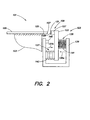
- FIG. 2 is a schematic side elevational view of an exemplary pushing device 123 in accordance with the present invention that may include the pusher 109 of the substrate positioning system 101 illustrated in FIGS. 1A-1C.
- the pushing device 123 is adapted to cause the pusher 109 to move toward the substrate 105 and/or the support stage 103 and move the substrate 105 relative to the support stage 103. (As shown in FIG.
- the support stage 103 may be coated with a low friction coating 125, such as Teflon® (e.g., polytetrafluoroethylene) or another similar material.)
- Teflon® e.g., polytetrafluoroethylene
- the pushing device 123 also is adapted to cause the pusher 109 to move away from the substrate 105 and/or the support stage 103, e.g. when a substrate is to be loaded onto or unloaded from the support stage 103.
- Each pusher 109 of the substrate positioning system 101 comprises a body 127, which in at least one embodiment may be rigid so as to facilitate precise adjustment of the position and orientation of the substrate 105.
- the body 127 of each pusher 109 may further comprise a pushing surface 129 adapted to contact the edge of a substrate (e.g. the edge 107 of the substrate 105).
- the pushing surface 129 of the body 127 of each pusher 109 may include a low friction coating 131 (e.g., Teflon® or the like). Such a low friction coating may be advantageous when a substrate must slide against a pusher 109 during positioning with the substrate positioning system 101 (described below).
- the pushing device 123 further comprises a pusher support 133 of FIG. 2 to which the pusher 109 is coupled, (e.g., at an elevation of the edge 107 of the substrate 105).
- the pusher 109 and the pusher support 133 are not separate parts of an assembly, but are separate features of a single part of unitary construction.
- the pushing device 123 also includes (1) a biasing device 135 adapted to contact and/or couple with the pusher support 133 and apply a biasing force (represented by arrow 135a) to the pusher support 133; (2) a bias-defeating device 137 adapted to contact and/or couple with the pusher support 133 and apply a retracting force (represented by arrow 137a) to the pusher support 133; and (3) a common frame 139 to which the biasing device 135 and the bias-defeating device 137 are mounted and against which the biasing device 135 and the bias-defeating device 137 are adapted to press during the generation and application of the respective biasing and retracting forces described above.
- a biasing device 135 adapted to contact and/or couple with the pusher support 133 and apply a biasing force (represented by arrow 135a) to the pusher support 133
- a bias-defeating device 137 adapted to contact and/or couple with the pusher support 133 and apply
- the biasing device 135 comprises a coil spring 141.
- the biasing device 135 may include an air cylinder, a Belleville washer, a leaf spring, etc.
- the bias-defeating device 137 comprises a bellows 143.
- the bias-defeating device 137 may include a motor driven lead screw or similar mechanism.
- the common frame 139 may be adapted to restrict the motion of the pusher 109 so as to prevent impact between the pusher 109 (and/or the pusher support 133) and the support stage 103.
- the common frame 139 may include a stop 145 adapted to contact the pusher support 133 and prevent the pusher support 133 from moving any further toward the support stage 103 and/or the substrate 105 once contact occurs.
- the pushing device 123 activates the bias-defeating device 137 to begin applying a retracting force to the pusher support 133, e.g. assuming the pusher support 133 is in an extended position (not shown) near the support stage 103 in FIG. 2 (this leftmost limit of the range of motion of the pusher support 133 of FIG. 2 is discussed further below).
- the retracting force must become larger than the biasing force of the biasing device 135 for the overall motive force of the pushing device 123 to cause the pusher 109 to begin to move away from the support stage 103 and/or the substrate 105. As the pusher 109 moves away from the support stage 103, the biasing device 135 becomes increasingly compressed.
- the behavior of the bias-defeating device 137 can be such that the pusher 109 moves relatively quickly away from the support stage 103, depending on the magnitude of the retracting force relative to the magnitude of the biasing force.
- the biasing force the biasing device 135 generates may increase.
- the bellows 143 can be inflated rapidly to cause the bellows 143 to quickly expand to move the pusher 109 away from the support stage 103.
- the pusher 109 may be moved away from the support stage 103 until the pusher 109 and/or the pusher support 133 reaches a limit of motion (e.g., the retracted position 113 for the pusher 109 as shown in FIG. 1A).
- This limit can be established in many different ways.
- the pusher support 133 may contact the common frame 139, or the coil spring 141 may reach a fully compressed state that prevents further motion of the pusher support 133.
- Those skilled in the art will recognized other ways to establish such a limit.
- Motion of the pusher 109 toward the support stage 103 occurs when the retracting force generated by the bias-defeating device 137 is weaker than the biasing force generated by the biasing device 135.
- Controlled motion of the pusher 109 toward the support stage 103 is preferred since contact with the edge 107 of the substrate 105 is preferably established when the pusher 109 moves at a relatively low speed (e.g., to preclude a damaging impact between the pusher 109 and the edge 107 of the substrate 105, or between stops 111 and the edge 107 of the substrate 105).
- Such controlled motion of the pusher 109 may be achieved, for example, by gradually reducing the retracting force of the bias-defeating device 137 such that the pusher 109 begins to move away from the retracted position 113 and toward the support stage 103 and/or the substrate 105 at a relatively slow speed.
- the bellows 143 can be deflated gradually to cause the magnitude of the retracting force generated by the bellows 143 to slowly lessen, and after the deflation has proceeded sufficiently, the biasing force generated by the biasing device 135 will dominate and cause the pusher 109 to move toward the support stage 103.
- the biasing force will be at its peak as the pusher 109 begins to move away from its retracted position, and will weaken thereafter as the coil spring 141 relaxes (e.g., continued deflation of the bellows 143 may be necessary for the biasing force to remain dominant as the coil spring 141 decompresses).
- the pusher 109 may be moved toward the support stage 103 direction, until the pusher 109 reaches a limit of motion in that direction.
- This limit may be established by the pushing force applied to the edge 107 of the substrate 105 by the pusher 109 being fully resisted by an equal and opposite force applied to the edge 107 of the substrate 105 by one or more of the stops 111 (FIG. 1A). Lacking such resistance from the stops 111, the motion limit of the pusher 109 may be established by the pusher support 133 directly contacting the stop 145 of the pushing device 123.
- the motion limit alternatively may be set by the bias-defeating device 137 reaching a fully compressed state that prevents further motion of the pusher support 133.
- Other ways of establishing a limit may be employed, such as via the use of sensors (FIG. 6) and a controller (FIG. 6) as described below.
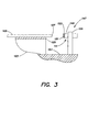
- FIG. 3 is a schematic side elevational view of an exemplary stopping device 147 in accordance with the present invention that may include the stop 111 of the substrate positioning system 101 illustrated in FIGS. 1A-1C.
- the stopping device 147 is adapted to situate the stop 111 at an elevation of the edge 107 of the substrate 105, confine the stop 111 to an orientation suitable for contact between the stop 111 and the edge 107 of the substrate 105, and brace the stop 111 (e.g., in circumstances when pushing forces associated with the pushers 109 are transmitted through the substrate 105 to the stop 111) so that the stop 111 maintains a predefined x-y position relative to the support stage 103.
- the substrate positioning system 101 comprises a plurality of the stopping devices 147, each stopping device 147 corresponding to one of the stops 111 (FIG. 1A).
- each stop 111 of the substrate positioning system 101 includes a body 149, which may have a stopping surface 151 adapted to contact the edge of a substrate (e.g. the edge 107 of the substrate 105).
- the stopping surface 151 of the body 149 of each stop 111 may include a low friction coating 153 (e.g., Teflon® of the like). Such a low friction coating may be advantageous when a substrate must slide against a stop 111 during positioning with the substrate positioning system 101 (described below).
- the stopping surface 151 of the stop 111 may be curved. In other embodiments, the stopping surface 151 of the stop 111 may be substantially flat. Other configurations may be employed.
- the stopping device 147 further comprises a stop support 155, to which the stop 111 is coupled (e.g., at an elevation of the edge 107 of the substrate 105).
- the stop support 155 may be affixed to, and extend upward from, a base 157 to which the support stage 103 is affixed.
- the stop support 155 may be coupled to the support stage 103.
- the stop support 155 occupies a substantially constant x-y position relative to the support stage 103 (e.g., to coincide with or define the x-y coordinate system 115 of FIG. 1A).
- the stop 111 is adapted to prevent the substrate 105 from moving relative to the support stage 103 any farther than a limit set by the stop 111 (e.g., when the edge 107 of the substrate 105 is in direct contact with the stopping surface 151 of the body 149 of the stop 111).
- the stopping device 147 is adapted to brace the stop 111 against pushing forces of the pushers 109 so as to substantially prevent movement of the stop 111 in response to the pushing forces.
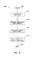
- FIG. 4 is a flowchart that illustrates an exemplary inventive process 400 for calibrating a substrate to a predefined coordinate system of a support stage while the support stage supports the substrate.
- the process 400 begins with a step 401.
- step 402 assuming the pushers 109 are in their retracted positions 113, the substrate 105 is loaded onto the support stage 103 (FIG. 1A).
- Step 402 may be accomplished via any appropriate means or processes, e.g.
- the substrate 105 is caused to rest on the support stage 103 at an appropriate preliminary position relative to the support stage 103, e.g., a position that enables the substrate positioning system 101 to subsequently adjust the position and/or orientation of the substrate 105 relative to the support stage 103.
- each pusher 109 is caused to extend toward the edge 107 of the substrate 105 as necessary so as to achieve contact with the edge 107 of the substrate 105.
- each pushing device 123 causes the biasing force 135a generated by the biasing device 135 (FIG. 2) to dominate any retracting force 137a generated by the bias-defeating device 137 (FIG. 2).
- the pressure within the bellows 143 may be reduced to decrease the retracting force that otherwise holds each pusher 109 in the retracted position 113. In this manner, each pusher 109 will move toward the edge 107 of the substrate 105.
- each pusher 109 of the substrate positioning system 101 contacts the edge 107 of the substrate 105.
- the pushers 109 need not contact the edge 107 of the substrate 105 simultaneously, e.g. as each pusher 109 extends through whatever distance is necessary to achieve contact with that portion of the edge 107 of the substrate 105 which lies in the path of that pusher 109.
- step 404 once contact is achieved between a particular pusher 109 and the edge 107 of the substrate 105 (step 404), that pusher 109 remains in substantially continuous contact with the edge 107 of the substrate 105 during any subsequent motion between the substrate 105 and the support stage 103.
- step 404 once contact is achieved between a particular pusher 109 and the edge 107 of the substrate 105 (step 404), subsequent interruptions in contact between that pusher 109 and the edge 107 of the substrate 105 during motion between the substrate 105 and the support stage 103 may occur.
- each pusher 109 continues to extend as necessary so as to cause the position of the substrate 105 relative to the support stage 103 to become calibrated to the predefined x-y coordinate system 115 of the support stage 103.
- each pushing device 123 of the substrate positioning system 101 may cause its respective pusher 109 to extend until the edge 107 of the substrate 105 opposite the pusher 109 contacts and/or is pressed against the stops 111 toward which the pusher 109 travels during positioning of the substrate 105 on the support stage 103.
- the substrate 105 may be trapped or "gripped" between the pusher 109 and one or more stops 111 of the substrate positioning system 101.
- step 406 the process 400 concludes.
- one or more of the pushers 109, or all of the pushers 109 may be caused to individually retract to their respective retracted position 113 at the conclusion of the process 400 in preparation for a subsequent unloading of the substrate 105 from the support stage 103.
- the pushing forces generated by one or more of the pushers 109 on the edge 107 of the substrate 105 can be continued, e.g. to ensure proper positioning of the substrate 105 relative to the support stage 103 during a subsequent processing step, such as an e-beam search, or a defect detection routine.
- steps 401-406 of the process 400 may be performed by a controller (not shown) that is operable to control positioning of each pusher 109 (e.g., by controlling gas flow to/from the bellows 143 of each pushing device 123). Further, one or more of the steps 401-406 may be implemented as one or more computer program products stored in a suitable computer readable medium (e.g., a carrier wave signal, hard drive, random access memory, etc.)
- a suitable computer readable medium e.g., a carrier wave signal, hard drive, random access memory, etc.
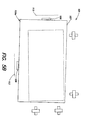
- FIG. 5A is a schematic top view of the substrate positioning system 101 of FIGS. 1A-1C, wherein a substrate 105a is misaligned with the support stage 103 following loading onto the support stage 103.
- the substrate positioning system 101 may still calibrate the position and/or the orientation of the substrate 105a relative to the support stage 103 so that the edge 107 of the substrate 105a is aligned with the predefined x-y coordinate system 115 (FIG. 1A).
- FIG. 5B is a schematic top view of the substrate positioning system 101 of FIG. 5A wherein each pusher 109 is in contact with the edge 107 of the substrate 105a.
- the orientation of each pusher 109 is fixed relative to the direction in which the pusher 109 extends from the retracted position 113 associated with that pusher 109.
- at least the initial contact between each pusher 109 and the edge 107 of the substrate 105a is characterized by a misalignment between that pusher 109 and the portion of the edge 107 of the substrate 105a contacted by that pusher 109.
- the orientation of each pusher 109 relative to a direction in which the pusher extends need not be fixed).
- FIG. 5C is a schematic top view of the substrate positioning system 101 of FIG. 5A wherein the substrate 105a, still supported by the support stage 103, has been calibrated to the support stage 103 by the substrate positioning system 101 such that the edge 107 of the substrate 105a is aligned with the predefined x-y coordinate system 115 (FIG. 1A) of the support stage 103.
- the misalignment relative to the support stage 103 that characterized the substrate 105a as shown in FIGS. 5A-5B is corrected.
- the exemplary embodiment of the substrate positioning system 101 illustrated in FIGS. 5A-5C permits sliding linear communication between each pusher 109 and the edge 107 of the substrate 105a, and permits sliding communication (e.g.
- each stop 111 sliding linear communication between each stop 111 and the edge 107 of the substrate 105a, so as to adjust the overall orientation of the substrate 105a (e.g., allowing alignment of the edge 107 of the substrate 105a with the predefined x-y coordinate system 115 (FIG. 1A) of the support stage 103).
- each pusher 109 may be subjected to a separate and unique biasing force, and adapted to extend in different directions of extension, as well as through different extension distances as necessary, such that substrates of differing sizes and/or proportions, and of differing degrees of initial orientation relative to the support stage 103, can be calibrated to the predefined x-y coordinate system 115 (FIG. 1A) of the support stage 103 to substantially the same degree of precision.
- FIG. 6 is a schematic side elevational view of an alternative pushing device 123a in accordance with the present invention.
- the pushing device 123a of FIG. 6 is similar to the pushing device 123 of FIG. 2.
- the pushing device 123a comprises a pusher 109, a pusher support 133, a biasing device 135, a bias-defeating device 137 and a common frame 139, as does the pushing device 123 of FIG. 2.
- the pushing device 123a further comprises a guideshaft 159 adapted to rotate (e.g., within bearings (not shown) in the common frame 139) and to support and guide the pusher support 133 as the pusher support 133 moves relative to the common frame 139 of the pushing device 123a.
- a sensor 161 may be provided, coupled to the common frame 139, for example, and adapted to generate a signal and/or signals corresponding to the speed of rotation and/or the rotational position of the guideshaft 159.
- the exemplary embodiment of FIG. 6 further comprises a controller 163 adapted to receive the signal and/or signals from the sensor 161 and to determine a position of the pusher 109 relative to the support stage 103 based thereon.
- the biasing device 135 and the bias-defeating device 137 are aligned in common with the guideshaft 159 so as to encourage smooth motion of the pusher support 133 relative to the common frame 139, and/or to eliminate at least one source of torque in the pushing device 123a.
- the guideshaft 159 may comprise, for example, a lead screw or the like.
Landscapes
- Physics & Mathematics (AREA)
- General Physics & Mathematics (AREA)
- Engineering & Computer Science (AREA)
- Architecture (AREA)
- Mechanical Engineering (AREA)
- Civil Engineering (AREA)
- Structural Engineering (AREA)
- Life Sciences & Earth Sciences (AREA)
- Sustainable Development (AREA)
- Health & Medical Sciences (AREA)
- Environmental & Geological Engineering (AREA)
- Epidemiology (AREA)
- Public Health (AREA)
- Container, Conveyance, Adherence, Positioning, Of Wafer (AREA)
Abstract
Description
Alternatively, the pushing forces generated by one or more of the
Claims (31)
- A substrate positioning system adapted to adjust a position of an edge of a substrate relative to a stage that supports the substrate, comprising:a plurality of pushing devices and stops arranged in a spaced relation around a stage that is adapted to support a substrate, wherein each stop occupies a fixed position relative to the stage and each pushing device comprises a movable pusher that is adapted to:extend toward an edge of the substrate that is supported by the stage;contact the edge of the substrate while the substrate is supported by the stage; andcontinue extending so as to cause the substrate to translate relative to the stage toward one or more of the stops until the substrate contacts the one or more stops.
- The substrate positioning system of claim 1, wherein each pushing device is adapted to:cause the pusher of the pushing device to extend toward the edge of the substrate that is supported by the stage;cause the pusher of the pushing device to contact the edge of the substrate while the substrate is supported by the stage; andcause the pusher of the pushing device to continue extending so as to cause the substrate to translate relative to the stage toward one or more of the stops until the substrate contacts the one or more stops.
- The substrate positioning system of claim 1 or claim 2 wherein:the pusher of each pushing device is further adapted to retract from the edge of the substrate; andeach pushing device is further adapted to cause the pusher of the pushing device to retract from the edge of the substrate.
- The substrate positioning system according to any one of the claims 1 to 3 further comprising a controller coupled to each pushing device, and adapted to:cause the pusher of each pushing device to extend toward the edge of the substrate that is supported by the stage;cause the pusher of each pushing device to contact the edge of the substrate while the substrate is supported by the stage; andcause the pusher of each pushing device to continue extending so as to cause the substrate to translate relative to the stage toward one or more of the stops until the substrate contacts the one or more stops.
- The substrate positioning system according to any one of the claims 1 to 4 , wherein each pusher is further adapted to extend toward the edge of the substrate along a straight-line path.
- The substrate positioning system according to any one of the claims 1 to 5, wherein the plurality of pushing devices reside in a common plane containing the straight-line paths of the pushers.
- The substrate positioning system according to any one of the claims 1 to 6, wherein the plurality of pushing devices include a first pushing device oriented such that the pusher of the first pushing device extends in a first direction, and a second pushing device oriented such that the pusher of the second pushing device extends in a second direction substantially perpendicular to the first direction.
- The substrate positioning system according to any one of the claims 1 to 7, wherein each pushing device further comprises a biasing device coupled to the pusher of the pushing device and adapted to move the pusher toward the edge of the substrate.
- The substrate positioning system of claim 8, wherein the biasing device comprises a spring.
- The substrate positioning system according to any one of the claims 1 to 9, wherein each pushing device further comprises a retracting device coupled to the pusher of the pushing device and adapted to counteract the biasing device so as to move the pusher away from the edge of the substrate.
- A pushing device, comprising:a pusher adapted to:extend toward an edge of a substrate that is supported by a stage;contact the edge of the substrate while the substrate is supported by the stage; andcontinue extending so as to cause the substrate to translate relative to the stage toward one or more stops until the substrate contacts the one or more stops.
- The pushing device of claim 11further comprising:a biasing device adapted to apply a biasing force to the pusher; anda bias-defeating device adapted to apply a retracting force to the pusher so as to counteract the biasing force of the biasing device.
- The pushing device according to any one of the claims 11 to 12 further comprising a common frame coupled to the biasing device and the bias-defeating device.
- The pushing device of claim 13 wherein the common frame is adapted to restrict motion of the pusher so as to prevent impact between the pusher and the stage.
- The pushing device according to any one of the claims 11 to 14 further comprising a pusher support coupled to the pusher.
- The pushing device according to any one of the claims 11 to 15 further comprising a guideshaft adapted to support and guide the pusher support.
- The pushing device according to any one of the claims 11 to 16 further comprising a sensor adapted to generate a signal corresponding to at least one of a speed of rotation of the guideshaft and a rotational position of the guideshaft.
- The pushing device according to any one of the claims 11 to 17 further comprising a controller adapted to:receive the signal from the sensor; anddetermine a position of the pusher relative to the stage based on the signal.
- A stopping device, comprising:a stop adapted to prevent a substrate from moving relative to a support stage; anda stopping device coupled to the stop, and adapted to brace the stop against pushing forces exerted against an edge of the substrate so as to substantially prevent movement of the stop in response to the pushing forces.
- The stopping device of claim 19 wherein the stopping device is further adapted to:situate the stop at an elevation of an edge of a substrate; andbrace the stop so that the stop maintains a predefined x-y position relative to the stage.
- A method of adjusting a position of a substrate relative to a stage that supports the substrate, comprising:providing a plurality of pushers and stops in a spaced relation around a stage that is adapted to support a substrate;causing each pusher to extend toward an edge of the substrate;causing each pusher to contact the edge of the substrate; andcausing each pusher to continue extending so as to cause the substrate to translate relative to the stage toward one or more of the stops until the substrate contacts the one or more stops.
- The method of claim 21 wherein causing each pusher to extend toward an edge of the substrate includes causing a biasing force applied to each pusher to dominate a retracting force applied to each pusher.
- The method of claim 21 or claim 22 wherein causing each pusher to continue extending so as to cause the substrate to translate relative to the stage toward one or more of the stops until the substrate contacts the one or more stops includes causing the position of the substrate relative to the stage to be calibrated to an x-y coordinate system of the stage.
- The method according to any one of the claims 21 to 23 further comprising causing one or more of the plurality of pushers to retract.
- The method according to any one of the claims 21 to 24 further comprising loading a substrate on the support.
- The method of claim 25 wherein the substrate is misaligned with the stage.
- The method of claim 25 or claim 26 further comprising:permitting sliding communication between each pusher and the edge of the substrate; andpermitting sliding communication between each stop and the edge of the substrate.
- A computer program product comprising:a medium readable by a computer, the computer readable medium having computer program code adapted to:cause a plurality of pushers to extend toward an edge of a substrate, wherein the plurality of pushers and a plurality of stops are provided in a spaced relation around a stage that is adapted to support the substrate;cause each pusher to extend toward the edge of the substrate;cause each pusher to contact the edge of the substrate; andcause each pusher to continue extending so as to cause the substrate to translate relative to the stage toward one or more of the stops until the substrate contacts the one or more stops.
- The computer program product of claim 28 wherein the computer program code is further adapted to cause a biasing force applied to each pusher to dominate a retracting force applied to each pusher by reducing the retracting force.
- The computer program product of claim 28 or claim 29 wherein the computer program code is further adapted to cause the position of the substrate relative to the stage to become calibrated to an x-y coordinate system of the stage.
- The computer program product according to any one of the claims 28 to 30 wherein the computer program code is further adapted to cause one or more of the plurality of pushers to retract by increasing the retracting force.
Applications Claiming Priority (2)
| Application Number | Priority Date | Filing Date | Title |
|---|---|---|---|
| US44897203P | 2003-02-20 | 2003-02-20 | |
| US448972P | 2003-02-20 |
Publications (2)
| Publication Number | Publication Date |
|---|---|
| EP1450398A2 true EP1450398A2 (en) | 2004-08-25 |
| EP1450398A3 EP1450398A3 (en) | 2004-11-10 |
Family
ID=32736527
Family Applications (1)
| Application Number | Title | Priority Date | Filing Date |
|---|---|---|---|
| EP04003863A Withdrawn EP1450398A3 (en) | 2003-02-20 | 2004-02-20 | A method and an apparatus for positioning a substrate relative to a support stage |
Country Status (5)
| Country | Link |
|---|---|
| EP (1) | EP1450398A3 (en) |
| JP (1) | JP4615877B2 (en) |
| KR (1) | KR100648335B1 (en) |
| CN (1) | CN1333453C (en) |
| TW (1) | TWI285937B (en) |
Cited By (7)
| Publication number | Priority date | Publication date | Assignee | Title |
|---|---|---|---|---|
| WO2006090870A3 (en) * | 2005-02-25 | 2007-10-25 | Fujifilm Corp | Image forming device and method |
| WO2010121702A1 (en) * | 2009-04-25 | 2010-10-28 | Ev Group Gmbh | Device for aligning and pre-attaching a wafer |
| CN103100902A (en) * | 2012-11-15 | 2013-05-15 | 无锡市航鹄科技有限公司 | Multifunctional milling combination positioning tool |
| CN103286603A (en) * | 2013-05-14 | 2013-09-11 | 浙江山海机械有限公司 | Fixture for turning thin aluminum valve plate |
| CN103433885A (en) * | 2013-08-30 | 2013-12-11 | 中国电子科技集团公司第二十六研究所 | Large-area scintillation crystal array assembling device and assembling method thereof |
| US20140077431A1 (en) * | 2012-09-20 | 2014-03-20 | Varian Semiconductor Equipment Associates, Inc. | System and Method for 2D Workpiece Alignment |
| CN103713478A (en) * | 2013-12-31 | 2014-04-09 | 四川聚能核技术工程有限公司 | Pre-alignment device |
Families Citing this family (29)
| Publication number | Priority date | Publication date | Assignee | Title |
|---|---|---|---|---|
| JP4887630B2 (en) * | 2005-02-24 | 2012-02-29 | 日本電気硝子株式会社 | Glass substrate positioning device and end surface grinding device |
| DE102007052027B3 (en) | 2007-10-31 | 2009-04-16 | Grenzebach Maschinenbau Gmbh | Method and device for the contamination-free treatment of shock-sensitive glass plates in clean rooms |
| DE102007052183A1 (en) | 2007-10-31 | 2009-06-25 | Grenzebach Maschinenbau Gmbh | Apparatus and method for aligning shock-sensitive glass plates in clean rooms |
| KR100942066B1 (en) * | 2008-04-30 | 2010-02-11 | 주식회사 테라세미콘 | Holder stage |
| KR101569796B1 (en) * | 2009-06-23 | 2015-11-20 | 주성엔지니어링(주) | Substrate alignment apparatus, substrate processing apparatus including same, and substrate alignment method |
| JP2011098430A (en) * | 2009-11-09 | 2011-05-19 | Sharp Corp | Positioning device |
| CN102841505B (en) * | 2011-06-22 | 2015-06-17 | 上海微电子装备有限公司 | Substrate-precise-positioning workpiece stage |
| CN202257028U (en) * | 2011-09-13 | 2012-05-30 | 深圳市华星光电技术有限公司 | Lcd exposure platform device and exposure system |
| KR101373209B1 (en) * | 2011-12-16 | 2014-04-14 | (재)경북차량용임베디드기술연구원 | Align apparatus for glass grinder |
| CN103206971B (en) * | 2012-01-11 | 2017-02-01 | 昆山允升吉光电科技有限公司 | Method for locating electric object stage |
| CN103206977B (en) * | 2012-01-11 | 2016-12-14 | 昆山允升吉光电科技有限公司 | The object stage of Electronic control position |
| CN103203726B (en) * | 2012-01-11 | 2016-08-10 | 昆山允升吉光电科技有限公司 | Accurately control the object stage of position |
| CN103203725B (en) * | 2012-01-11 | 2016-08-10 | 昆山允升吉光电科技有限公司 | Accurately control the object stage of position |
| CN103206975B (en) * | 2012-01-11 | 2017-06-06 | 昆山允升吉光电科技有限公司 | Electric control object stage |
| CN102796998B (en) * | 2012-07-31 | 2013-11-27 | 桂林电子科技大学 | Method for operating and controlling position of nano-grating deposition substrate in vacuum vessel and device therefor |
| JP2014061561A (en) * | 2012-09-20 | 2014-04-10 | Yaskawa Electric Corp | Robot system and article manufacturing method |
| CN103323960B (en) * | 2013-05-15 | 2016-03-30 | 友达光电(苏州)有限公司 | Locating device and use its pick-up unit, apparatus for assembling |
| CN103624605A (en) * | 2013-12-04 | 2014-03-12 | 苏州鑫叶自动化设备系统有限公司 | TV (television) frame-machining fixture |
| CN103752576B (en) * | 2014-01-14 | 2015-11-18 | 无锡江南计算技术研究所 | A kind of eccentric cleaning General purpose jig |
| KR101449905B1 (en) * | 2014-06-18 | 2014-10-13 | 이승해 | Glass thermal transferring apparatus for display device capable of adjusting glass position |
| TWI668795B (en) * | 2014-09-15 | 2019-08-11 | 美商瓦里安半導體設備公司 | Active substrate alignment system for semiconductor processing and method for aligning substrate |
| CN104459439B (en) * | 2014-12-08 | 2019-02-19 | 昆山精讯电子技术有限公司 | The automatic checkout equipment of touch screen |
| CN104992919B (en) | 2015-07-21 | 2017-11-07 | 合肥鑫晟光电科技有限公司 | Angle, positioner and position are reformed method |
| KR101650398B1 (en) * | 2015-09-11 | 2016-08-24 | (주)코맷 | Wafer centering device for measuring instrument |
| CN106064880B (en) * | 2016-06-27 | 2019-09-17 | 昆山国显光电有限公司 | Positioning device and its localization method |
| CN108153008B (en) * | 2018-01-18 | 2021-03-02 | 武汉华星光电技术有限公司 | Substrate clamping and aligning device |
| TWI890340B (en) * | 2019-03-13 | 2025-07-11 | 以色列商核心流有限公司 | Circular wafer lateral positioning device |
| CN111863664B (en) * | 2020-07-29 | 2022-02-25 | 北京七星华创集成电路装备有限公司 | Substrate reforming device and semiconductor processing equipment |
| CN120221430A (en) * | 2023-12-26 | 2025-06-27 | 北京北方华创微电子装备有限公司 | Wafer transfer chamber, semiconductor process equipment and wafer calibration method |
Family Cites Families (13)
| Publication number | Priority date | Publication date | Assignee | Title |
|---|---|---|---|---|
| US5374147A (en) * | 1982-07-29 | 1994-12-20 | Tokyo Electron Limited | Transfer device for transferring a substrate |
| US4628986A (en) * | 1985-03-26 | 1986-12-16 | Combustion Engineering, Inc. | Molding register system |
| JPH07114233B2 (en) * | 1992-04-01 | 1995-12-06 | 株式会社ニコン | Board positioning device |
| JPH0689845A (en) * | 1992-09-08 | 1994-03-29 | Nikon Corp | Substrate positioning device |
| JP3146395B2 (en) * | 1993-01-29 | 2001-03-12 | ローム株式会社 | Liquid crystal cell positioning device |
| JPH07276170A (en) * | 1994-03-31 | 1995-10-24 | Canon Inc | Positioning device and printing apparatus provided with the positioning device |
| CN2222404Y (en) * | 1995-04-24 | 1996-03-13 | 郭光华 | Automatic pin insertion machine for electronic connector |
| JPH08313815A (en) * | 1995-05-23 | 1996-11-29 | Olympus Optical Co Ltd | Positioning and holding device for substrate member |
| JP2710230B2 (en) * | 1995-06-07 | 1998-02-10 | 日本電気株式会社 | Board crack detection device |
| US5980195A (en) * | 1996-04-24 | 1999-11-09 | Tokyo Electron, Ltd. | Positioning apparatus for substrates to be processed |
| WO1998028665A1 (en) * | 1996-12-24 | 1998-07-02 | Koninklijke Philips Electronics N.V. | Two-dimensionally balanced positioning device with two object holders, and lithographic device provided with such a positioning device |
| US20020051697A1 (en) * | 2000-07-08 | 2002-05-02 | Ko Alexander Sou-Kang | Removable gripper pads |
| JP2002308420A (en) * | 2001-04-10 | 2002-10-23 | Canon Inc | Glass substrate positioning device |
-
2004
- 2004-02-20 JP JP2004045387A patent/JP4615877B2/en not_active Expired - Fee Related
- 2004-02-20 CN CNB2004100313695A patent/CN1333453C/en not_active Expired - Fee Related
- 2004-02-20 EP EP04003863A patent/EP1450398A3/en not_active Withdrawn
- 2004-02-20 KR KR1020040011386A patent/KR100648335B1/en not_active Expired - Fee Related
- 2004-02-20 TW TW093104366A patent/TWI285937B/en not_active IP Right Cessation
Cited By (17)
| Publication number | Priority date | Publication date | Assignee | Title |
|---|---|---|---|---|
| WO2006090870A3 (en) * | 2005-02-25 | 2007-10-25 | Fujifilm Corp | Image forming device and method |
| WO2010121702A1 (en) * | 2009-04-25 | 2010-10-28 | Ev Group Gmbh | Device for aligning and pre-attaching a wafer |
| KR20120014557A (en) * | 2009-04-25 | 2012-02-17 | 에베 그룹 게엠베하 | Device for Aligning and Prefixing Wafers |
| CN102439711A (en) * | 2009-04-25 | 2012-05-02 | Ev集团有限责任公司 | Devices for alignment and pre-fixation of wafers |
| CN102439711B (en) * | 2009-04-25 | 2017-02-08 | Ev集团有限责任公司 | Devices for alignment and pre-fixation of wafers |
| US9449863B2 (en) | 2009-04-25 | 2016-09-20 | Ev Group Gmbh | Device for aligning and pre-fixing a wafer |
| KR101642536B1 (en) | 2009-04-25 | 2016-07-25 | 에베 그룹 게엠베하 | Device for aligning and pre-attaching a wafer |
| US8918989B2 (en) | 2009-04-25 | 2014-12-30 | Ev Group Gmbh | Device for aligning and pre-fixing a wafer |
| US20140077431A1 (en) * | 2012-09-20 | 2014-03-20 | Varian Semiconductor Equipment Associates, Inc. | System and Method for 2D Workpiece Alignment |
| US9082799B2 (en) * | 2012-09-20 | 2015-07-14 | Varian Semiconductor Equipment Associates, Inc. | System and method for 2D workpiece alignment |
| CN103100902A (en) * | 2012-11-15 | 2013-05-15 | 无锡市航鹄科技有限公司 | Multifunctional milling combination positioning tool |
| CN103286603B (en) * | 2013-05-14 | 2016-01-06 | 浙江山海机械有限公司 | A kind of frock clamp of turnery processing book sheet aluminium valve plate |
| CN103286603A (en) * | 2013-05-14 | 2013-09-11 | 浙江山海机械有限公司 | Fixture for turning thin aluminum valve plate |
| CN103433885B (en) * | 2013-08-30 | 2015-11-11 | 中国电子科技集团公司第二十六研究所 | Large-area scintillation crystal array apparatus for assembling and assemble method thereof |
| CN103433885A (en) * | 2013-08-30 | 2013-12-11 | 中国电子科技集团公司第二十六研究所 | Large-area scintillation crystal array assembling device and assembling method thereof |
| CN103713478A (en) * | 2013-12-31 | 2014-04-09 | 四川聚能核技术工程有限公司 | Pre-alignment device |
| CN103713478B (en) * | 2013-12-31 | 2017-02-01 | 四川聚能核技术工程有限公司 | Pre-alignment device |
Also Published As
| Publication number | Publication date |
|---|---|
| TW200428562A (en) | 2004-12-16 |
| JP2004253808A (en) | 2004-09-09 |
| CN1536640A (en) | 2004-10-13 |
| TWI285937B (en) | 2007-08-21 |
| KR100648335B1 (en) | 2006-11-23 |
| JP4615877B2 (en) | 2011-01-19 |
| KR20040075291A (en) | 2004-08-27 |
| CN1333453C (en) | 2007-08-22 |
| EP1450398A3 (en) | 2004-11-10 |
Similar Documents
| Publication | Publication Date | Title |
|---|---|---|
| EP1450398A2 (en) | A method and an apparatus for positioning a substrate relative to a support stage | |
| US7104535B2 (en) | Methods and apparatus for positioning a substrate relative to a support stage | |
| KR20050118682A (en) | Methods and apparatus for high speed object handling | |
| JPH06177229A (en) | Method and apparatus for coincident and jamless alignment of semiconductor wafer | |
| JP2008006439A (en) | Head unit of paste dispenser | |
| US7499767B2 (en) | Methods and apparatus for positioning a substrate relative to a support stage | |
| US7151981B2 (en) | Methods and apparatus for positioning a substrate relative to a support stage | |
| US6381002B1 (en) | Process for controlling a gap between a mask and a workpiece in proximity exposure and a proximity exposure device | |
| JP5295259B2 (en) | Pre-aligner device | |
| KR100587781B1 (en) | Methods and apparatus for positioning a substrate relative to a support stage | |
| JPH07221167A (en) | Method for co-aligning semiconductor wafers processed in one or more blind processing modules | |
| CN101738870A (en) | Proximity exposure apparatus, method of delivering a mask of a proximity exposure apparatus and method of manufacturing a display panel substrate | |
| JP2006120861A (en) | Tilt correction device and transfer robot provided with the same | |
| JP4835839B2 (en) | Transfer robot and position correction method for transfer robot | |
| JPH0758186A (en) | Apparatus and method for consistent jam-free alignment of notched semiconductor wafers | |
| JPH0637170A (en) | Wafer alignment method and apparatus | |
| JPH11221784A (en) | Aligning method and device | |
| JP2005203661A (en) | Method and apparatus for measuring thin plate material | |
| KR100834116B1 (en) | Teaching Method of Semiconductor Manufacturing Equipment | |
| TWI893938B (en) | Centering device, centering method and substrate processing apparatus | |
| JP2001157931A (en) | Substrate positioning device | |
| KR102644399B1 (en) | Substrate cleaning apparatus | |
| KR20250042075A (en) | Substrate holding apparatus, substrate processing apparatus, separation method, and article manufacturing method | |
| WO2026053563A1 (en) | Cutting method and cutting system for brittle substrate | |
| KR19980022565A (en) | Semiconductor Wafer Alignment Device |
Legal Events
| Date | Code | Title | Description |
|---|---|---|---|
| PUAI | Public reference made under article 153(3) epc to a published international application that has entered the european phase |
Free format text: ORIGINAL CODE: 0009012 |
|
| 17P | Request for examination filed |
Effective date: 20040220 |
|
| AK | Designated contracting states |
Kind code of ref document: A2 Designated state(s): AT BE BG CH CY CZ DE DK EE ES FI FR GB GR HU IE IT LI LU MC NL PT RO SE SI SK TR |
|
| AX | Request for extension of the european patent |
Extension state: AL LT LV MK |
|
| PUAL | Search report despatched |
Free format text: ORIGINAL CODE: 0009013 |
|
| AK | Designated contracting states |
Kind code of ref document: A3 Designated state(s): AT BE BG CH CY CZ DE DK EE ES FI FR GB GR HU IE IT LI LU MC NL PT RO SE SI SK TR |
|
| AX | Request for extension of the european patent |
Extension state: AL LT LV MK |
|
| AKX | Designation fees paid | ||
| REG | Reference to a national code |
Ref country code: DE Ref legal event code: 8566 |
|
| STAA | Information on the status of an ep patent application or granted ep patent |
Free format text: STATUS: THE APPLICATION IS DEEMED TO BE WITHDRAWN |
|
| 18D | Application deemed to be withdrawn |
Effective date: 20050511 |