EP1450337A2 - Anzeigetafeltreiber mit Verarbeitungsfunktion für mehrere Graustufen - Google Patents
Anzeigetafeltreiber mit Verarbeitungsfunktion für mehrere Graustufen Download PDFInfo
- Publication number
- EP1450337A2 EP1450337A2 EP04003062A EP04003062A EP1450337A2 EP 1450337 A2 EP1450337 A2 EP 1450337A2 EP 04003062 A EP04003062 A EP 04003062A EP 04003062 A EP04003062 A EP 04003062A EP 1450337 A2 EP1450337 A2 EP 1450337A2
- Authority
- EP
- European Patent Office
- Prior art keywords
- display
- pixel
- pixel data
- discharge cells
- display lines
- Prior art date
- Legal status (The legal status is an assumption and is not a legal conclusion. Google has not performed a legal analysis and makes no representation as to the accuracy of the status listed.)
- Withdrawn
Links
Images


Classifications
-
- G—PHYSICS
- G09—EDUCATION; CRYPTOGRAPHY; DISPLAY; ADVERTISING; SEALS
- G09G—ARRANGEMENTS OR CIRCUITS FOR CONTROL OF INDICATING DEVICES USING STATIC MEANS TO PRESENT VARIABLE INFORMATION
- G09G3/00—Control arrangements or circuits, of interest only in connection with visual indicators other than cathode-ray tubes
- G09G3/20—Control arrangements or circuits, of interest only in connection with visual indicators other than cathode-ray tubes for presentation of an assembly of a number of characters, e.g. a page, by composing the assembly by combination of individual elements arranged in a matrix no fixed position being assigned to or needed to be assigned to the individual characters or partial characters
- G09G3/2007—Display of intermediate tones
- G09G3/2018—Display of intermediate tones by time modulation using two or more time intervals
- G09G3/2022—Display of intermediate tones by time modulation using two or more time intervals using sub-frames
- G09G3/204—Display of intermediate tones by time modulation using two or more time intervals using sub-frames the sub-frames being organized in consecutive sub-frame groups
-
- G—PHYSICS
- G09—EDUCATION; CRYPTOGRAPHY; DISPLAY; ADVERTISING; SEALS
- G09G—ARRANGEMENTS OR CIRCUITS FOR CONTROL OF INDICATING DEVICES USING STATIC MEANS TO PRESENT VARIABLE INFORMATION
- G09G3/00—Control arrangements or circuits, of interest only in connection with visual indicators other than cathode-ray tubes
- G09G3/20—Control arrangements or circuits, of interest only in connection with visual indicators other than cathode-ray tubes for presentation of an assembly of a number of characters, e.g. a page, by composing the assembly by combination of individual elements arranged in a matrix no fixed position being assigned to or needed to be assigned to the individual characters or partial characters
- G09G3/22—Control arrangements or circuits, of interest only in connection with visual indicators other than cathode-ray tubes for presentation of an assembly of a number of characters, e.g. a page, by composing the assembly by combination of individual elements arranged in a matrix no fixed position being assigned to or needed to be assigned to the individual characters or partial characters using controlled light sources
- G09G3/28—Control arrangements or circuits, of interest only in connection with visual indicators other than cathode-ray tubes for presentation of an assembly of a number of characters, e.g. a page, by composing the assembly by combination of individual elements arranged in a matrix no fixed position being assigned to or needed to be assigned to the individual characters or partial characters using controlled light sources using luminous gas-discharge panels, e.g. plasma panels
- G09G3/288—Control arrangements or circuits, of interest only in connection with visual indicators other than cathode-ray tubes for presentation of an assembly of a number of characters, e.g. a page, by composing the assembly by combination of individual elements arranged in a matrix no fixed position being assigned to or needed to be assigned to the individual characters or partial characters using controlled light sources using luminous gas-discharge panels, e.g. plasma panels using AC panels
- G09G3/291—Control arrangements or circuits, of interest only in connection with visual indicators other than cathode-ray tubes for presentation of an assembly of a number of characters, e.g. a page, by composing the assembly by combination of individual elements arranged in a matrix no fixed position being assigned to or needed to be assigned to the individual characters or partial characters using controlled light sources using luminous gas-discharge panels, e.g. plasma panels using AC panels controlling the gas discharge to control a cell condition, e.g. by means of specific pulse shapes
-
- G—PHYSICS
- G09—EDUCATION; CRYPTOGRAPHY; DISPLAY; ADVERTISING; SEALS
- G09G—ARRANGEMENTS OR CIRCUITS FOR CONTROL OF INDICATING DEVICES USING STATIC MEANS TO PRESENT VARIABLE INFORMATION
- G09G3/00—Control arrangements or circuits, of interest only in connection with visual indicators other than cathode-ray tubes
- G09G3/20—Control arrangements or circuits, of interest only in connection with visual indicators other than cathode-ray tubes for presentation of an assembly of a number of characters, e.g. a page, by composing the assembly by combination of individual elements arranged in a matrix no fixed position being assigned to or needed to be assigned to the individual characters or partial characters
- G09G3/2007—Display of intermediate tones
- G09G3/2018—Display of intermediate tones by time modulation using two or more time intervals
- G09G3/2022—Display of intermediate tones by time modulation using two or more time intervals using sub-frames
- G09G3/2025—Display of intermediate tones by time modulation using two or more time intervals using sub-frames the sub-frames having all the same time duration
-
- G—PHYSICS
- G09—EDUCATION; CRYPTOGRAPHY; DISPLAY; ADVERTISING; SEALS
- G09G—ARRANGEMENTS OR CIRCUITS FOR CONTROL OF INDICATING DEVICES USING STATIC MEANS TO PRESENT VARIABLE INFORMATION
- G09G3/00—Control arrangements or circuits, of interest only in connection with visual indicators other than cathode-ray tubes
- G09G3/20—Control arrangements or circuits, of interest only in connection with visual indicators other than cathode-ray tubes for presentation of an assembly of a number of characters, e.g. a page, by composing the assembly by combination of individual elements arranged in a matrix no fixed position being assigned to or needed to be assigned to the individual characters or partial characters
- G09G3/2007—Display of intermediate tones
- G09G3/2044—Display of intermediate tones using dithering
- G09G3/2051—Display of intermediate tones using dithering with use of a spatial dither pattern
- G09G3/2055—Display of intermediate tones using dithering with use of a spatial dither pattern the pattern being varied in time
-
- G—PHYSICS
- G09—EDUCATION; CRYPTOGRAPHY; DISPLAY; ADVERTISING; SEALS
- G09G—ARRANGEMENTS OR CIRCUITS FOR CONTROL OF INDICATING DEVICES USING STATIC MEANS TO PRESENT VARIABLE INFORMATION
- G09G3/00—Control arrangements or circuits, of interest only in connection with visual indicators other than cathode-ray tubes
- G09G3/20—Control arrangements or circuits, of interest only in connection with visual indicators other than cathode-ray tubes for presentation of an assembly of a number of characters, e.g. a page, by composing the assembly by combination of individual elements arranged in a matrix no fixed position being assigned to or needed to be assigned to the individual characters or partial characters
- G09G3/2007—Display of intermediate tones
- G09G3/2077—Display of intermediate tones by a combination of two or more gradation control methods
-
- G—PHYSICS
- G09—EDUCATION; CRYPTOGRAPHY; DISPLAY; ADVERTISING; SEALS
- G09G—ARRANGEMENTS OR CIRCUITS FOR CONTROL OF INDICATING DEVICES USING STATIC MEANS TO PRESENT VARIABLE INFORMATION
- G09G3/00—Control arrangements or circuits, of interest only in connection with visual indicators other than cathode-ray tubes
- G09G3/20—Control arrangements or circuits, of interest only in connection with visual indicators other than cathode-ray tubes for presentation of an assembly of a number of characters, e.g. a page, by composing the assembly by combination of individual elements arranged in a matrix no fixed position being assigned to or needed to be assigned to the individual characters or partial characters
- G09G3/22—Control arrangements or circuits, of interest only in connection with visual indicators other than cathode-ray tubes for presentation of an assembly of a number of characters, e.g. a page, by composing the assembly by combination of individual elements arranged in a matrix no fixed position being assigned to or needed to be assigned to the individual characters or partial characters using controlled light sources
- G09G3/28—Control arrangements or circuits, of interest only in connection with visual indicators other than cathode-ray tubes for presentation of an assembly of a number of characters, e.g. a page, by composing the assembly by combination of individual elements arranged in a matrix no fixed position being assigned to or needed to be assigned to the individual characters or partial characters using controlled light sources using luminous gas-discharge panels, e.g. plasma panels
- G09G3/288—Control arrangements or circuits, of interest only in connection with visual indicators other than cathode-ray tubes for presentation of an assembly of a number of characters, e.g. a page, by composing the assembly by combination of individual elements arranged in a matrix no fixed position being assigned to or needed to be assigned to the individual characters or partial characters using controlled light sources using luminous gas-discharge panels, e.g. plasma panels using AC panels
- G09G3/291—Control arrangements or circuits, of interest only in connection with visual indicators other than cathode-ray tubes for presentation of an assembly of a number of characters, e.g. a page, by composing the assembly by combination of individual elements arranged in a matrix no fixed position being assigned to or needed to be assigned to the individual characters or partial characters using controlled light sources using luminous gas-discharge panels, e.g. plasma panels using AC panels controlling the gas discharge to control a cell condition, e.g. by means of specific pulse shapes
- G09G3/292—Control arrangements or circuits, of interest only in connection with visual indicators other than cathode-ray tubes for presentation of an assembly of a number of characters, e.g. a page, by composing the assembly by combination of individual elements arranged in a matrix no fixed position being assigned to or needed to be assigned to the individual characters or partial characters using controlled light sources using luminous gas-discharge panels, e.g. plasma panels using AC panels controlling the gas discharge to control a cell condition, e.g. by means of specific pulse shapes for reset discharge, priming discharge or erase discharge occurring in a phase other than addressing
- G09G3/2927—Details of initialising
-
- G—PHYSICS
- G09—EDUCATION; CRYPTOGRAPHY; DISPLAY; ADVERTISING; SEALS
- G09G—ARRANGEMENTS OR CIRCUITS FOR CONTROL OF INDICATING DEVICES USING STATIC MEANS TO PRESENT VARIABLE INFORMATION
- G09G3/00—Control arrangements or circuits, of interest only in connection with visual indicators other than cathode-ray tubes
- G09G3/20—Control arrangements or circuits, of interest only in connection with visual indicators other than cathode-ray tubes for presentation of an assembly of a number of characters, e.g. a page, by composing the assembly by combination of individual elements arranged in a matrix no fixed position being assigned to or needed to be assigned to the individual characters or partial characters
- G09G3/22—Control arrangements or circuits, of interest only in connection with visual indicators other than cathode-ray tubes for presentation of an assembly of a number of characters, e.g. a page, by composing the assembly by combination of individual elements arranged in a matrix no fixed position being assigned to or needed to be assigned to the individual characters or partial characters using controlled light sources
- G09G3/28—Control arrangements or circuits, of interest only in connection with visual indicators other than cathode-ray tubes for presentation of an assembly of a number of characters, e.g. a page, by composing the assembly by combination of individual elements arranged in a matrix no fixed position being assigned to or needed to be assigned to the individual characters or partial characters using controlled light sources using luminous gas-discharge panels, e.g. plasma panels
- G09G3/288—Control arrangements or circuits, of interest only in connection with visual indicators other than cathode-ray tubes for presentation of an assembly of a number of characters, e.g. a page, by composing the assembly by combination of individual elements arranged in a matrix no fixed position being assigned to or needed to be assigned to the individual characters or partial characters using controlled light sources using luminous gas-discharge panels, e.g. plasma panels using AC panels
- G09G3/291—Control arrangements or circuits, of interest only in connection with visual indicators other than cathode-ray tubes for presentation of an assembly of a number of characters, e.g. a page, by composing the assembly by combination of individual elements arranged in a matrix no fixed position being assigned to or needed to be assigned to the individual characters or partial characters using controlled light sources using luminous gas-discharge panels, e.g. plasma panels using AC panels controlling the gas discharge to control a cell condition, e.g. by means of specific pulse shapes
- G09G3/293—Control arrangements or circuits, of interest only in connection with visual indicators other than cathode-ray tubes for presentation of an assembly of a number of characters, e.g. a page, by composing the assembly by combination of individual elements arranged in a matrix no fixed position being assigned to or needed to be assigned to the individual characters or partial characters using controlled light sources using luminous gas-discharge panels, e.g. plasma panels using AC panels controlling the gas discharge to control a cell condition, e.g. by means of specific pulse shapes for address discharge
- G09G3/2932—Addressed by writing selected cells that are in an OFF state
-
- G—PHYSICS
- G09—EDUCATION; CRYPTOGRAPHY; DISPLAY; ADVERTISING; SEALS
- G09G—ARRANGEMENTS OR CIRCUITS FOR CONTROL OF INDICATING DEVICES USING STATIC MEANS TO PRESENT VARIABLE INFORMATION
- G09G3/00—Control arrangements or circuits, of interest only in connection with visual indicators other than cathode-ray tubes
- G09G3/20—Control arrangements or circuits, of interest only in connection with visual indicators other than cathode-ray tubes for presentation of an assembly of a number of characters, e.g. a page, by composing the assembly by combination of individual elements arranged in a matrix no fixed position being assigned to or needed to be assigned to the individual characters or partial characters
- G09G3/22—Control arrangements or circuits, of interest only in connection with visual indicators other than cathode-ray tubes for presentation of an assembly of a number of characters, e.g. a page, by composing the assembly by combination of individual elements arranged in a matrix no fixed position being assigned to or needed to be assigned to the individual characters or partial characters using controlled light sources
- G09G3/28—Control arrangements or circuits, of interest only in connection with visual indicators other than cathode-ray tubes for presentation of an assembly of a number of characters, e.g. a page, by composing the assembly by combination of individual elements arranged in a matrix no fixed position being assigned to or needed to be assigned to the individual characters or partial characters using controlled light sources using luminous gas-discharge panels, e.g. plasma panels
- G09G3/288—Control arrangements or circuits, of interest only in connection with visual indicators other than cathode-ray tubes for presentation of an assembly of a number of characters, e.g. a page, by composing the assembly by combination of individual elements arranged in a matrix no fixed position being assigned to or needed to be assigned to the individual characters or partial characters using controlled light sources using luminous gas-discharge panels, e.g. plasma panels using AC panels
- G09G3/291—Control arrangements or circuits, of interest only in connection with visual indicators other than cathode-ray tubes for presentation of an assembly of a number of characters, e.g. a page, by composing the assembly by combination of individual elements arranged in a matrix no fixed position being assigned to or needed to be assigned to the individual characters or partial characters using controlled light sources using luminous gas-discharge panels, e.g. plasma panels using AC panels controlling the gas discharge to control a cell condition, e.g. by means of specific pulse shapes
- G09G3/293—Control arrangements or circuits, of interest only in connection with visual indicators other than cathode-ray tubes for presentation of an assembly of a number of characters, e.g. a page, by composing the assembly by combination of individual elements arranged in a matrix no fixed position being assigned to or needed to be assigned to the individual characters or partial characters using controlled light sources using luminous gas-discharge panels, e.g. plasma panels using AC panels controlling the gas discharge to control a cell condition, e.g. by means of specific pulse shapes for address discharge
- G09G3/2935—Addressed by erasing selected cells that are in an ON state
-
- G—PHYSICS
- G09—EDUCATION; CRYPTOGRAPHY; DISPLAY; ADVERTISING; SEALS
- G09G—ARRANGEMENTS OR CIRCUITS FOR CONTROL OF INDICATING DEVICES USING STATIC MEANS TO PRESENT VARIABLE INFORMATION
- G09G3/00—Control arrangements or circuits, of interest only in connection with visual indicators other than cathode-ray tubes
- G09G3/20—Control arrangements or circuits, of interest only in connection with visual indicators other than cathode-ray tubes for presentation of an assembly of a number of characters, e.g. a page, by composing the assembly by combination of individual elements arranged in a matrix no fixed position being assigned to or needed to be assigned to the individual characters or partial characters
- G09G3/22—Control arrangements or circuits, of interest only in connection with visual indicators other than cathode-ray tubes for presentation of an assembly of a number of characters, e.g. a page, by composing the assembly by combination of individual elements arranged in a matrix no fixed position being assigned to or needed to be assigned to the individual characters or partial characters using controlled light sources
- G09G3/28—Control arrangements or circuits, of interest only in connection with visual indicators other than cathode-ray tubes for presentation of an assembly of a number of characters, e.g. a page, by composing the assembly by combination of individual elements arranged in a matrix no fixed position being assigned to or needed to be assigned to the individual characters or partial characters using controlled light sources using luminous gas-discharge panels, e.g. plasma panels
- G09G3/288—Control arrangements or circuits, of interest only in connection with visual indicators other than cathode-ray tubes for presentation of an assembly of a number of characters, e.g. a page, by composing the assembly by combination of individual elements arranged in a matrix no fixed position being assigned to or needed to be assigned to the individual characters or partial characters using controlled light sources using luminous gas-discharge panels, e.g. plasma panels using AC panels
- G09G3/291—Control arrangements or circuits, of interest only in connection with visual indicators other than cathode-ray tubes for presentation of an assembly of a number of characters, e.g. a page, by composing the assembly by combination of individual elements arranged in a matrix no fixed position being assigned to or needed to be assigned to the individual characters or partial characters using controlled light sources using luminous gas-discharge panels, e.g. plasma panels using AC panels controlling the gas discharge to control a cell condition, e.g. by means of specific pulse shapes
- G09G3/293—Control arrangements or circuits, of interest only in connection with visual indicators other than cathode-ray tubes for presentation of an assembly of a number of characters, e.g. a page, by composing the assembly by combination of individual elements arranged in a matrix no fixed position being assigned to or needed to be assigned to the individual characters or partial characters using controlled light sources using luminous gas-discharge panels, e.g. plasma panels using AC panels controlling the gas discharge to control a cell condition, e.g. by means of specific pulse shapes for address discharge
- G09G3/2937—Control arrangements or circuits, of interest only in connection with visual indicators other than cathode-ray tubes for presentation of an assembly of a number of characters, e.g. a page, by composing the assembly by combination of individual elements arranged in a matrix no fixed position being assigned to or needed to be assigned to the individual characters or partial characters using controlled light sources using luminous gas-discharge panels, e.g. plasma panels using AC panels controlling the gas discharge to control a cell condition, e.g. by means of specific pulse shapes for address discharge being addressed only once per frame
-
- G—PHYSICS
- G09—EDUCATION; CRYPTOGRAPHY; DISPLAY; ADVERTISING; SEALS
- G09G—ARRANGEMENTS OR CIRCUITS FOR CONTROL OF INDICATING DEVICES USING STATIC MEANS TO PRESENT VARIABLE INFORMATION
- G09G3/00—Control arrangements or circuits, of interest only in connection with visual indicators other than cathode-ray tubes
- G09G3/20—Control arrangements or circuits, of interest only in connection with visual indicators other than cathode-ray tubes for presentation of an assembly of a number of characters, e.g. a page, by composing the assembly by combination of individual elements arranged in a matrix no fixed position being assigned to or needed to be assigned to the individual characters or partial characters
- G09G3/22—Control arrangements or circuits, of interest only in connection with visual indicators other than cathode-ray tubes for presentation of an assembly of a number of characters, e.g. a page, by composing the assembly by combination of individual elements arranged in a matrix no fixed position being assigned to or needed to be assigned to the individual characters or partial characters using controlled light sources
- G09G3/28—Control arrangements or circuits, of interest only in connection with visual indicators other than cathode-ray tubes for presentation of an assembly of a number of characters, e.g. a page, by composing the assembly by combination of individual elements arranged in a matrix no fixed position being assigned to or needed to be assigned to the individual characters or partial characters using controlled light sources using luminous gas-discharge panels, e.g. plasma panels
- G09G3/288—Control arrangements or circuits, of interest only in connection with visual indicators other than cathode-ray tubes for presentation of an assembly of a number of characters, e.g. a page, by composing the assembly by combination of individual elements arranged in a matrix no fixed position being assigned to or needed to be assigned to the individual characters or partial characters using controlled light sources using luminous gas-discharge panels, e.g. plasma panels using AC panels
- G09G3/291—Control arrangements or circuits, of interest only in connection with visual indicators other than cathode-ray tubes for presentation of an assembly of a number of characters, e.g. a page, by composing the assembly by combination of individual elements arranged in a matrix no fixed position being assigned to or needed to be assigned to the individual characters or partial characters using controlled light sources using luminous gas-discharge panels, e.g. plasma panels using AC panels controlling the gas discharge to control a cell condition, e.g. by means of specific pulse shapes
- G09G3/294—Control arrangements or circuits, of interest only in connection with visual indicators other than cathode-ray tubes for presentation of an assembly of a number of characters, e.g. a page, by composing the assembly by combination of individual elements arranged in a matrix no fixed position being assigned to or needed to be assigned to the individual characters or partial characters using controlled light sources using luminous gas-discharge panels, e.g. plasma panels using AC panels controlling the gas discharge to control a cell condition, e.g. by means of specific pulse shapes for lighting or sustain discharge
- G09G3/2946—Control arrangements or circuits, of interest only in connection with visual indicators other than cathode-ray tubes for presentation of an assembly of a number of characters, e.g. a page, by composing the assembly by combination of individual elements arranged in a matrix no fixed position being assigned to or needed to be assigned to the individual characters or partial characters using controlled light sources using luminous gas-discharge panels, e.g. plasma panels using AC panels controlling the gas discharge to control a cell condition, e.g. by means of specific pulse shapes for lighting or sustain discharge by introducing variations of the frequency of sustain pulses within a frame or non-proportional variations of the number of sustain pulses in each subfield
-
- G—PHYSICS
- G09—EDUCATION; CRYPTOGRAPHY; DISPLAY; ADVERTISING; SEALS
- G09G—ARRANGEMENTS OR CIRCUITS FOR CONTROL OF INDICATING DEVICES USING STATIC MEANS TO PRESENT VARIABLE INFORMATION
- G09G3/00—Control arrangements or circuits, of interest only in connection with visual indicators other than cathode-ray tubes
- G09G3/20—Control arrangements or circuits, of interest only in connection with visual indicators other than cathode-ray tubes for presentation of an assembly of a number of characters, e.g. a page, by composing the assembly by combination of individual elements arranged in a matrix no fixed position being assigned to or needed to be assigned to the individual characters or partial characters
- G09G3/22—Control arrangements or circuits, of interest only in connection with visual indicators other than cathode-ray tubes for presentation of an assembly of a number of characters, e.g. a page, by composing the assembly by combination of individual elements arranged in a matrix no fixed position being assigned to or needed to be assigned to the individual characters or partial characters using controlled light sources
- G09G3/28—Control arrangements or circuits, of interest only in connection with visual indicators other than cathode-ray tubes for presentation of an assembly of a number of characters, e.g. a page, by composing the assembly by combination of individual elements arranged in a matrix no fixed position being assigned to or needed to be assigned to the individual characters or partial characters using controlled light sources using luminous gas-discharge panels, e.g. plasma panels
- G09G3/288—Control arrangements or circuits, of interest only in connection with visual indicators other than cathode-ray tubes for presentation of an assembly of a number of characters, e.g. a page, by composing the assembly by combination of individual elements arranged in a matrix no fixed position being assigned to or needed to be assigned to the individual characters or partial characters using controlled light sources using luminous gas-discharge panels, e.g. plasma panels using AC panels
- G09G3/296—Driving circuits for producing the waveforms applied to the driving electrodes
-
- G—PHYSICS
- G09—EDUCATION; CRYPTOGRAPHY; DISPLAY; ADVERTISING; SEALS
- G09G—ARRANGEMENTS OR CIRCUITS FOR CONTROL OF INDICATING DEVICES USING STATIC MEANS TO PRESENT VARIABLE INFORMATION
- G09G2310/00—Command of the display device
- G09G2310/02—Addressing, scanning or driving the display screen or processing steps related thereto
- G09G2310/0202—Addressing of scan or signal lines
- G09G2310/0216—Interleaved control phases for different scan lines in the same sub-field, e.g. initialization, addressing and sustaining in plasma displays that are not simultaneous for all scan lines
-
- G—PHYSICS
- G09—EDUCATION; CRYPTOGRAPHY; DISPLAY; ADVERTISING; SEALS
- G09G—ARRANGEMENTS OR CIRCUITS FOR CONTROL OF INDICATING DEVICES USING STATIC MEANS TO PRESENT VARIABLE INFORMATION
- G09G2310/00—Command of the display device
- G09G2310/02—Addressing, scanning or driving the display screen or processing steps related thereto
- G09G2310/0202—Addressing of scan or signal lines
- G09G2310/0218—Addressing of scan or signal lines with collection of electrodes in groups for n-dimensional addressing
-
- G—PHYSICS
- G09—EDUCATION; CRYPTOGRAPHY; DISPLAY; ADVERTISING; SEALS
- G09G—ARRANGEMENTS OR CIRCUITS FOR CONTROL OF INDICATING DEVICES USING STATIC MEANS TO PRESENT VARIABLE INFORMATION
- G09G2320/00—Control of display operating conditions
- G09G2320/02—Improving the quality of display appearance
- G09G2320/0261—Improving the quality of display appearance in the context of movement of objects on the screen or movement of the observer relative to the screen
-
- G—PHYSICS
- G09—EDUCATION; CRYPTOGRAPHY; DISPLAY; ADVERTISING; SEALS
- G09G—ARRANGEMENTS OR CIRCUITS FOR CONTROL OF INDICATING DEVICES USING STATIC MEANS TO PRESENT VARIABLE INFORMATION
- G09G2320/00—Control of display operating conditions
- G09G2320/02—Improving the quality of display appearance
- G09G2320/0266—Reduction of sub-frame artefacts
-
- G—PHYSICS
- G09—EDUCATION; CRYPTOGRAPHY; DISPLAY; ADVERTISING; SEALS
- G09G—ARRANGEMENTS OR CIRCUITS FOR CONTROL OF INDICATING DEVICES USING STATIC MEANS TO PRESENT VARIABLE INFORMATION
- G09G3/00—Control arrangements or circuits, of interest only in connection with visual indicators other than cathode-ray tubes
- G09G3/20—Control arrangements or circuits, of interest only in connection with visual indicators other than cathode-ray tubes for presentation of an assembly of a number of characters, e.g. a page, by composing the assembly by combination of individual elements arranged in a matrix no fixed position being assigned to or needed to be assigned to the individual characters or partial characters
- G09G3/2007—Display of intermediate tones
- G09G3/2059—Display of intermediate tones using error diffusion
Definitions
- the present invention relates to a display device including a multi-grayscale processing circuit for subjecting an input video signal to a multi-grayscale process.
- a plasma display panel (hereinafter, referred to as PDP) having a plurality of discharge cells arranged in matrix has been receiving attention.
- PDP plasma display panel
- a subfield method is known as a driving method.
- the display period of a field is divided into a plurality of subfields, and on the resulting subfield basis, the discharge cells are each selectively discharged for light emission depending on the luminance level of the input video signal. This allows perception of intermediate luminance corresponding to the total duration of light emission in a field period.
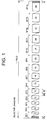
- FIG. 1 is a diagram showing an exemplary light emission driving sequence based on such a subfield method (refer to FIG. 14 of Japanese Patent Kokai No.2000-227778 (Patent Document 1) as an example).
- a field period is divided into fourteen subfields of SF1 to SF14. Only in the subfield SF1 locating first of those SF1 to SF14, all of the discharge cells of a PDP are initiated to be in a lighting mode (Rc). On the basis of each subfield SF1 to SF14, an input video signal is referred to set the corresponding discharge cells to an extinction mode (Wc), and only the discharge cells in the lighting mode are discharged for light emission for the duration allocated to the subfield (Ic).
- Wc extinction mode
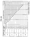
- FIG. 2 is a diagram showing an exemplary light emission driving pattern in a subfield period of each discharge cells to be driven based on such an light emission driving sequence (refer to FIG. 27 of Patent Document 1, for example).
- the discharge cells initiated to be in the lighting mode in the first subfield SF1 are set to the extinction mode as shown by black dots in any one of the subfields SF1 to Sf14. Once set as such, those are not put back to the lighting mode again.
- the discharge cells continuously discharge for light emission in the subfields as shown by white dots until set to the extinction mode.
- the fifteen light emission patterns of FIG. 2 vary in total light emission duration in a field period, representing fifteen intermediate luminance levels. That is, achieved thereby is intermediate luminance display of (N+1) tones (where N is the number of subfields).
- the problem with such a driving method is that the subfields as a result of field division are limited in number, causing shortage of the number of tones.
- the input video signal is subjected to a multi-grayscale process such as error diffusion and dithering.
- an input video signal is converted into pixel data on a pixel basis, for example pixel data of eight bits.
- pixel data for example pixel data of eight bits.
- six significant bits are regarded as display data, and the remaining two less-significant bits as error data.
- the error data of the pixel data derived for each pixel in a close range is assigned weights and added together, and the result derived thereby is reflected to the display data.
- the luminance of the less-significant two bits is represented in a pseudo manner by other pixels therearound, enabling representation of luminance tone equivalent to pixel data of eight bits using display data of only six bits.
- the error-diffused pixel data of six bits derived by such an error diffusion process is subjected to dithering.
- dithering a plurality of adjacent pixels are regarded as a pixel unit, and to the error-diffused pixel data corresponding to each pixel in the pixel unit, a dither coefficient is assigned.
- the dither coefficients vary in value, and after such assignment, the dither coefficients are added together.
- luminance representation so far required eight bits can be achieved only by four significant bits of the dither-added pixel data. Accordingly, four significant bits of the dither-added pixel data are extracted, and the extraction result is assigned to 15 light emission patterns of FIG. 2 as multi-grayscale pixel data PDs.
- the present invention is proposed for solving the above problems, and an object thereof is to provide a display panel drive capable of satisfactory image display with dither patterns suppressed.
- a first aspect of the present invention is directed to a display panel drive for tone-driving, responding to pixel data based on a video signal, a display panel in which a field display period of the video signal is constituted by a plurality of subfields, and pixel cells each carrying a pixel for n (where n is a natural number) display lines are arranged, the display panel drive comprising: a multi-grayscale means for deriving multi-grayscale pixel data by adding each different offset value to the pixel data corresponding to a display line group including [M ⁇ (k-1)+1]th display lines (where M is a natural number, and k is a natural number of n/M or smaller) of the display panel, a display line group including [M ⁇ (k-1)+2]th display lines thereof, a display line group including [M ⁇ (k-1)+3]th display lines thereof, ..., a display line group including [M ⁇ (k-1)+M]th display lines thereof; and an address
- a second aspect of the present invention is directed to a display panel drive for tone-driving, responding to pixel data based on a video signal, a display panel in which pixel cells each carrying a pixel for a plurality of display lines are arranged, the display panel drive comprising: a multi-grayscale means for deriving multi-grayscale pixel data by adding each different offset value to the pixel data each corresponding to m display lines belonging to a display line group including m (where m is a natural number of 2 or larger) display lines adjacent to one another; and an light emission driving means for emitting the pixel cells depending on the multi-grayscale pixel data by weighing the display line groups each differently in luminance.
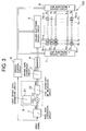
- FIG. 3 is a diagram showing the schematic structure of a plasma display device as a display device of the present invention.
- a PDP 100 being a plasma display panel includes a front substrate (not shown) serving as a display plane and a rear substrate (not shown) opposing to the front substrate with a discharge-gas-filled discharge space therebetween.
- the front substrate is formed with strip-shaped row electrodes X 1 to X n and Y 1 to Y n arranged alternately and parallel with one another.
- Formed on the rear substrate are strip-shaped column electrodes D 1 to D m intersected on the row electrodes X 1 to X n and Y 1 to Y n .
- each pair of row electrodes X and Y serves as a display line of the PDP 100, from the 1st line to the nth line.
- a discharge cell G serving as a pixel. That is, the PDP 100 includes (n ⁇ m) discharge cells G (1, 1) to G (n, m) formed in a matrix.
- a pixel data conversion circuit 1 converts an input video signal into pixel data PD on a pixel basis, for example pixel data of six bits. Then, the resulting data is supplied to a multi-grayscale processing circuit 2, which is constituted by a line offset data generation circuit 21, an adder 22, and a less-significant bit truncation circuit 23.
- the line offset data generation circuit 21 When the pixel data conversion circuit 1 outputs pixel data PD corresponding to the (4N-3)th display lines [N: natural number of (1/4) ⁇ n or smaller] of the PDP 100, the line offset data generation circuit 21 generates line offset data LD representing "10" (decimal numeral). Thus generated data is supplied to the adder 22. Similarly, when the pixel data conversion circuit 1 outputs pixel data PD corresponding to the (4N-2)th display lines, the line offset data generation circuit 21 generates line offset data LD representing "8" (decimal numeral) for supply to the adder 22.
- the line offset data generation circuit 21 When the pixel data conversion circuit 1 outputs pixel data PD corresponding to the (4N-1)th display lines, the line offset data generation circuit 21 generates line offset data LD representing "6" (decimal numeral) for supply to the adder 22. Further, when the pixel data conversion circuit 1 outputs pixel data PD corresponding to the (4N)th display lines, the line offset data generation circuit 21 generates line offset data LD representing "4" (decimal numeral) for supply to the adder 22.
- the adder 22 adds the corresponding line offset data LD.
- the resulting offset-added pixel data is then supplied to the less-significant bit truncation circuit 23.
- the less-significant bit truncation circuit 23 truncates three less-significant bits of the offset-added pixel data, and the remaining three significant bits are supplied to a driving data conversion circuit 3 as multi-grayscale pixel data MD.
- the driving data conversion circuit 3 converts thus provided multi-grayscale pixel data MD into pixel driving data GD of five bits in accordance with a data conversion table shown in FIG. 4. The resulting data is then supplied to memory 4.
- the memory 4 sequentially receives and stores the pixel driving data GD of five bits. Every time completing writing of pixel driving data GD 1,1 to GD n,m of an image frame (n lines ⁇ m columns), the memory 4 separates each of the pixel driving data GD 1,1 to GD n,m on a bit digit (1st to 5th bits) basis. Then, the memory 4 performs reading on a display line basis corresponding to subfields SF1 to SF4, which will be described later. The memory 4 then supplies, to a column electrode driving circuit 5, pixel driving data bits of thus read one display line (m bits) as pixel driving data bits DB1 to DB(m).
- the memory 4 reads only the 1st bit of the pixel driving data GD 1,1 to GD n , m for every display line. Thus read results are supplied to the column electrode driving circuit 5 as the pixel driving data bits DB1 to DB(m). Then, in subfields SF1 2 to SF2 1 , the memory 4 reads only the 2nd bit of the pixel driving data GD 1,1 to GD n,m for every display line, and thus read results are supplied to the column electrode driving circuit 5 as the pixel driving data bits DB1 to DB(m).
- the memory 4 reads only the 3rd bit of the pixel driving data GD 1,1 to GD n,m for every display line for supply to the column electrode . driving circuit 5 as the pixel driving data bits DB1 to DB(m). Then, in subfields SF3 2 to SF4 1 , the memory 4 reads only the 4th bit of the pixel driving data GD 1,1 to GD n,m for every display line for supply to the column electrode driving circuit 5 as the pixel driving data bits DB1 to DB(m).
- the memory 4 reads only the 5th bit of the pixel driving data GD 1,1 to GD n,m for every display line for supply to the column electrode driving circuit 5 as the pixel driving data bits DB1 to DB(m).
- a driving control circuit 6 supplies various timing signals for tone-driving the PDP 100 to the column electrode driving circuit 5, a row electrode Y driving circuit 7, and a row electrode X driving circuit 8.
- the display period of a field is divided into the subfields SF1 to SF4, and for each of the subfields, various driving processes are carried out as below.
- the subfields SF1 to SF4 are constituted by, respectively, four subfields of SF1 1 to SF1 4 , SF2 1 to SF2 4 , SF3 1 to SF3 4 , SF4 1 to SF4 4 as shown in FIG. 5.
- a reset process R every discharge cell of the PDP 100 is initiated to be in a lighting mode (state of predetermined wall charge being formed).
- the discharge cells are selectively shifted to be in an extinction mode (state of wall charge being eliminated) with respect to every display line depending on the pixel driving data.
- the sustain process I only the discharge cells in the lighting mode are discharged for light emission continuously over the period of "2".
- an address process W4 and the sustain process I are carried out. Specifically, in the address process W4, the discharge cells belonging to the (4N)th display lines are selectively shifted to the extinction mode depending on the pixel driving data. In the sustain process I, only the discharge cells in the lighting mode are discharged for light emission continuously over the period of "2".
- each of the subfields SF1 2 , SF2 2 , SF3 2 , and SF4 2 carried out are an address process W1 and the sustain process I.
- the address process W1 the discharge cells belonging to the (4N-3)th display lines are selectively shifted to the extinction mode depending on the pixel driving data.
- the sustain process I only the discharge cells in the lighting mode are discharged for light emission continuously over the period of "2".
- each of the subfields SF1 3 , SF2 3 , SF3 3 , and SF4 3 carried out are an address process W2 and the sustain process I.
- the address process W2 the discharge cells belonging to the (4N-2)th display lines are selectively shifted to the extinction mode depending on the pixel driving data.
- the sustain process I only the discharge cells in the lighting mode are discharged for light emission continuously over the period of "2".
- each of the subfields SF1 4 , SF2 4 , SF3 4 , and SF4 4 carried out are an address process W3 and the sustain process I.
- the address process W3 the discharge cells belonging to the (4N-1)th display lines are selectively shifted to the extinction mode depending on the pixel driving data.
- the sustain process I only the discharge cells in the lighting mode are discharged for light emission continuously over the period of "2".
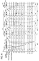
- FIG. 6 is a diagram showing various driving pulses to be applied to the PDP 100, and their application timings in accordance with such an light emission driving sequence.
- Such application is made by the column electrode driving circuit 5, the row electrode Y driving circuit 7, and the row electrode X driving circuit 8 responding to various timing signals provided by the driving control circuit 6.
- the various driving pulses to be applied to the PDP 100 and their application timings are all the same.
- the various driving pulses to be applied to the PDP 100 and their application timings are all the same.
- FIG. 6 shows only the subfield SF1 1 to the address process W4 in the subfield SF2 1 .
- the row electrode X driving circuit 8 First in the reset process R in the subfield SF1 1 , the row electrode X driving circuit 8 generates a negative reset pulse RP x showing mild falling edge change. Thus generated pulse is applied to the row electrodes X 1 to X n of the PDP 100.
- the row electrode Y driving circuit 7 At the same time as such a reset pulse RP x , the row electrode Y driving circuit 7 generates a positive reset pulse RP y showing mild rising edge change for application to the row electrodes Y 1 to Y n of the PDP 100.
- Such simultaneous application of the reset pulses RP x and RP y responsively causes reset discharge to occur to every discharge cell of the PDP 100, resultantly forming wall charge in each of the discharge cells. In this manner, all of the discharge cells are initiated to be in the lighting mode, being emissive state (light light emission responding to sustain discharge) in the sustain process I (described below).
- the row electrode Y driving circuit 7 sequentially applies a negative scanning pulse SP to the row electrodes Y 1 to Y n .
- the column electrode driving circuit 5 generates m pixel data pulses for a display line corresponding to the pixel driving data bits DB1 to DB(m) read from the memory 4.
- a pixel data pulse group DP consisted of thus generated m pixel data pulses is applied to the column electrodes D 1 to D m , respectively, in synchronization with the scanning pulse SP. That is, as shown in FIG.
- pixel data pulse groups DP 1 to DP n sequentially applied to the column electrodes D 1 to D m are pixel data pulse groups DP 1 to DP n corresponding to the 1st to nth display lines of the PDP 100, respectively.
- the pixel data pulse generated by the column electrode driving circuit 5 is high in voltage when the pixel driving data bit DB is in the logic level 1, and when in the logic level 0, the pixel data pulse will be low in voltage.
- erasure addressing discharge occurs only to the discharge cells locating at intersections of the display lines and the column electrodes.
- the display lines are those having applied with the scanning pulse SP
- the column electrodes are those having applied with the pixel data pulse of high voltage.
- all of the discharge cells of the PDP 100 are selectively put to cause erasure addressing discharge based on the pixel data.
- the discharge cells are each set to be in either the lighting mode or the extinction mode.
- the row electrode X driving circuit 8 and the row electrode Y driving circuit 7 alternately apply positive sustain pulses IP x and IP y repeatedly for a predetermined number of times to the row electrodes X 1 to X n and Y 1 to Y n as shown in FIG. 6.
- sustain discharge occurs only to the discharge cells with the wall charge remained therein, i.e., the discharge cells set in the lighting mode. Those discharge cells sustain the light emission state resulting from such sustain discharge.
- only the discharge cells sustaining the state of the lighting mode without erasure addressing discharge occurring in the address process W0 in the subfield SF1 1 emit in the sustain process I over the predetermined period of "2".
- the row electrode Y driving circuit 7 sequentially applies a negative scanning pulse SP to any row electrode Y belonging to the (4N-3)th display lines [N: 1 to (1/4) ⁇ n] of the PDP 100, i.e., the row electrodes Y 1 , Y 5 , Y 9 , ..., Y (n-3) ⁇
- the column electrode driving circuit 5 generates m pixel data pulses for a display line corresponding to the pixel driving data bits DB1 to DB(m) read from the memory 4.
- the pixel data pulse group DP consisted of the resulting m pixel data pulses is applied to the column electrodes D 1 to D m in synchronization with the scanning pulse SP.
- the column electrode driving circuit 5 sequentially applies the pixel data pulse groups DP 1 , DP 5 , DP 9 , ..., DP (n-3) corresponding to the (4N-3)th display lines to the column electrodes D 1 to D m as shown in FIG. 6.
- the pixel data pulse generated by the column electrode driving circuit 5 is high in voltage when the pixel driving data bit DB is in the logic level 1, and when in the logic level 0, the pixel data pulse will be low in voltage.
- erasure addressing discharge occurs only to the discharge cells locating at intersections of the display lines and the column electrodes.
- the display lines are those having applied with the scanning pulse SP
- the column electrodes are those having applied with the pixel data pulse of high voltage.
- the wall charge so far formed in the discharge cells is eliminated, and the resulting discharge cells shift into the extinction mode, being non-emissive state (light emission responding to sustain discharge) in the sustain process I.
- no such erasure addressing discharge occurs to the discharge cells having applied with the scanning pulse SP and with the pixel data pulse but of low voltage, and thus the mode immediately before (lighting or extinction mode) is sustained.
- the discharge cells belonging to the (4N-3)th display lines of the PDP 100 are selectively put to cause erasure addressing discharge based on the pixel data.
- the discharge cells are each set to be in either the lighting mode or the extinction mode.
- the row electrode X driving circuit 8 and the row electrode' Y driving circuit 7 alternately apply positive sustain pulses IP x and IP y repeatedly for a predetermined number of times to the row electrodes X 1 to X n and Y 1 to Y n as shown in FIG. 6.
- sustain discharge occurs only to the discharge cells with the wall charge remained therein, i.e., the discharge cells set in the lighting mode. Those discharge cells sustain the light emission state resulting from such sustain discharge.
- the row electrode Y driving circuit 7 sequentially applies a negative scanning pulse SP to any row electrode Y belonging to the (4N-2)th display lines [N: natural number of (1/4) ⁇ n or smaller] of the PDP 100, i.e., the row electrodes Y 2 , Y 6 , Y 10 , ..., Y (n-2) .
- the column electrode driving circuit 5 generates m pixel data pulses for a display line corresponding to the pixel driving data bits DB1 to DB(m) read from the memory 4.
- the pixel data pulse group DP consisted of the resulting m pixel data pulses is applied to the column electrodes D 1 to D m in synchronization with the scanning pulse SP.
- the column electrode driving circuit 5 sequentially applies the pixel data pulse groups DP 2 , DP 6 , DP 10 , ..., DP (n-2) corresponding to the (4N-2) th display lines to the column electrodes D 1 to D m as shown in FIG. 6.
- the pixel data pulse generated by the column electrode driving circuit 5 is high in voltage when the pixel driving data bit DB is in the logic level 1, and when in the logic level 0, the pixel data pulse will be low in voltage.
- erasure addressing discharge occurs only to the discharge cells locating at intersections of the display lines and the column electrodes.
- the display lines are those having applied with the scanning pulse SP
- the column electrodes are those having applied with the pixel data pulse of high voltage.
- the wall charge so far formed in the discharge cells is eliminated, and the resulting discharge cells shift into the extinction mode.
- no such erasure addressing discharge occurs to the discharge cells having applied with the scanning pulse SP and with the pixel data pulse but of low voltage, and thus the mode immediately before (lighting or extinction mode) is sustained.
- the discharge cells belonging to the (4N-2)th display lines of the PDP 100 are selectively put to cause erasure addressing discharge based on the pixel data.
- the discharge cells are each set to be in either the lighting mode or the extinction mode.
- the row electrode X driving circuit 8 and the row electrode Y driving circuit 7 alternately apply positive sustain pulses IP x and IP y repeatedly for a predetermined number of times to the row electrodes X 1 to X n and Y 1 to Y n as shown in FIG. 6.
- sustain discharge occurs only to the discharge cells with the wall charge remained therein, i.e., the discharge cells set in the lighting mode. Those discharge cells sustain the light emission state resulting from such sustain discharge.
- only the discharge cells sustaining the state of the lighting mode without erasure addressing discharge occurring in the address processes W0, W1, and W2 emit in the sustain process I over the predetermined period of "2".
- the row electrode Y driving circuit 7 sequentially applies a negative scanning pulse SP to any row electrode Y belonging to the (4N-1)th display lines [N: natural number of (1/4) ⁇ n or smaller] of the PDP 100, i.e., the row electrodes Y 3 , Y 7 , Y 11 , ... , Y (n-1) ⁇ During this time, the column electrode driving circuit 5 generates m pixel data pulses for a display line corresponding to the pixel driving data bits DB1 to DB(m) read from the memory 4.
- the pixel data pulse group DP consisted of the resulting m pixel data pulses is applied to the column electrodes D 1 to D m in synchronization with the scanning pulse SP.
- the column electrode driving circuit 5 sequentially applies the pixel data pulse groups DP 3 , DP 7 , DP 11 , ..., DP (n-1) corresponding to the (4N-1)th display lines to the column electrodes D 1 to D m as shown in FIG. 6.
- the pixel data pulse generated by the column electrode driving circuit 5 is high in voltage when the pixel driving data bit DB is in the logic level 1, and when in the logic level 0, the pixel data pulse will be low in voltage.
- erasure addressing discharge occurs only to the discharge cells locating at intersections of the display lines and the column electrodes.
- the display lines are those having applied with the scanning pulse SP
- the column electrodes are those having applied with the pixel data pulse of high voltage.
- the wall charge so far formed in the discharge cells is eliminated, and the resulting discharge cells shift into the extinction mode.
- no such erasure addressing discharge occurs to the discharge cells having , applied with the scanning pulse SP and with the pixel data pulse but of low voltage, and thus the mode immediately before (lighting or extinction mode) is sustained.
- the discharge cells belonging to the (4N-1)th display lines of the PDP 100 are selectively put to cause erasure addressing discharge based on the pixel data.
- the discharge cells are each set to be in either the lighting mode or the extinction mode.
- the row electrode X driving circuit 8 and the row electrode Y driving circuit 7 alternately apply positive sustain pulses IP x and IP y repeatedly for a predetermined number of times to the row electrodes X 1 to X n and Y 1 to Y n as shown in FIG. 6.
- sustain discharge occurs only to the discharge cells with the wall charge remained therein, i.e., the discharge cells set in the lighting mode.
- Those discharge cells sustain the light emission state resulting from such sustain discharge.
- only the discharge cells sustaining the state of the lighting mode without erasure addressing discharge occurring in the address processes W0, W1, W2, and W3 emit in the sustain process I over the predetermined period of "2".
- the row electrode Y driving circuit 7 sequentially applies a negative scanning pulse SP to any row electrode Y belonging to the (4N)th display lines [N: 1 to (1/4) ⁇ n] of the PDP 100, i.e., the row electrodes Y 4 , Y 8 , Y 12 , ..., Y n .
- the column electrode driving circuit 5 generates m pixel data pulses for a display line corresponding to the pixel driving data bits DB1 to DB(m) read from the memory 4.
- the pixel data pulse group DP consisted of the resulting m pixel data pulses is applied to the column electrodes D 1 to D m in synchronization with the scanning pulse SP.
- the column electrode driving circuit 5 sequentially applies the pixel data pulse groups DP 4 , DP 8 , DP 12 , ..., DP n corresponding to the (4N)th display lines to the column electrodes D 1 to D m as shown in FIG. 6.
- the pixel data pulse generated by the column electrode driving circuit 5 is high in voltage when the pixel driving data bit DB is in the logic level 1, and when in the logic level 0, the pixel data pulse will be low in voltage.
- erasure addressing discharge occurs only to the discharge cells locating at intersections of the display lines and the column electrodes.
- the display lines are those having applied with the scanning pulse SP
- the column electrodes are those having applied with the pixel data pulse of high voltage.
- the wall charge so far formed in the discharge cells is eliminated, and the resulting discharge cells shift into the extinction mode.
- no such erasure addressing discharge occurs to the discharge cells having applied with the scanning pulse SP and with the pixel data pulse but of low voltage, and thus the mode immediately before (lighting or extinction mode) is sustained.
- the discharge cells belonging to the (4N)th display lines of the PDP 100 are selectively put to cause erasure addressing discharge based on the pixel data.
- the discharge cells are each set to be in either the lighting mode or the extinction mode.
- the row electrode X driving circuit 8 and the row electrode Y driving circuit 7 alternately apply positive sustain pulses IP x and IP y repeatedly for a predetermined number of times to the row electrodes X 1 to X n and Y 1 to Y n .
- sustain discharge occurs only to the discharge cells with the wall charge remained therein, i.e., the discharge cells set in the lighting mode. Those discharge cells sustain the light emission state resulting from such sustain discharge.
- only the discharge cells sustaining the state of the lighting mode without erasure addressing discharge occurring in the address processes W0, W1, W2, W3, and W4 emit in the sustain process I over the predetermined period of "2".
- sustain discharge light emission (indicated by white dots) occurs continually in the sustain process I in the respective subfields. During this time, perceived is the intermediate luminance corresponding to the total light emission duration in one field period caused by such sustain discharge light emission.
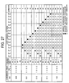
- the discharge cells belonging to four display lines vertically adjacent to one another in the screen of the PDP 100 i.e., for each of these discharge cells belonging to (4N-3)th display lines, discharge cells belonging to (4N-2)th display lines, discharge cells belonging to (4N-1)th display lines, and discharge cells belonging to (4N)th display lines, the total light emission duration differs in each field period responding to the driving based on the pixel driving data GD.
- the discharge cells belonging to the (4N-3)th display lines i.e., 1st, 5th, 9th, ..., and (n-3)th display lines, are put to cause sustain discharge for light emission in the sustain process I of the subfields SF1 1 to SF1 4 , and SF2 1 as indicated by white dots.
- the discharge cells belonging to the (4N-2)th display lines i.e., 2nd, 6th, 10th, ..., and (n-2)th display lines, are put to cause sustain discharge for light emission in the sustain process I of the subfields SF1 1 to SF1 4 , SF2 1 , and SF2 2 .
- the discharge cells belonging to the (4N-1)th display lines i.e., 3rd, 7th, 11th, ..., and (n-1)th display lines, are put to cause sustain discharge for light emission in the sustain process I of the subfields SF1 1 to SF1 4 , and SF2 1 to SF2 3 .
- the discharge cells belonging to the (4N)th display lines i.e., 4th, 8th, 12th, ..., and nth display lines, are put to cause sustain discharge for light emission in the sustain process I of the subfields SF1 1 to SF1 4 , and SF2 1 to SF2 4 .
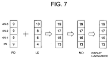
- the total light emission duration in one field period caused by sustain discharge light emission occurred responding to the pixel driving data GD of [01000] as shown in FIG. 4 will be as follows:
- the pixel data PD is added with the line offset data LD.
- line offset data LD as "10" to pixel data PD corresponding to (4N-3)th display lines, "8” to pixel data PD corresponding to (4N-2)th display lines, "6” to pixel data PD corresponding to (4N-1)th display lines, and "4" to pixel data PD corresponding to (4N)th display lines.
- pixel data PD (1,1) , PD (2,1) , PD (3,1) , and PD (4,1) corresponding, respectively, to discharge cells G (1,1) , G (2,1) , G (3,1) , and G (4,1) vertically adjacent to one another in the screen of the PDP 100 are all six-bit data [001001] representing "9" (decimal numeral).
- line offset data LD of "10", “8", "4", and "2" as shown in FIG.
- the discharge cell G (1,1) belonging to the (4N-3)th display lines is put to cause sustain discharge for light emission in the sustain processes I in the subfields SF1 1 to SF1 4 , and SF2 1 as indicated by the white dots of FIG. 4.
- the discharge cell G (2,1) belonging to the (4N-2)th display lines is put to cause sustain discharge for light emission in the sustain processes I in the subfields SF1 1 to SF1 4 , SF2 1 , and SF2 2 .
- the discharge cell G (3,1) belonging to the (4N-1)th display lines is put to cause sustain discharge for light emission in the sustain processes I in the subfields SF1 1 to SF1 3 as indicated by the white dots of FIG. 4.
- perceived is the light emission luminance of "6”.
- the discharge cell G (4,1) belonging to the (4N)th display lines is put to cause sustain discharge for light emission in the sustain processes I in the subfields SF1 1 to SF1 4 as indicated by the white dots of FIG. 4.
- the four discharge cells G (1,1)' G (2,1) , G (3,1) , and G (4,1) vertically adjacent to one another in the screen of the PDP 100 each emit representing as follows:
- the line offset data LD being "10", “8", “6”, and "4" are assigned, for addition, to pixel data PD corresponding to the (4N-3)th display lines, the (4N-2)th display lines, the (4N-1)th display lines, and the (4N)th display lines.
- the light emission driving sequence to be adopted is changed for the 1st to 4th fields. Specifically, in the 1st field, executed is driving in accordance with such an light emission driving sequence as shown in FIG. 5. In the 2nd to 4th fields, the address process is changed in execution order in the subfields SF1 2 to SF1 4 , SF2 1 to SF2 4 , SF3 1 to SF3 4 , and SF4 1 to SF 4 4 shown in Fig. 5.
- executed in the subfield SF1 1 is the address process W0 to every display line similarly to the light emission driving sequence shown in FIG. 5.
- executed is the address process W3 to the (4N-1)th display lines
- executed is the address process W4 to the (4N)th display lines
- executed is the address process W1 to the (4N-3)th display lines
- executed is the address process W2 to the (4N-2)th display lines.
- executed in the subfield SF1 1 is the address process W0 to every display line similarly to the light emission driving sequence shown in FIG. 5.
- executed in the subfields SF2 1 , SF3 1 , and SF4 1 is the address process W2 to the (4N-2)th display lines
- executed in the subfields SF1 2 , SF2 2 , SF 3 2 , and SF4 2 executed is the address process W3 to the (4N-1)th display lines
- executed in the subfields SF1 3 , SF2 3 , SF3 3 , and SF4 3 executed is the address process W4 to the (4N)th display lines
- executed in the subfields SF1 4 , SF2 4 , SF3 4 , and SF4 4 executed is the address process W1 to the (4N-3)th display lines.
- executed in the subfield SF1 1 is the address process W0 to every display line similarly to the light emission driving sequence shown in FIG. 5.
- executed in the subfields SF2 1 , SF3 1 , and SF4 1 is the address process W1 to the (4N-3)th display lines
- executed in the subfields SF1 2 , SF2 2 , SF3 2 , and SF4 2 executed is the address process W2 to the (4N-2)th display lines
- executed in the subfields SF1 3 , SF2 3 , SF3 3 , and SF4 3 executed is the address process W3 to the (4N-1)th display lines
- executed in the subfields SF1 4 , SF2 4 , SF3 4 , and SF4 4 executed is the address process W4 to the (4N)th display lines.
- the (4N-3)th display lines, the (4N-2)th display lines, the (4N-1)th display lines, and the (4N)th display lines vary in luminance levels of 4 stages on a field basis as shown in FIG. 12. Accordingly, this considerably reduces the dithering pattern from occurring.
- FIG. 13 is a diagram showing the schematic structure of a plasma display device according to another embodiment of the present invention.
- the PDP 100 being a plasma display panel includes a front substrate (not shown) serving as a display plane and a rear substrate (not shown) opposing to the front substrate with a discharge-gas-filled discharge space therebetween.
- the front substrate is formed with strip-shaped row electrodes X 1 to X n and Y 1 to Y n arranged alternately and parallel with one another.
- Formed on the rear substrate are strip-shaped column electrodes D 1 to D m intersected on the row electrodes X 1 to X n and Y 1 to Y n .
- each pair of row electrodes X and Y serves as a display line of .
- the PDP 100 from 1st to nth. At an intersection part (discharge space included) of a pair of row electrode and column electrode, formed is a discharge cell G serving as a pixel. That is, the PDP 100 includes (n x m) discharge cells G (1,1) to G (n , m ) formed in a matrix.
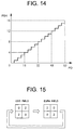
- a pixel data conversion circuit 10 converts an input video signal into pixel data PD on a pixel basis, for example pixel data of six bits. Then, the resulting data is supplied to a first data conversion circuit 11, which converts the pixel data PD into first conversion pixel data PD1 of five bits in accordance with such conversion characteristics as shown in FIG. 14. The resulting data is supplied to a multi-grayscale processing circuit 20. Note here that, in FIG. 14, the pixel data PD and the first conversion pixel data PD1 are each represented by decimal numeral.
- the multi-grayscale processing circuit 20 is constituted by an adder 200, a line offset data generation circuit 210, a dither matrix circuit 220, and a less-significant bit truncation circuit 230.
- the line offset data generation circuit 210 When the first data conversion circuit 11 outputs first conversion pixel data PD1 corresponding to the (4N-3)th display lines [N: natural number of (1/4) ⁇ n or smaller] of the PDP 100, the line offset data generation circuit 210 generates line offset data LD representing "3" (decimal numeral). Thus generated data is supplied to the adder 200. Similarly, when the first data conversion circuit 11 output's first conversion pixel data PD1 corresponding to the (4N-2)th display lines, the line offset data generation circuit 210 generates line offset data LD representing "2" (decimal numeral) for supply to the adder 200.
- the line offset data generation circuit 210 When the first data conversion circuit 11 outputs first conversion pixel data PD1 corresponding to the (4N-1)th display lines, the line offset data generation circuit 210 generates line offset data LD representing "1" (decimal numeral) for supply to the adder 200. Further, when the first data conversion circuit 11 outputs first conversion pixel data PD1 corresponding to the (4N)th display lines, the line offset data generation circuit 210 generates line offset data LD representing "0" (decimal numeral) for supply to the adder 200.
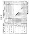
- the dither matrix circuit 220 On the basis of each pixel group constituted by four pixels adjacent to one another in the vertical and lateral directions of the screen, the dither matrix circuit 220 generates a dither coefficient of "0" or "2" (decimal numeral) as shown in FIG. 15 for each pixel in the pixel group. The resulting dither coefficients are provided to the adder 200.
- the dither matrix circuit 220 changes such dither coefficient assignment for each pixel in the pixel group on a field basis as shown in FIG. 15.
- the adder 200 adds the dither coefficient to the first conversion pixel data PD1 of five bits provided by the first data conversion circuit 11, deriving dither-added pixel data. To the dither-added pixel data, the adder 200 adds the line offset data LD for supply to the less-significant bit truncation circuit 230.
- the less-significant bit truncation circuit 230 truncates two less-significant bits of the dither-added pixel data having added with the line offset data LD, and the remaining three significant bits are provided to a driving data conversion circuit 30 as multi-grayscale pixel data MD.
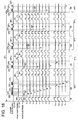
- the driving data conversion circuit 30 converts the multi-grayscale pixel data MD into pixel driving data GD of five bits in accordance with a data conversion table shown in FIG. 16. The resulting data is supplied to memory 40.
- the memory 40 sequentially receives and stores the pixel driving data GD of five bits. Every time completing writing of pixel driving data GD 1,1 to GD n,m of an image frame (n lines ⁇ m columns), the memory 40 separates each of the pixel driving data GD 1,1 to GD n,m on a bit digit (1st to 5th bits) basis. Then, the memory 40 performs reading on a display line basis corresponding to subfields SF1 to SF4, which will be described later. The memory 40 then supplies, to a column electrode driving circuit 50, the pixel driving data bits of thus read one display line (m bits) as pixel driving data bits DB1 to DB(m).
- the memory 40 reads only the 1st bit of the pixel driving data GD 1,1 to GD n,m , for every display line. Thus read results are supplied to the column electrode driving circuit 50 as pixel driving data bits DB1 to DB(m). Then, in subfields SF1 2 to SF2 1 , the memory 40 reads only the 2nd bit of the pixel driving data GD 1,1 to GD n,m for every display line, and thus read results are supplied to the column electrode driving circuit 50 as the pixel driving data bits DB1 to DB(m).
- the memory 40 reads only the 3rd bit of the pixel driving data GD 1,1 to GD n,m for every display line, and thus read results are supplied to the column electrode driving circuit 50 as the pixel driving data bits DB1 to DB(m). Then, in subfields SF3 2 to SF4 1 , the memory 40 reads only the 4th bit of the pixel driving data GD 1,1 to GD n,m for every display line, and thus read results are supplied to the column electrode driving circuit 50 as the pixel driving data bits DB1 to DB (m) .
- the memory 40 reads only the 5th bit of the pixel driving data GD 1,1 to GD n,m for every display line, and thus read results are supplied to the column electrode driving circuit 50 as the pixel driving data bits DB1 to DB(m).
- a driving control circuit 60 supplies various timing signals for tone-driving the PDP 100 to the column electrode driving circuit 50, a row electrode Y driving circuit 70, and a row electrode X driving circuit 80.
- the display period of a field is divided into the subfields SF1 to SF4, and for each of the subfields, various driving processes as below are carried out.
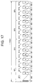
- the subfields SF1 to SF4 are constituted by, respectively, four subfields of SF1 1 to SF1 4 , SF2 1 to SF2 4 , SF3 1 to SF3 4 , SF4 1 to SF4 4 as shown in FIG. 17.
- a reset process R every discharge cell of the PDP 100 is initiated to be in a lighting mode (state of predetermined wall charge being formed).
- the discharge cells are selectively shifted to be in an extinction mode (state of wall charge being eliminated) with respect to every display line depending on the pixel driving data.
- the sustain process I only the discharge cells in the lighting mode are discharged for light emission continuously over the period of "6".
- an address process W4 and the sustain process I are carried out. Specifically, in the address process W4, the discharge cells belonging to the (4N)th display lines are selectively shifted to the extinction mode depending on the pixel driving data. In the sustain process I, only the discharge cells in the lighting mode are discharged for light emission continuously over the period of "4".
- each of the subfields SF1 2 , SF2 2 , SF3 2 , and SF4 2 carried out are an address process W1 and the sustain process I.
- the address process W1 the discharge cells belonging to the (4N-3)th display lines are selectively shifted to the extinction mode depending on the pixel driving data.
- the sustain process I only the discharge cells in the lighting mode are discharged for light emission continuously over the period of "4".
- each of the subfields SF1 3 , SF2 3 , SF3 3 , and SF4 3 carried out are an address process W2 and the sustain process I.
- the address process W2 the discharge cells belonging to the (4N-2)th display lines are selectively shifted to the extinction mode depending on the pixel driving data.
- the sustain process I only the discharge cells in the lighting mode are discharged for light emission continuously over the period of "4".
- each of the subfields SF1 4 , SF2 4 , SF3 4 , and SF4 4 carried out are an address process W3 and the sustain process I.
- the address process W3 the discharge cells belonging to the (4N-1)th display lines are selectively shifted to the extinction mode depending on the pixel driving data.
- the sustain process I only the discharge cells in the lighting mode are discharged for light emission continuously over the period of "4".
- FIG. 18 is a diagram showing various driving pulses to be applied to the PDP 100, and their application timings in accordance with such an light emission driving sequence.
- Such application is made by the column electrode driving circuit 50, the row electrode Y driving circuit 70, and the row electrode X driving circuit 80.
- the various driving pulses to be applied to the PDP 100 and their application timings are all the same.
- the various driving pulses to be applied to the PDP 100 and their application timings are all the same.
- FIG. 18 shows only the subfield SF1 1 to the address process W4 in the subfield SF2 1 .
- the row electrode X driving circuit 80 First in the reset process R in the subfield SF1 1 , the row electrode X driving circuit 80 generates a negative reset pulse RP x showing mild falling edge change. Thus generated pulse is applied to the row electrodes X 1 to X n of the PDP 100.
- the row electrode Y driving circuit 70 At the same time as such a reset pulse RP x , the row electrode Y driving circuit 70 generates a positive reset pulse RP y showing mild rising edge change for application to the row electrodes Y 1 to Y n of the PDP 100.
- Such simultaneous application of the reset pulses RP x and RP y responsively causes reset discharge to occur to every discharge cell of the PDP 100, resultantly forming wall charge in each of the discharge cells. In this manner, all of the discharge cells are initiated to be in the lighting mode, being emissive state (light emission responding to sustain discharge) in the sustain process I (described below).
- the row electrode Y driving circuit 70 sequentially applies a negative scanning pulse SP to the row electrodes Y 1 to Y n .
- the column electrode driving circuit 50 generates m pixel data pulses for a display line corresponding to pixel driving data bits DB1 to DB(m) read from the memory 40.
- a pixel data pulse group DP consisted of thus generated m pixel data pulses is applied to the column electrodes D 1 to D m , respectively, in synchronization with the scanning pulse SP. That is, as shown in FIG.
- pixel data pulse groups DP 1 to DP n sequentially applied to the column electrodes D 1 to D m are pixel data pulse groups DP 1 to DP n corresponding to the 1st to nth display lines of the PDP 100, respectively.
- the pixel data pulse generated by the column electrode driving circuit 50 is high in voltage when the pixel driving data bit DB is in the logic level 1, and when in the logic level 0, the pixel data pulse will be low in voltage.
- erasure addressing discharge occurs only to the discharge cells locating at intersections of the display lines and the column electrodes.
- the display lines are those having applied with the scanning pulse SP
- the column electrodes are those having applied with the pixel data pulse of high voltage.
- all of the discharge cells of the PDP 100 are selectively put to cause erasure addressing discharge based on the pixel data.
- the discharge cells are each set to be in either the lighting mode or the extinction mode.
- the row electrode X driving circuit 80 and the row electrode Y driving circuit 70 alternately apply positive sustain pulses IP x and IP y repeatedly for a predetermined number of times to the row electrodes X 1 to X n and Y 1 to Y n as shown in FIG. 18.
- sustain discharge occurs only to the discharge cells with the wall charge remained therein, i.e., the discharge cells set to be in the lighting mode.
- Those discharge cells sustain the light emission state resulting from such sustain discharge.
- only the discharge cells sustaining the state of the lighting mode without erasure addressing discharge occurring in the address process W0 in the subfield SF1 1 emit in the sustain process I over the predetermined period of "6".
- the row electrode Y driving circuit 70 sequentially applies'a negative scanning pulse SP to any row electrode Y belonging to the (4N-3)th display lines [N: 1 to (1/4) , ⁇ n] of the PDP 100, i.e., the row electrodes Y 1 , Y 5 , Y 9 , ..., Y (n-3) .
- the column electrode driving circuit 50 generates m pixel data pulses for a display line corresponding to the pixel driving data bits DB1 to DB(m) read from the memory 40.
- the pixel data pulse group DP consisted of the resulting m pixel data pulses is applied to the column electrodes D 1 to D m in synchronization with the scanning pulse SP.
- the column electrode driving circuit 50 sequentially applies the pixel data pulse groups DP 1 , DP 5 , DP 9 , ..., DP (n-3) corresponding to the (4N-3)th display lines to the column electrodes D 1 to D m as shown in FIG. 18.
- the pixel data pulse generated by the column electrode driving circuit 50 is high in voltage when the pixel driving data bit DB is in the logic level 1, and when in the logic level 0, the pixel data pulse will be low in voltage.
- erasure addressing discharge occurs only to the discharge cells locating at intersections of the display lines and the column electrodes.
- the display lines are those having applied with the scanning pulse SP
- the column electrodes are those having applied with the pixel data pulse of high voltage.
- the wall charge so far formed in the discharge cells is eliminated, and the resulting discharge cells shift into the extinction mode, being non-emissive state (light emission responding to sustain discharge) in the sustain process I (described below).
- no such erasure addressing discharge occurs to the discharge cells having applied with the scanning pulse SP and with the pixel data pulse but of low voltage, and thus the mode immediately before (lighting or extinction mode) is sustained.
- the discharge cells belonging to the (4N-3)th display lines of the PDP 100 are selectively put to cause erasure addressing discharge based on the pixel data.
- the discharge cells are each set to be in either the lighting mode or the extinction mode.
- the row electrode X driving circuit 80 and the row electrode Y driving circuit 70 alternately apply positive sustain pulses IP x and IP y repeatedly for a predetermined number of times to the row electrodes X 1 to X n and Y 1 to Y n as shown in FIG. 18.
- sustain discharge occurs only to the discharge cells with the wall charge remained therein, i.e., the discharge cells set in the lighting mode.
- Those discharge cells sustain the light emission state resulting , from such sustain discharge.
- only the discharge cells sustaining the state of the lighting mode without erasure addressing discharge occurring in the address processes W0 and W1 emit in the sustain process I over the predetermined period of "4".
- the row electrode Y driving circuit 70 sequentially applies a negative scanning pulse SP to any row electrode Y belonging to the (4N-2)th display lines [N: 1 to (1/4) n] of the PDP 100, i . e . , the row electrodes Y 2 , Y 6 , Y 10 , ..., Y (n-2) .
- the column electrode driving circuit 50 generates m pixel data pulses for a display line corresponding to the pixel driving data bits DB1 to DB(m) read from the memory 40.
- the pixel data pulse group DP consisted of the , resulting m pixel data pulses is applied to the column electrodes D 1 to D m in synchronization with the scanning pulse SP.
- the column electrode driving circuit 50 sequentially applies the pixel data pulse groups DP 2 , DP 6 , DP 10 , ..., DP (n-2) corresponding to the (4N-2)th display lines to the column electrodes D 1 to D m as shown in FIG. 18.
- the pixel data pulse generated by the column electrode driving circuit 50 is high in voltage when the pixel driving data bit DB is in the logic level 1, and when in the logic level 0, the pixel data pulse will be low in voltage.
- erasure addressing discharge occurs only to the discharge cells locating at intersections of the display lines and the column electrodes.
- the display lines are those having applied with the scanning pulse SP
- the column electrodes are those having applied with the pixel data pulse of high voltage.
- the wall charge so far formed in the discharge cells is eliminated, and the resulting discharge cells shift into the extinction mode.
- no such erasure addressing discharge occurs to the discharge cells having applied with' the scanning pulse SP and with the pixel data pulse but of low voltage, and thus the mode immediately before (lighting or extinction mode) is sustained.
- the discharge cells belonging to the (4N-2)th display lines of the PDP 100 are selectively put to cause erasure addressing discharge based on the pixel data.
- the discharge cells are each set to be in either the lighting mode or the extinction mode.
- the row electrode X driving circuit 80 and the row electrode Y driving circuit 70 alternately apply positive sustain pulses IP x and IP y repeatedly for a predetermined number of times to the row electrodes X 1 to X n and Y 1 to Y n as shown in FIG. 18.
- sustain discharge occurs only to the discharge cells with the wall charge remained therein, i.e., the discharge cells set in the lighting mode. Those discharge cells sustain the light emission state resulting from such sustain discharge.
- only the discharge cells sustaining the state of the lighting mode without erasure addressing discharge occurring in the address processes W0, W1, and W2 emit in the sustain process I over the predetermined period of "4".
- the row electrode Y driving circuit 70 sequentially applies a negative scanning pulse SP to any row electrode Y belonging to the (4N-1)th display lines [N: 1 to (1/4) ⁇ n] of the PDP 100, i . e . , the row electrodes Y 3 , Y 7 , Y 11 , ..., Y (n-1) .
- the column electrode driving circuit 50 generates m pixel data pulses for a display line corresponding to the pixel driving data bits DB1 to DB(m) read from the memory 40.
- the pixel data pulse group DP consisted of the resulting m pixel data pulses is applied to the column electrodes D 1 to D m in synchronization with the scanning pulse SP.
- the column electrode driving circuit 50 sequentially applies the pixel data pulse groups DP 3 , DP 7 , DP 11 , ..., DP (n-1) corresponding to the (4N-1)th display lines to the column electrodes D 1 to D m in as shown in FIG. 18.
- the pixel data pulse generated by the column electrode driving circuit 50 is high in voltage when the pixel driving data bit DB is in the logic level 1, and when in the logic level 0, the pixel data pulse will be low in voltage.
- erasure addressing discharge occurs only to the discharge cells locating at intersections of the display lines and the column electrodes.
- the display lines are those having applied with the scanning pulse SP
- the column electrodes are those having applied with the pixel data pulse of high voltage.
- the wall charge so far formed in the discharge cells is eliminated, and the resulting discharge cells shift into the extinction mode.
- no such erasure addressing discharge occurs to the discharge cells having applied with the scanning pulse SP and with the pixel data pulse but of low voltage, and thus the mode immediately before (lighting or extinction mode) is sustained.
- the discharge cells belonging to the (4N-1)th display lines of the PDP 100 are selectively put to cause erasure addressing discharge based on the pixel data.
- the discharge cells are each set to be in either the lighting mode or the extinction mode.
- the row electrode X driving circuit 80 and the row electrode Y driving circuit 70 alternately apply positive sustain pulses IP x and IP y repeatedly for a predetermined number of times to the row electrodes X 1 to X n and Y 1 to Y n as shown in FIG. 18.
- sustain discharge occurs only to the discharge cells with the wall charge remained therein, i.e., the discharge cells set in the lighting mode. Those discharge cells sustain the light emission state resulting from such sustain discharge.
- only the discharge cells sustaining the state of the lighting mode without erasure addressing discharge occurring in the address processes W0, W1, W2, and W3 emit in the sustain process I over the predetermined period of "4".
- the row electrode Y driving circuit 70 sequentially applies a negative scanning pulse SP to any row electrode Y belonging to the (4N)th display lines [N: 1 to (1/4) ⁇ n] of the PDP 100, i.e., the row electrodes Y 4 , Y 8 , Y 12 , ..., Y n .
- the column electrode driving circuit 50 generates m pixel data pulses for a display line corresponding to the pixel driving data bits DB1 to DB(m) read from the memory 40.
- the pixel data pulse group DP consisted of the resulting m pixel data pulses is applied to the column electrodes D 1 to D m in synchronization with the scanning pulse SP.
- the column electrode driving circuit 50 sequentially applies the pixel data pulse groups DP 4 , DP 8 , DP 12 , ..., DP n corresponding to the (4N)th display lines to the column electrodes D 1 to D m as shown in FIG. 18.
- the pixel data pulse generated by the column electrode driving circuit 50 is high in voltage when the pixel driving data bit DB is in the logic level 1, and when in the logic level 0, the pixel data pulse will be low in voltage.
- erasure addressing discharge occurs only to the discharge cells locating at intersections of the display lines and the column electrodes.
- the display lines are those having applied with the scanning pulse SP
- the column electrodes are those having applied with the pixel data pulse of high voltage.
- the wall charge so far formed in the discharge cells is eliminated, and the resulting discharge cells shift into the extinction mode.
- no such erasure addressing discharge occurs to the discharge cells having applied with the scanning pulse SP and with the pixel data pulse but of low voltage, and thus the mode immediately before (lighting or extinction mode) is sustained.
- the discharge cells belonging to the (4N)th display lines of the PDP 100 are selectively put to cause erasure addressing discharge based on the pixel data.
- the discharge cells are each set to be in either the lighting mode or the extinction mode.
- the row electrode X driving circuit 80 and the row electrode Y driving circuit 70 alternately apply positive sustain pulses IP x and IP y repeatedly for a predetermined number of times to the row electrodes X 1 to X n and Y 1 to Y n .
- sustain discharge occurs only to the discharge cells with the wall charge remained therein, i.e., the discharge cells set in the lighting mode. Those discharge cells sustain the light emission state resulting from such sustain discharge.
- only the discharge cells sustaining the state of the lighting mode without erasure addressing discharge occurring in the address processes W0, W1, W2, W3, and W4 emit in the sustain process I over the predetermined period of "4".
- sustain discharge light emission (indicated by white dots) occurs continually in the sustain process I in the respective subfields. During this time, perceived is the intermediate luminance corresponding to the total light emission duration in one field period caused by such sustain discharge light emission.
- the discharge cells belonging to four display lines vertically adjacent to one another in the screen of the PDP 100 i.e., for each of these discharge cells belonging to (4N-3)th display lines, discharge cells belonging to (4N-2)th display lines, discharge cells belonging to (4N-1)th display lines, and discharge cells belonging to (4N)th display lines, the total light emission duration differs in each field period responding to the driving according to the pixel driving data GD.
- the discharge cells belonging to the (4N-3)th display lines i.e., 1st, 5th, 9th, ..., and (n-3)th display lines, are put to cause sustain discharge for light emission in the sustain processes I of the subfields SF1 1 to SF1 4 , and SF2 1 as indicated by white dots.
- the discharge cells belonging to the (4N-2)th display lines i.e., 2nd, 6th, 10th, ..., and (n-2)th display lines, are put to cause sustain discharge for light emission in the sustain processes I of the subfields SF1 1 to SF1 4 , SF2 1 , and SF2 2 .
- the discharge cells belonging to the (4N-1)th display lines i.e., 3rd, 7th, 11th, ..., and (n-1)th display lines, are put to cause sustain discharge for light emission in the sustain processes I of the subfields SF1 1 to SF1 4 , and SF2 1 to SF2 3 .
- the discharge cells belonging to the (4N)th display lines i.e., 4th, 8th, 12th, ..., and nth display lines, are put to cause sustain discharge for light emission in the sustain processes I of the subfields SF1 1 to SF1 4 , and SF2 1 to SF2 4 .
- the total light emission duration in one field period caused by sustain discharge light emission occurred responding to the pixel driving data GD of [00100] will be as follows, as shown in FIG. 16, discharge cells belonging to (4N-3)th display lines: "22", discharge cells belonging to (4N-2)th display lines: “26", discharge cells belonging to (4N-1)th display lines: "30”, and discharge cells belonging to (4N)th display lines: "34".
- the total light emission duration in one field period caused by sustain discharge light emission occurred responding to the pixel driving data GD of [01000] will be as follows, as shown in FIG. 16, discharge cells belonging to (4N-3)th display lines: “6", discharge cells belonging to (4N-2)th display lines: “10", discharge cells belonging to (4N-1)th display lines: “14”, and discharge cells belonging to (4N)th display lines: "18".
- pixel data PD corresponding, respectively, to discharge cells G (1,1) , G (2,1 ), G (3,1) , and G (4,1) vertically adjacent to one another in the screen of the PDP 100, and discharge cells G (1,2) , G (2,2) , G (3,2) , G (4,2) locating thereright all are six-bit data representing "32" (decimal numeral) as shown in FIG. 19.
- the pixel data PD representing "32" is converted into first conversion pixel data PD1 of five bits representing "8" by the first data conversion circuit 11 with such conversion characteristics as shown in FIG. 14.
- the discharge cell G (1,1) belonging to the (4N-3)th display lines is put to cause sustain discharge for light emission in the sustain processes I in the subfields SF1 1 to SF1 4 , and SF2 1 as indicated by the white dot of FIG. 16.
- the discharge cell G (2,1) belonging to the (4N-2)th display lines is put to cause sustain discharge for light emission in the sustain processes I in the subfields SF1 1 to SF1 4 , SF2 1 to SF2 4 , SF3 1 , and SF3 2 .
- the discharge cell G (3,1) belonging to the (4N-1)th display lines is put to cause sustain discharge for light emission in the sustain processes I in the subfields SF1 1 to SF1 4 , and SF2 1 to SF2 3 as indicated by the white dot of FIG. 16.
- the discharge cell G (4,1) belonging to the (4N)th display lines is put to cause sustain discharge for light emission in the sustain processes I in the subfields SF1 1 to SF1 4 , and SF2 1 to SF2 4 as indicated by the white dot of FIG. 16.
- the discharge cell G (1,2) belonging to the (4N-3)th display lines is put to cause sustain discharge for light emission in the sustain processes I in the subfields SF1 1 to SF1 4 , SF2 1 to SF2 4 and SF3 1 as indicated by the white dot of FIG. 16.
- the discharge cell G (2,2) belonging to the (4N-2)th display lines is put to cause sustain discharge for light emission in the sustain processes I in the subfields SF1 1 to SF1 4 , and SF2 1 to SF2 4 .
- the discharge cell G (3,2) belonging to the (4N-1)th display lines is put to cause sustain discharge for light emission in the sustain processes I in the subfields SF1 1 to SF1 4 , and SF2 1 to SF2 3 as indicated by the white dot of FIG. 16.
- the discharge cell G (4,2) belonging to the (4N)th display lines is put to cause sustain discharge for light emission in the sustain processes I in the subfields SF1 1 to SF1 4 , SF2 1 to SF2 4 and as indicated by the white dot of FIG. 16. As a result, perceived is the light emission luminance of "34".
- discharge cells G( 1,1 ), G (2,1)' G (3,1) , G (4,1) G (1,2) , G (2,2) , G (3,2) and G (4,2) vertically adjacent to one another in the screen of the PDP 100 each emit representing as follows:
- the pixel data each corresponding to four discharge cells G vertically adjacent to one another in a screen is added with the line offset data LD, and addition of a dither coefficient shown in FIG. 15 is made on the basis of pixel data by 2-linex 2-column. In such a manner, dither patterns can be prevented from occurring in a more preferable manner.
- FIG. 23 is a diagram showing an exemplary light emission driving sequence to be adopted for driving the plasma display device of FIG. 13 based on such a selective writing address method.
- the display period of a field is divided into four subfield groups SF4 to SF1, and for each of the subfields, various driving processes as below are carried out.
- the subfield groups SF4 to SF1 are constituted by, respectively, four subfields of SF4 1 to SF4 4 , SF3 1 to SF3 4 , SF2 1 to SF2 4 , and SF1 1 to SF1 4 as shown in FIG. 23.
- an address process W1 and a sustain process I are carried out.
- the discharge cells belonging to the (4N-3)th display lines are selectively shifted to be in a lighting mode depending on the pixel driving data.
- the sustain process I only the discharge cells in the lighting mode are discharged for light emission continuously over the period of "4".
- an address process W2 and the sustain process I are carried out.
- the discharge cells belonging to the (4N-2)th display lines are selectively shifted to the lighting mode depending on the pixel driving data.
- the sustain process I only the discharge cells in the lighting mode are discharged for light emission continuously over the period of "4".
- the discharge cells belonging to the (4N-1)th display lines are selectively shifted to the lighting process depending on the pixel driving data.
- the sustain process I only the discharge cells in the lighting mode are discharged for light emission continuously over the period of "4".
- each of the subfields SF4 4 , SF3 4 , and SF2 4 carried out are an address process W4 and the sustain process I.
- the discharge cells belonging to the (4N)th display lines are selectively shifted to the lighting mode depending on the pixel driving data.
- the sustain process I only the discharge cells in the lighting mode are discharged for light emission continuously over the period of "4".
- the last subfield SF1 4 carried out are an address process W4, the sustain process I, and a deletion process E.
- the discharge cells belonging to the (4N)th display lines are selectively shifted to the lighting mode depending on the pixel driving data.
- reset discharge occurs to every discharge cell of the PDP 100, resultantly eliminating wall charge remained in each of the discharge cells.
- all of the discharge cells are initiated to be in the extinction mode, being non-emissive state (light emission responding to sustain discharge) in the sustain process I.
- the row electrode Y driving circuit 70 sequentially applies a negative scanning pulse SP to the row electrodes Y belonging to the (4N-3)th display lines of the PDP 100, i.e., row electrodes Y 1 , Y 5 , Y 9 , ..., Y (n-3) .
- the column electrode driving circuit 50 generates m pixel data pulses for a display line corresponding to pixel driving data bits DB1 to DB(m) read from the memory 40.
- a pixel data pulse group DP consisted of thus generated m pixel data pulses is applied to the column electrodes D 1 to D m , respectively, in synchronization with the scanning pulse SP.
- writing addressing discharge occurs only to the discharge cells locating at intersections of the display lines and the column electrodes.
- the display lines are those having applied with the scanning pulse SP
- the column electrodes are those having applied with the pixel data pulse of high voltage.
- the wall charge is formed in the discharge cells, and the resulting discharge cells shift into the lighting mode, being emissive state (light emission responding to sustain discharge) in the sustain process I.
- no such writing addressing discharge occurs to the discharge cells having applied with the scanning pulse SP and with the pixel data pulse but of low voltage, and thus the mode immediately before (lighting or extinction mode) is sustained.
- the discharge cells belonging to the (4N-3)th display lines of the PDP 100 are selectively put to cause writing addressing discharge based on the pixel data.
- the discharge cells belonging to the (4N-3)th display lines are each set to be in either the lighting mode or the extinction mode.
- the row electrode Y driving circuit 70 sequentially applies a negative scanning pulse SP to the row electrodes Y belonging to the (4N-2)th display lines of the PDP 100, i.e., row electrodes Y 2 , Y 6 , Y 10 , ..., Y (n-2) ⁇ During this time, the column electrode driving circuit 50 generates m pixel data pulses for a display line corresponding to pixel driving data bits DB1 to DB(m) read from the memory 40.
- a pixel data pulse group DP consisted of thus generated m pixel data pulses is applied to the column electrodes D 1 to D m , respectively, in synchronization with the scanning pulse SP.
- writing addressing discharge occurs only to the discharge cells locating at intersections of the display lines and the column electrodes.
- the display lines are those having applied with the scanning pulse SP
- the column electrodes are those having applied with the pixel data pulse of high voltage.
- the wall charge is formed in the discharge cells, and the resulting discharge cells shift into the lighting mode, being emissive state (light emission responding to sustain discharge) in the sustain process I.
- no such writing addressing discharge occurs to the discharge cells having applied with the scanning pulse SP and with the pixel data pulse but of low voltage, and thus the mode immediately before (lighting or extinction mode) is sustained.
- the discharge cells belonging to the (4N-2)th display lines of the PDP 100 are selectively put to cause writing addressing discharge based on the pixel data.
- the discharge cells belonging to the (4N-2)th display lines are each set to be in either the lighting mode or the extinction mode.
- the row electrode Y driving circuit 70 sequentially applies a negative scanning pulse SP to the row electrodes Y belonging to the (4N-1)th display lines of the PDP 100, i.e., row electrodes Y 3 , Y 7 , Y 11 , ..., Y (n-1) .
- the column electrode driving circuit 50 generates m pixel data pulses for a display line corresponding to pixel driving data bits DB1 to DB(m) read from the memory 40.
- a pixel data pulse group DP consisted of thus generated m pixel data pulses is applied to the column electrodes D 1 to D m , respectively, in synchronization with the scanning pulse SP.
- writing addressing discharge occurs only to the discharge cells locating at intersections of the display lines and the column electrodes.
- the display lines are those having applied with the scanning pulse SP
- the column electrodes are those having applied with the pixel data pulse of high voltage.
- the wall charge is formed in the discharge cells, and the resulting discharge cells shift into the lighting mode, being emissive state (light emission responding to sustain discharge) in the sustain process I.
- no such writing addressing discharge occurs to the discharge cells having applied with the scanning pulse SP and with the pixel data . pulse but of low voltage, and thus the mode immediately before (lighting or extinction mode) is sustained.
- the discharge cells belonging to the (4N-1)th display lines of the PDP 100 are selectively put to cause writing addressing discharge based on the pixel data.
- the discharge cells belonging to the (4N-1)th display lines are each set to be in either the lighting mode or the extinction mode.
- the row electrode Y driving circuit 70 sequentially applies a negative scanning pulse SP to the row electrodes Y belonging to the (4N)th display lines of the PDP 100, i.e., row electrodes Y 4 , Y 8 , Y 12 , ... Y n ⁇ During this time, the column electrode driving circuit 50 generates m pixel data pulses for a display line corresponding to pixel driving data bits DB1 to DB(m) read from the memory 40.
- a pixel data pulse group DP consisted of thus generated m pixel data pulses is applied to the column electrodes D 1 to D m , respectively, in synchronization with the scanning pulse SP.
- writing addressing discharge occurs only to the discharge cells locating at intersections of the display lines and the column electrodes.
- the display lines are those having applied with the scanning pulse SP
- the column electrodes are those having applied with the pixel data pulse of high voltage.
- the wall charge is formed in the discharge cells, and the resulting discharge cells shift into the lighting mode, being emissive state (light emission responding to sustain discharge) in the sustain process I.
- no such writing addressing discharge occurs to the discharge cells having applied with the scanning pulse SP and with the pixel data pulse but of low voltage, and thus the mode immediately before (lighting or extinction mode) is sustained.
- the discharge cells belonging to the (4N)th display lines of the PDP 100 are selectively put to cause writing addressing discharge based on the pixel data.
- the discharge cells belonging to the (4N)th display lines are each set to be in either the lighting mode or the extinction mode.
- the row electrode X driving circuit 80 and the row electrode Y driving circuit 70 alternately apply positive sustain pulses IP x and IP y repeatedly for a predetermined number of times to the row electrodes X 1 to X n and Y 1 to Y n of the PDP 100.
- sustain discharge occurs only to the discharge cells with the wall charge remained therein, i.e., the discharge cells set in the lighting mode.
- the light emission state as a result of sustain discharge is kept over the period of "4" (period of "6" in the sustain process I of the subfield SF4 4 ).
- the driving data conversion circuit 30 converts the multi-grayscale pixel data MD into pixel driving data GD of four bits in accordance with a data conversion table shown in FIG. 24.
- writing addressing discharge (indicated by double circles) is put to cause only in the address process W in each first subfield of the subfields SF4 1 to SF4 4 , SF3 1 to SF3 4 , SF2 1 to SF2 4 , and SF1 1 to SF1 4 .
- the discharge cells can be shifted from the lighting mode to the extinction mode in one field.
- sustain discharge light emission continuously occurs (indicated by white dots) in the sustain process I of each subfield existing in the duration before the deletion process E in the last subfield SF1 4 but after writing addressing discharge occurs in the subfields SF indicated by double circles in FIG. 24.
- perceived is the intermediate luminance corresponding to the total light emission duration in one field period responding to sustain discharge light emission.
- the discharge cells belonging to four display lines vertically adjacent to one another in the screen of the PDP 100 i.e., for each of these discharge cells belonging to (4N-3)th display lines, discharge cells belonging to (4N-2)th display lines, discharge cells belonging to (4N-1)th display lines, and discharge cells belonging to (4N)th display lines, the total light emission duration differs in each field period responding to the driving according to the pixel driving data GD.
- the discharge cells belonging to the (4N-3)th display lines are put to cause sustain discharge for light emission in the sustain processes I of the subfields SF3 1 to SF3 4 , SF2 1 to SF2 4 , and SF1 1 to SF1 4 as indicated by white dots.
- the discharge cells belonging to the (4N-2)th display lines are put to cause sustain discharge for light emission in the sustain processes I of the subfields SF3 2 to SF3 4 , SF2 1 and SF2 4 , and SF1 1 to SF1 4 .
- the discharge cells belonging to the (4N-1)th display lines are put to cause sustain discharge for light emission in the sustain processes I of the subfields SF3 3 , SF3 4 , SF2 1 to SF2 4 , and SF1 1 to SF1 4 . Further, the discharge cells belonging to the (4N)th display lines are put to cause sustain discharge for light emission in the sustain processes I of the subfields SF3 4 , SF2 1 to SF2 4 , and SF1 1 to SF1 4 .
- the total light emission duration in one field period caused by sustain discharge light emission occurred responding to the pixel driving data GD of [0100] will be as follows:
- the dither-added pixel data is added with the line offset data LD.
- pixel data PD corresponding, respectively, to discharge cells G (1,1) , G (2,1) , G (3,1) , G (4,1) vertically adjacent to one another in the screen of the PDP 100, and discharge cells G( 1,2 ), G( 2,2 ), G( 3,2 ), G( 4,2 ) locating thereright all are six-bit data representing "32" (decimal numeral) as shown in FIG. 25.
- the pixel data PD representing "32" is converted into the first conversion pixel data PD1 of five bits representing "8" by the first data conversion circuit 11 with such conversion characteristics as shown in FIG. 14.
- the discharge cell G (1,1) belonging to the (4N-3)th display lines is caused to emit with the luminance of "34" as shown in FIG. 24.
- the discharge cell G (2,1) belonging to the (4N-2)th display lines is caused to emit with the luminance of "30" as shown in FIG. 24.
- the discharge cell G (3,1) belonging to the (4N-1)th display lines is caused to emit with the luminance of "26" as shown in FIG. 24.
- the discharge cell G (4,1) belonging to the (4N)th display lines is caused to emit with the luminance of "38" as shown in FIG. 24.
- the discharge cell G (1,2 ) of [010] is caused to emit with the luminance of "34" as shown in FIG. 24.
- the discharge cell G (2,2) belonging to the (4N-2)th display lines is caused to emit with the luminance of "30" as shown in FIG. 24.
- the discharge cell G (3,2) belonging to the (4N-1)th display lines is caused to emit with the luminance of "42" as shown in FIG. 24.
- the discharge cell G (4,2) belonging to the (4N)th display lines is caused to emit with the luminance of "22" as shown in FIG. 24.
- discharge cells G (1,1) , G (2,1) , G (3,1) , G (4,1 ), G (1,2) , G (2,2) , G (3,2) , and G (4,2) adjacent to one another in the screen of the PDP 100 each emit representing as follows:
- 17 intermediate luminance levels (luminance level 0 is not shown) can be represented.
- the line offset data LD is added to the pixel data corresponding to each of the vertically-adjacent four discharge cells in the screen, and a dither coefficient is added to the pixel data on a 2-line by 2-column basis as shown in FIG. 15. In such a manner, dither patterns can be suppressed in a more preferable manner.
- an light emission driving sequence of FIG. 26 may be adopted.
- the display period of a field is divided into subfield groups SF1 to SF4, and for each of the subfields, various driving processes as below are carried out.
- the subfield groups SF1 to SF4 are constituted by, respectively, four subfields of SF1 1 to SF1 4 , SF2 1 to SF2 4 , SF3 1 to SF3 4 , and SF4 1 to SF4 4 .
- driving is applied based on the selective writing address method as described in the foregoing
- driving is applied based on the selective deletion address method.
- a reset process R every discharge cell in the PDP 100 is initiated to be in an extinction mode (state of wall charge being deleted).
- the address process WA4 the discharge cells belonging to the (4N)th display lines are selectively put to cause writing addressing discharge to shift those in a lighting mode depending on the pixel driving data.
- the sustain process I only the discharge cells in the lighting mode are discharged for light emission continuously over the period of "2".
- an address process WA3 and the sustain process I are carried out.
- the discharge cells belonging to the (4N-1)th display lines are selectively put to cause writing addressing discharge to shift those to the lighting mode depending on the pixel driving data.
- the sustain process I only the discharge cells in the lighting mode are discharged for light emission continuously over the period of "2".
- the subfield SF1 3 carried out are an address process WA2 and the sustain process I.
- the discharge cells belonging to the (4N-2)th display lines are selectively put to cause writing addressing discharge to shift those to the lighting mode depending on the pixel driving data.
- the sustain process I only the discharge cells in the lighting mode are discharged for light emission continuously over the period of "2".
- an address process WA1 and the sustain process I carried out are an address process WA1 and the sustain process I.
- the discharge cells belonging to the (4N-3)th display lines are selectively put to cause writing addressing discharge to shift those to the lighting mode depending on the pixel driving data.
- the sustain process I only the discharge cells in the lighting mode are discharged for light emission continuously over the period of "6".
- each of the subfields SF2 1 , SF3 1 , and SF4 1 carried out are an address process WB1 and the sustain process I.
- the address process WB1 the discharge cells belonging to the (4N-3)th display lines are selectively put to cause erasure addressing discharge to shift those to the extinction mode depending on the pixel driving data.
- the sustain process I only the discharge cells in the lighting mode are discharged for light emission continuously over the period of "2".
- an address process WB2 and the sustain process I are carried out.
- the discharge cells belonging to the (4N-2)th display lines are selectively put to cause erasure addressing discharge to shift those to the extinction mode depending on the pixel driving data.
- the sustain process I only the discharge cells in the lighting mode are discharged for light emission continuously over the period of "2".
- the discharge cells belonging to the (4N-1)th display lines are selectively caused to erasure addressing discharge to shift those to the extinction mode depending on the pixel driving data.
- the sustain process I only the discharge cells in the lighting mode are discharged for light emission continuously over the period of "2".
- each of the subfields SF2 4 , SF3 4 , and SF4 4 carried out are an address process WB4 and the sustain process I.
- the address process WB4 the discharge cells belonging to the (4N)th display lines are selectively put to cause erasure addressing discharge to shift those to the extinction mode depending on the pixel driving data.
- the sustain process I only the discharge cells in the lighting mode are discharged for light emission continuously over the period of "10".
- the driving data conversion circuit 30 converts the multi-grayscale pixel data MD into pixel driving data GD of four bits in accordance with a data conversion table shown in FIG. 27.
- the pixel driving data GD such light emission driving is applied as shown in FIG. 27 in a field display period.
- writing addressing discharge is occurred in each first subfield (indicated by double circles), and thereafter, sustain discharge light emission occurs (indicated by white dots) in the sustain processes I of the subfields SF existing before erasure addressing discharge occurs (indicated by black dots).
- pixel driving data GD of [000000] representing the lowest luminance
- no writing addressing discharge for setting the discharge cells into the lighting mode occurs over a field display period.
- no discharge cell is put to cause sustain discharge for light emission over a field display period, representing the luminance of "0”.
- the pixel driving data GD of [1100] emits representing luminance level "6" for discharge cells belonging to (4N-3)th display lines, luminance level “10” for discharge cells belonging to (4N-2)th display lines, luminance level “14” for discharge cells belonging to (4N-1)th display lines, and luminance level "18” for discharge cells belonging to (4N)th display lines.
- the pixel driving data GD of [1010] emits representing luminance level "22" for discharge cells belonging to (4N-3)th display lines, luminance level “26” for discharge cells belonging to (4N-2)th display lines, luminance level “30” for discharge cells belonging to (4N-1)th display lines, and luminance level "34” for discharge cells belonging to (4N)th display lines.
- the pixel driving data GD of [1001] emits representing luminance level "38" for discharge cells belonging to (4N-3)th display lines, luminance level "42” for discharge cells belonging to (4N-2)th display lines, luminance level “46” for discharge cells belonging to (4N-1)th display lines, and luminance level "50” for discharge cells belonging to (4N)th display lines.
- the pixel driving data GD of [1000] emits representing luminance level "54" for discharge cells belonging to (4N-3)th display lines, luminance level "56” for discharge cells belonging to (4N-2)th display lines, luminance level “58” for discharge cells belonging to (4N-1)th display lines, and luminance level "60” for discharge cells belonging to (4N)th display lines.
- the line offset data LD is added to the pixel data corresponding to each of vertically-adjacent four discharge cells in the screen, and a dither coefficient is added to the pixel data on a 2-line by 2-column basis as shown in FIG. 15, successfully suppressing a dither pattern in a more preferable manner.
- applied is such driving as varying the luminance level to be represented for four display lines vertically adjacent to one another in the screen of the PDP 100. This is not surely restrictive, and alternately the luminance level may be differed from one another in eight display lines.
- FIG. 28 is a diagram showing the structure of the plasma display device driving as such.
- the PDP 100 being a plasma display panel includes a front substrate (not shown) serving as a display plane and a rear substrate (not shown) opposing to the front substrate with a discharge-gas-filled discharge space therebetween.
- the front substrate is formed with strip-shaped row electrodes X 1 to X n and Y 1 to Y n arranged alternately and parallel with one another.
- Formed on the rear substrate are strip-shaped column electrodes D 1 to D m intersected on the row electrodes X 1 to X n and Y 1 to Y n .
- each pair of row electrodes X and Y serves as a display line of the PDP 100, from 1st to nth.
- a discharge cell G serving as a pixel. That is, the PDP 100 includes (n ⁇ m) discharge cells G( 1,1 ) to G( n, m ) formed in a matrix.
- a pixel data conversion circuit 12 converts an input video signal into pixel data PD on a pixel basis, for example pixel data of eight bits. Then, the resulting data is supplied to a first data conversion circuit 13, which converts the pixel data PD of eight bits into first conversion pixel data PD1 of nine bits in accordance with such conversion characteristics as shown in FIG. 29. The resulting data is supplied to a multi-grayscale processing circuit 25.
- the multi-grayscale processing circuit 25 is constituted by an error diffusion processing circuit 201, an adder 202, a less-significant bit truncation circuit 203, a line offset data generation circuit 211, and a dither matrix circuit 220.
- the error diffusion processing circuit 201 regards seven significant bits of the first conversion pixel data PD1 as display data, and the remaining two less-significant bits as error data. Then, the error data of the first conversion pixel data PD1 derived for each pixel in a close range is assigned weights and added together, and the result derived, as such is reflected to the display data. Through such an operation, as to one original pixel, the luminance of the two less-significant bits is represented in a pseudo manner by other pixels therearound, enabling representation of luminance tone equivalent to the first conversion pixel data PD1 of nine significant bits using display data of only seven bits. The error diffusion processing circuit 201 provides, to the adder 202, the resulting error-diffused pixel data of seven bits derived by such an error diffusion process.
- the line offset data generation circuit 211 When the error diffusion processing circuit 201 outputs error-diffused pixel data corresponding to the (8N-7)th display lines[N: natural number of (1/8) ⁇ n or smaller] of the PDP 100 as shown in FIG. 30, the line offset data generation circuit 211 generates line offset data LD representing "0". Thus generated data is then supplied to the adder 202. Similarly, when the error diffusion processing circuit 201 outputs error-diffused pixel data corresponding to the (8N-6)th display lines, the line offset data generation circuit 211 generates line offset data LD representing "4" for supply to the adder 202.
- the line offset data generation circuit 211 When the error diffusion processing circuit 201 outputs error-diffused pixel data corresponding to the (8N-5)th display lines, the line offset data generation circuit 211 generates line offset data LD representing "8" for supply to the adder 202. When the error diffusion processing circuit 201 outputs error-diffused pixel data corresponding to the (8N-4)th display lines, the, line offset data generation circuit 211 generates line offset data LD representing "12" for supply to the adder 202. When the error diffusion processing circuit 201 outputs error-diffused pixel data corresponding to the (8N-3)th display lines, the line offset data generation circuit 211 generates line offset data LD representing "16" for supply to the adder 202.
- the line offset data generation circuit 211 When the error diffusion processing circuit 201 outputs error-diffused pixel data corresponding to the (8N-2)th display lines, the line offset data generation circuit 211 generates line offset data LD representing "20" for supply to the adder 202. When the error diffusion processing circuit 201 outputs error-diffused pixel data corresponding to the (8N-1)th display lines, the line offset data generation circuit 211 generates line offset data LD representing "24" for supply to the adder 202. Further, when the error diffusion processing circuit 201 outputs error-diffused pixel data corresponding to the (8N)th display lines, the line offset data generation circuit 211 generates line offset data LD representing "28" for supply to the adder 202.
- the dither matrix circuit 220 On the basis of each pixel group constituted by four pixels adjacent to one another in the vertical and lateral directions of the screen, the dither matrix circuit 220 generates a dither coefficient of "0" or "2" (decimal numeral) as shown in FIG. 15 for each pixel in the pixel group. The resulting dither coefficients are provided to the adder 202. Herein, the dither matrix circuit 220 changes such dither coefficient assignment on a field basis as shown in FIG. 15.
- the adder 202 adds the dither coefficients to the first conversion pixel data PD1 provided by the error diffusion processing circuit 201, deriving dither-added pixel data. To the dither-added pixel data, the adder 202 adds the line offset data LD for supply to the less-significant bit truncation circuit 203.
- the less-significant bit truncation circuit 203 truncates three less-significant bits of the dither-added pixel data having added with the line offset data LD, and the remaining four significant bits are provided to the driving data conversion circuit 31 as multi-grayscale pixel data MD.
- the driving data conversion circuit 31 converts the multi-grayscale pixel data MD of four bits into pixel driving data GD of thirteen bits for supply to memory 41.
- the bit order corresponding to the luminance level represented by the multi-grayscale pixel data MD will be in the logic level 1.
- the memory 41 sequentially receives and stores the pixel driving data GD of thirteen bits. Every time completing writing of pixel driving data GD 1,1 to GD n,m of an image frame (n linesx m columns) basis, the memory 41 separates each of the pixel driving data GD 1,1 to GD n,m on a bit digit (1st to 13th bits). Then, the memory 41 performs reading on a display line basis corresponding to subfield SF0 and SF1, and subfield groups SF2 to SF11 as shown in FIG. 31. The memory 41 then supplies, to a column electrode driving circuit 51, the pixel driving data bits of thus read display line (m pieces) as pixel driving data bits DB1 to DB(m)-.
- the memory 41 reads only the 1st bit of the pixel driving data GD 1,1 to GD n,m for every display line. Thus read results are supplied to the column electrode driving circuit 51 as the pixel driving data bits DB1 to DB(m). Then, in the subfield SF1, the memory 41 reads only the 2nd bit of the pixel driving data GD 1,1 to GD n,m for every display line, and thus read results are supplied to the column electrode driving circuit 51 as the pixel driving data bits DB1 to DB(m).
- the memory 41 reads only the 3rd bit of the pixel driving data GD 1,1 to GD n,m for every display line, and thus read results are supplied to the column electrode driving circuit 51 as the pixel driving data bits DB1 to DB(m). Thereafter, in a similar manner, the memory 41 performs reading on a display line basis while establishing a correspondence, respectively, between the four to twelve bits of the pixel driving data GD 1,1 to GD n,m and the subfield groups SF3 to SF11. Thus read results are then supplied to the column electrode driving circuit 51 as the pixel driving data bits DB1 to DB(m).
- a driving control circuit 61 supplies various timing signals for tone-driving the PDP 100 to the column electrode driving circuit 51, a row electrode Y driving circuit 71, and a row electrode X driving circuit 81.
- the display period of a field is divided into the subfields SF0, SF1, and the subfield groups SF2 to SF11, and for each of the subfields, various driving processes as below are carried out.
- a reset process R every discharge cell of the PDP 100 is initiated to be in a lighting mode.
- the discharge cells are selectively shifted to be in an extinction mode depending on the pixel driving data.
- the sustain process I only the discharge cells in the lighting mode are discharged for light emission continuously over the period of "3".
- the address process W0 the discharge cells are selectively shifted to the extinction mode depending on the pixel driving data.
- the sustain process I only the discharge cells in' the lighting mode are discharged for light emission continuously over the period of "3".
- the discharge cells belonging to the (8N)th display lines [N: natural number of (1/8) ⁇ n or smaller] of the PDP 100 are selectively shifted to the extinction mode.
- the discharge cells belonging to the (8N-1)th display lines are. selectively shifted to the extinction mode.
- the discharge cells belonging to the (8N-2)th display lines are selectively shifted to the extinction mode.
- the discharge cells belonging to the (8N-3)th display lines are selectively shifted to the extinction mode.
- the discharge cells belonging to the (8N-4)th display lines [N: 1 to (1/8) ⁇ n] of the PDP 100 are selectively shifted to the extinction mode.
- the discharge cells belonging to the (8N-5)th display lines are selectively shifted to the extinction mode.
- the discharge cells belonging to the (8N-6)th display lines are selectively shifted to the extinction mode.
- the discharge cells belonging to the (8N-7)th display lines are selectively shifted to the extinction mode.
- the address processes W8 and W7 sequentially carried out are the address processes W8 and W7, and the sustain process I.
- the address process W8 the discharge cells belonging to the (8N)th display lines are selectively shifted to the extinction mode.
- the address process W7 the discharge cells belonging to the (8N-1)th display lines are' selectively shifted to the extinction mode.
- the sustain process I only the discharge cells in the lighting mode are discharged for light emission continuously over the period of "3".
- the address processes W6 and W5 sequentially carried out are the address processes W6 and W5, and the sustain process I. Specifically, in the address process W6, the discharge cells belonging to the (8N-2)th display lines are selectively shifted to the extinction mode. In the address process W5, the discharge cells belonging to the (8N-3)th display lines are selectively shifted to the extinction mode. In the sustain process I, only the discharge cells in the lighting mode are discharged for light emission continuously over the period of "3".
- the address processes W4 and W3, and the sustain process I sequentially carried out are the address processes W4 and W3, and the sustain process I. Specifically, in the address process W4, the discharge cells belonging to the (8N-4)th display lines are selectively shifted to the extinction mode. In the address process W3, the discharge cells belonging to the (8N-5)th display lines are selectively shifted to the extinction mode. In the sustain process I, only the discharge cells in the lighting mode are discharged for light emission continuously over the period of "3".
- the address processes W2 and W1 sequentially carried out are the address processes W2 and W1, and the sustain process I. Specifically, in the address process W2, the discharge cells belonging to the (8N-6)th display lines are selectively shifted to the extinction mode. In the address process W1, the discharge cells belonging to the (8N-7)th display lines are selectively shifted to the extinction mode. In the sustain process I, only the discharge cells in the lighting mode are discharged for light emission continuously over the period of "3".
- each of the subfields SF4 1 , SF5 1 , SF6 1 , SF7 1 , SF8 1 , SF9 1 , SF10 1 , and SF11 1 carried out are the address process W8 for selectively shifting to the extinction mode the discharge cells belonging to the (8N)th display lines, and the sustain process I.
- the address process W7 for selectively shifting to the extinction mode the discharge cells belonging to the (8N-1)th display lines, and the sustain process I.
- each of the subfields SF4 3 , SF5 3 , SF6 3 , SF7 3 , SF8 3 , SF9 3 , SF10 3 , and SF11 3 carried out are the address process W6 for selectively shifting to the extinction mode the discharge cells belonging to the (8N-2)th display lines, and the sustain process I.
- the address process W5 for selectively shifting to the extinction mode the discharge cells belonging to the (8N-3)th display lines, and the sustain process I.
- each of the subfields SF4 5 , SF5 5 , SF6 5 , SF7 5 , SF8 5 , SF9 5 , SF10 5 , and SF11 5 carried out are the address process W4 for selectively shifting to the extinction mode the discharge cells belonging to the (8N-4)th display lines, and the sustain process I.
- the address process W3 carried out are the address process W3 for selectively shifting to the extinction mode the discharge cells belonging to the (8N-5)th display lines, and the sustain process I.
- each of the subfields SF4 7 , SF5 7 , SF6 7 , SF7 7 , SF8 7 , SF9 7 , SF10 7 , and SF11 7 carried out are the address process W2 for selectively shifting to the extinction mode the discharge cells belonging to the (8N-6)th display lines, and the sustain process I.
- the address process W1 for selectively shifting to the extinction mode the discharge cells belonging to the (8N-7)th display lines, and the sustain process I.
- the ratio among light emission periods each assigned to the subfields SF0 and SF1, and the subfield groups SF1 to SF11 is [3 : 3 : 6 : 12 : 25 : 33 : 42 : 59 : 82 : 99 : 124 : 311], showing nonlinear characteristics.
- the discharge cells belonging to the (8N)th display lines are each put to cause sustain discharge light emission in the sustain processes I in the subfields SF0, SF1, SF2 1 , SF2 2 , and SF3 1 to SF3 4 .
- the discharge cells belonging to the (8N)th display lines emit with the luminance level of "24".
- the discharge cells belonging to the (8N-1)th display lines are each put to cause sustain discharge light emission in the sustain processes I in the subfields SF0, SF1, SF2 1 , SF2 2 , SF3 1 to SF3 4 , and SF4 1 .
- the discharge cells belonging to the (8N-1)th display lines emit with the luminance level of "27".
- the discharge cells belonging to the (8N-2)th display lines are each put to cause sustain discharge light emission in the sustain processes I in the subfields SF0, SF1, SF2 1 , SF2 2 , SF3 1 to SF3 4 , and SF4 1 to SF4 2 .
- the discharge cells belonging to the (8N-2)th display lines emit with the luminance level of "30".
- the discharge cells belonging to the (8N-3)th display lines are each put to cause sustain discharge light' emission in the sustain processes I in the subfields SF0, SF1, SF2 1 , SF2 2 , SF3 1 to SF3 4 , and SF4 1 to SF4 3 .
- the discharge cells belonging to the (8N-3)th display lines emit with the luminance level of "33".
- the discharge cells belonging to the (8N-4)th display lines are each put to cause sustain discharge light emission in the sustain processes I in the subfields SF0, SF1, SF2 1 , SF2 2 , SF3 1 to SF3 4 , and SF4 1 to SF4 4 .
- the discharge cells belonging to the (8N-4)th display lines emit with the luminance level of "36".
- the discharge cells belonging to the (8N-5)th display lines are each put to cause sustain discharge light emission in the sustain processes I in the subfields SF0, SF1, SF2 1 , SF2 2 , SF3 1 to SF3 4 , and SF4 1 to SF4 5 .
- the discharge cells belonging to the (8N-5)th display lines emit with the luminance level of "39".
- the discharge cells belonging to the (8N-6)th display lines are each put to cause sustain discharge light emission in the sustain processes I in the subfields SF0, SF1, SF2 1 , SF2 2 , SF3 1 to SF3 4 , and SF4 1 to SF4 6 .
- the discharge cells belonging to the (8N-6)th display lines emit with the luminance level of "42".
- the discharge cells belonging to the (8N-7)th display lines are each put to cause sustain discharge light emission in the sustain processes I in the subfields SF0, SF1, SF2 1 , SF2 2 , SF3 1 to SF3 4 , and SF4 1 to SF4 7 .
- the discharge cells belonging to the (8N-7)th display lines emit with the luminance level of "45".
- each of eight display lines adjacent to one another is driven with each different luminance level to be represented.
- display line group constituted by [M ⁇ (k-1)+1)]th display lines display line group constituted by [M ⁇ (k-1)+2)]th display lines, . . . display line group constituted by [M ⁇ (k-1)+3)]th display lines
- display line group constituted by [M ⁇ (k-1)+M)]th display lines (where M is a natural number, k is a natural number of n/M or smaller), each different line offset value is added to derive multi-grayscale pixel data.
- the display line groups constituted by [M ⁇ (k-1)+1)]th display lines (where M is a natural number, k is a natural number of n/M or smaller, 1 is a natural number of M or smaller), each of which has a different line offset value are respectively added to derive multi-grayscale pixel data.
- M subfields out of a plurality of subfields composing a field are respectively assigned to M display lines described above, and light emission driving is sequentially effected with respect to each display line group.
- luminance levels to be represented for the adjacent M display lines are made different.
- FIG. 31 shows an light emission driving sequence based on the selective deletion address method. Instead of FIG. 31, adopting such an light emission driving sequence as shown in FIG. 32 will do to apply to the selective writing address method. Further, in FIG. 32, the address process W0 and the sustain process I of SF12 may be divided as SF11 1 to SF11 8 .
Applications Claiming Priority (2)
| Application Number | Priority Date | Filing Date | Title |
|---|---|---|---|
| JP2003042810 | 2003-02-20 | ||
| JP2003042810A JP4410997B2 (ja) | 2003-02-20 | 2003-02-20 | 表示パネルの駆動装置 |
Publications (2)
| Publication Number | Publication Date |
|---|---|
| EP1450337A2 true EP1450337A2 (de) | 2004-08-25 |
| EP1450337A3 EP1450337A3 (de) | 2008-03-26 |
Family
ID=32732965
Family Applications (1)
| Application Number | Title | Priority Date | Filing Date |
|---|---|---|---|
| EP04003062A Withdrawn EP1450337A3 (de) | 2003-02-20 | 2004-02-11 | Anzeigetafeltreiber mit Verarbeitungsfunktion für mehrere Graustufen |
Country Status (4)
| Country | Link |
|---|---|
| US (1) | US7345682B2 (de) |
| EP (1) | EP1450337A3 (de) |
| JP (1) | JP4410997B2 (de) |
| KR (2) | KR100626126B1 (de) |
Cited By (6)
| Publication number | Priority date | Publication date | Assignee | Title |
|---|---|---|---|---|
| EP1492075A2 (de) * | 2003-06-23 | 2004-12-29 | Pioneer Corporation | Ansteuerschaltung für eine Anzeigetafel |
| EP1494198A2 (de) * | 2003-07-02 | 2005-01-05 | Pioneer Corporation | Verfahren zum Steuern einer Anzeigetafel |
| EP1494199A2 (de) * | 2003-07-02 | 2005-01-05 | Pioneer Corporation | Treiber für eine Anzeigetafel |
| WO2006085855A1 (en) * | 2005-01-28 | 2006-08-17 | Thomson Licensing | Sequential display with motion adaptive processing for a dmd projector |
| EP1615198A3 (de) * | 2004-07-08 | 2008-03-19 | Pioneer Corporation | Verfahren zur Steuerung einer Anzeigetafel |
| US8378935B2 (en) | 2005-01-14 | 2013-02-19 | Semiconductor Energy Laboratory Co., Ltd. | Display device having a plurality of subframes and method of driving the same |
Families Citing this family (13)
| Publication number | Priority date | Publication date | Assignee | Title |
|---|---|---|---|---|
| JP4731841B2 (ja) * | 2004-06-16 | 2011-07-27 | パナソニック株式会社 | 表示パネルの駆動装置及び駆動方法 |
| KR100625464B1 (ko) * | 2004-07-09 | 2006-09-20 | 엘지전자 주식회사 | 플라즈마 디스플레이 패널의 화상처리 방법 |
| JP4906052B2 (ja) * | 2005-01-14 | 2012-03-28 | 株式会社半導体エネルギー研究所 | 表示装置 |
| EP1768087A1 (de) * | 2005-09-22 | 2007-03-28 | Deutsche Thomson-Brandt Gmbh | Verfahren und Vorrichtung zur rekursiven Kodierung von Luminanzwerten in Teilfeldkodewörter bei einer Anzeigevorrichtung |
| KR100740123B1 (ko) | 2005-11-22 | 2007-07-16 | 삼성에스디아이 주식회사 | 플라즈마 표시 장치 및 그 구동 방법 |
| KR100778416B1 (ko) * | 2006-11-20 | 2007-11-22 | 삼성에스디아이 주식회사 | 플라즈마 표시 장치 및 그 구동 방법 |
| EP2006829A1 (de) * | 2007-06-18 | 2008-12-24 | Deutsche Thomson OHG | Verfahren und Vorrichtung zur Kodierung von Videoebenen in einem Teilfeldcodewort |
| KR20100061106A (ko) * | 2008-11-28 | 2010-06-07 | 삼성에스디아이 주식회사 | 플라즈마 표시 장치 및 그 구동 방법 |
| JP2011059216A (ja) * | 2009-09-08 | 2011-03-24 | Renesas Electronics Corp | 表示装置及び表示制御方法 |
| US8988552B2 (en) | 2011-09-26 | 2015-03-24 | Dolby Laboratories Licensing Corporation | Image formats and related methods and apparatuses |
| US10242650B2 (en) | 2011-12-06 | 2019-03-26 | Dolby Laboratories Licensing Corporation | Perceptual luminance nonlinearity-based image data exchange across different display capabilities |
| EP4155898A1 (de) | 2011-12-06 | 2023-03-29 | Dolby Laboratories Licensing Corporation | Verfahren zur verbesserung des bilddatenaustauschs auf basis von wahrnehmungsbezogenen luminanznichtlinearitäten über verschiedene anzeigefähigkeiten |
| TWI545552B (zh) * | 2014-03-27 | 2016-08-11 | Sitronix Technology Corp | Drive color display display black and white gray image of the drive circuit and its data conversion circuit |
Citations (2)
| Publication number | Priority date | Publication date | Assignee | Title |
|---|---|---|---|---|
| US20020018030A1 (en) * | 2000-04-27 | 2002-02-14 | Tetsuya Shigeta | Plasma display panel driving method |
| US20020054002A1 (en) * | 2000-05-25 | 2002-05-09 | Pioneer Corporation | Method for driving a plasma display panel |
Family Cites Families (23)
| Publication number | Priority date | Publication date | Assignee | Title |
|---|---|---|---|---|
| US5005011A (en) * | 1988-12-23 | 1991-04-02 | Apple Computer, Inc. | Vertical filtering apparatus for raster scanned display |
| JPH0651727A (ja) * | 1992-06-04 | 1994-02-25 | Toshiba Corp | 表示制御方法及び表示制御装置 |
| US5663772A (en) * | 1994-03-29 | 1997-09-02 | Matsushita Electric Industrial Co., Ltd. | Gray-level image processing with weighting factors to reduce flicker |
| JPH1098662A (ja) | 1996-09-20 | 1998-04-14 | Pioneer Electron Corp | 自発光表示器の駆動装置 |
| TW371386B (en) * | 1996-12-06 | 1999-10-01 | Matsushita Electric Ind Co Ltd | Video display monitor using subfield method |
| KR100345423B1 (ko) * | 1997-03-31 | 2002-07-26 | 마츠시타 덴끼 산교 가부시키가이샤 | 동화상 표시 방법 및 그 장치 |
| US6614413B2 (en) * | 1998-04-22 | 2003-09-02 | Pioneer Electronic Corporation | Method of driving plasma display panel |
| JP3789052B2 (ja) | 1998-12-03 | 2006-06-21 | パイオニア株式会社 | プラズマディスプレイパネルの駆動方法 |
| US6473061B1 (en) * | 1998-06-27 | 2002-10-29 | Lg Electronics Inc. | Plasma display panel drive method and apparatus |
| US6404909B2 (en) * | 1998-07-16 | 2002-06-11 | General Electric Company | Method and apparatus for processing partial lines of scanned images |
| EP1022714A3 (de) * | 1999-01-18 | 2001-05-09 | Pioneer Corporation | Verfahren zur Ansteuerung einer Plasmaanzeigetafel |
| US6507327B1 (en) * | 1999-01-22 | 2003-01-14 | Sarnoff Corporation | Continuous illumination plasma display panel |
| KR100493839B1 (ko) * | 2000-03-14 | 2005-06-10 | 미쓰비시덴키 가부시키가이샤 | 화상 표시 장치 및 화상 표시 방법 |
| JP4253422B2 (ja) * | 2000-06-05 | 2009-04-15 | パイオニア株式会社 | プラズマディスプレイパネルの駆動方法 |
| JP3720275B2 (ja) * | 2001-04-16 | 2005-11-24 | シャープ株式会社 | 画像表示パネル、画像表示装置、並びに画像表示方法 |
| EP1262947B1 (de) | 2001-06-01 | 2013-10-09 | Thomson Licensing | Verfahren und Vorrichtung zur Verarbeitung von auf einem Bildschirm dargestellten Videodaten |
| JP2002366112A (ja) * | 2001-06-07 | 2002-12-20 | Hitachi Ltd | 液晶駆動装置及び液晶表示装置 |
| JP2003068195A (ja) * | 2001-06-15 | 2003-03-07 | Sony Corp | プラズマ表示装置用パネルの製造方法およびプラズマ表示装置の製造方法 |
| JP2003015588A (ja) * | 2001-06-28 | 2003-01-17 | Pioneer Electronic Corp | ディスプレイ装置 |
| US8421828B2 (en) * | 2002-05-10 | 2013-04-16 | Jasper Display Corp. | Modulation scheme for driving digital display systems |
| JP4144665B2 (ja) * | 2002-08-30 | 2008-09-03 | 株式会社日立プラズマパテントライセンシング | プラズマディスプレイパネルの駆動方法 |
| JP4381043B2 (ja) * | 2003-06-23 | 2009-12-09 | パナソニック株式会社 | 表示パネルの駆動装置 |
| JP2005092284A (ja) * | 2003-09-12 | 2005-04-07 | Nintendo Co Ltd | 撮像画像合成装置および撮像画像合成プログラム |
-
2003
- 2003-02-20 JP JP2003042810A patent/JP4410997B2/ja not_active Expired - Fee Related
-
2004
- 2004-02-11 EP EP04003062A patent/EP1450337A3/de not_active Withdrawn
- 2004-02-20 KR KR1020040011439A patent/KR100626126B1/ko not_active IP Right Cessation
- 2004-02-20 US US10/781,722 patent/US7345682B2/en not_active Expired - Fee Related
-
2006
- 2006-05-01 KR KR1020060039314A patent/KR100610543B1/ko not_active IP Right Cessation
Patent Citations (2)
| Publication number | Priority date | Publication date | Assignee | Title |
|---|---|---|---|---|
| US20020018030A1 (en) * | 2000-04-27 | 2002-02-14 | Tetsuya Shigeta | Plasma display panel driving method |
| US20020054002A1 (en) * | 2000-05-25 | 2002-05-09 | Pioneer Corporation | Method for driving a plasma display panel |
Cited By (11)
| Publication number | Priority date | Publication date | Assignee | Title |
|---|---|---|---|---|
| EP1492075A2 (de) * | 2003-06-23 | 2004-12-29 | Pioneer Corporation | Ansteuerschaltung für eine Anzeigetafel |
| EP1492075A3 (de) * | 2003-06-23 | 2008-03-26 | Pioneer Corporation | Ansteuerschaltung für eine Anzeigetafel |
| US7453477B2 (en) | 2003-06-23 | 2008-11-18 | Pioneer Corporation | Driving device for a display panel |
| EP1494198A2 (de) * | 2003-07-02 | 2005-01-05 | Pioneer Corporation | Verfahren zum Steuern einer Anzeigetafel |
| EP1494199A2 (de) * | 2003-07-02 | 2005-01-05 | Pioneer Corporation | Treiber für eine Anzeigetafel |
| EP1494198A3 (de) * | 2003-07-02 | 2008-03-26 | Pioneer Corporation | Verfahren zum Steuern einer Anzeigetafel |
| EP1494199A3 (de) * | 2003-07-02 | 2008-03-26 | Pioneer Corporation | Treiber für eine Anzeigetafel |
| EP1615198A3 (de) * | 2004-07-08 | 2008-03-19 | Pioneer Corporation | Verfahren zur Steuerung einer Anzeigetafel |
| US7501997B2 (en) | 2004-07-08 | 2009-03-10 | Pioneer Corporation | Method of driving a display panel |
| US8378935B2 (en) | 2005-01-14 | 2013-02-19 | Semiconductor Energy Laboratory Co., Ltd. | Display device having a plurality of subframes and method of driving the same |
| WO2006085855A1 (en) * | 2005-01-28 | 2006-08-17 | Thomson Licensing | Sequential display with motion adaptive processing for a dmd projector |
Also Published As
| Publication number | Publication date |
|---|---|
| KR100626126B1 (ko) | 2006-09-21 |
| KR20060057559A (ko) | 2006-05-26 |
| US7345682B2 (en) | 2008-03-18 |
| US20040165002A1 (en) | 2004-08-26 |
| KR100610543B1 (ko) | 2006-08-09 |
| JP2004252186A (ja) | 2004-09-09 |
| EP1450337A3 (de) | 2008-03-26 |
| JP4410997B2 (ja) | 2010-02-10 |
| KR20040075294A (ko) | 2004-08-27 |
Similar Documents
| Publication | Publication Date | Title |
|---|---|---|
| KR100610543B1 (ko) | 표시 패널의 구동 장치 | |
| KR100362694B1 (ko) | 플라즈마 표시 패널 구동 방법 | |
| EP0952569A2 (de) | Verfahren zur Ansteuerung einer Plasma-Anzeigetafel | |
| US6495968B2 (en) | Method for driving plasma display panel | |
| US6642911B2 (en) | Plasma display panel driving method | |
| JP2000231362A (ja) | プラズマディスプレイパネルの駆動方法 | |
| US6982732B2 (en) | Display panel driving method with selectable driving pattern | |
| JP2003076319A (ja) | プラズマディスプレイパネルの駆動方法 | |
| US7379035B2 (en) | Display panel driver device | |
| JP4408350B2 (ja) | 表示パネルの駆動方法 | |
| JP2000276102A (ja) | プラズマディスプレイパネルの駆動方法 | |
| JP4381043B2 (ja) | 表示パネルの駆動装置 | |
| US7109950B2 (en) | Display apparatus | |
| JP4490656B2 (ja) | 表示パネルの駆動方法 | |
| JP4828840B2 (ja) | 表示パネルの駆動方法 | |
| JP3905104B2 (ja) | プラズマディスプレイパネルの駆動方法 | |
| KR100508965B1 (ko) | 플라즈마 표시장치의 구동방법 | |
| JP2000276103A (ja) | プラズマディスプレイパネルの駆動方法 | |
| JP2008003463A (ja) | 表示パネルの駆動方法 | |
| JP2008304599A (ja) | 表示パネルの駆動方法 | |
| KR20070028263A (ko) | 표시 패널을 구동하는 방법 | |
| JP2004355033A (ja) | プラズマディスプレイパネルの駆動方法 |
Legal Events
| Date | Code | Title | Description |
|---|---|---|---|
| PUAI | Public reference made under article 153(3) epc to a published international application that has entered the european phase |
Free format text: ORIGINAL CODE: 0009012 |
|
| AK | Designated contracting states |
Kind code of ref document: A2 Designated state(s): AT BE BG CH CY CZ DE DK EE ES FI FR GB GR HU IE IT LI LU MC NL PT RO SE SI SK TR |
|
| AX | Request for extension of the european patent |
Extension state: AL LT LV MK |
|
| PUAL | Search report despatched |
Free format text: ORIGINAL CODE: 0009013 |
|
| AK | Designated contracting states |
Kind code of ref document: A3 Designated state(s): AT BE BG CH CY CZ DE DK EE ES FI FR GB GR HU IE IT LI LU MC NL PT RO SE SI SK TR |
|
| AX | Request for extension of the european patent |
Extension state: AL LT LV MK |
|
| AKX | Designation fees paid | ||
| STAA | Information on the status of an ep patent application or granted ep patent |
Free format text: STATUS: THE APPLICATION IS DEEMED TO BE WITHDRAWN |
|
| 18D | Application deemed to be withdrawn |
Effective date: 20080927 |
|
| REG | Reference to a national code |
Ref country code: DE Ref legal event code: 8566 |