EP1492075A2 - Ansteuerschaltung für eine Anzeigetafel - Google Patents
Ansteuerschaltung für eine Anzeigetafel Download PDFInfo
- Publication number
- EP1492075A2 EP1492075A2 EP04013961A EP04013961A EP1492075A2 EP 1492075 A2 EP1492075 A2 EP 1492075A2 EP 04013961 A EP04013961 A EP 04013961A EP 04013961 A EP04013961 A EP 04013961A EP 1492075 A2 EP1492075 A2 EP 1492075A2
- Authority
- EP
- European Patent Office
- Prior art keywords
- display
- display lines
- lines
- driving
- line
- Prior art date
- Legal status (The legal status is an assumption and is not a legal conclusion. Google has not performed a legal analysis and makes no representation as to the accuracy of the status listed.)
- Withdrawn
Links
Images







Classifications
-
- G—PHYSICS
- G09—EDUCATION; CRYPTOGRAPHY; DISPLAY; ADVERTISING; SEALS
- G09G—ARRANGEMENTS OR CIRCUITS FOR CONTROL OF INDICATING DEVICES USING STATIC MEANS TO PRESENT VARIABLE INFORMATION
- G09G3/00—Control arrangements or circuits, of interest only in connection with visual indicators other than cathode-ray tubes
- G09G3/20—Control arrangements or circuits, of interest only in connection with visual indicators other than cathode-ray tubes for presentation of an assembly of a number of characters, e.g. a page, by composing the assembly by combination of individual elements arranged in a matrix no fixed position being assigned to or needed to be assigned to the individual characters or partial characters
- G09G3/22—Control arrangements or circuits, of interest only in connection with visual indicators other than cathode-ray tubes for presentation of an assembly of a number of characters, e.g. a page, by composing the assembly by combination of individual elements arranged in a matrix no fixed position being assigned to or needed to be assigned to the individual characters or partial characters using controlled light sources
- G09G3/28—Control arrangements or circuits, of interest only in connection with visual indicators other than cathode-ray tubes for presentation of an assembly of a number of characters, e.g. a page, by composing the assembly by combination of individual elements arranged in a matrix no fixed position being assigned to or needed to be assigned to the individual characters or partial characters using controlled light sources using luminous gas-discharge panels, e.g. plasma panels
- G09G3/288—Control arrangements or circuits, of interest only in connection with visual indicators other than cathode-ray tubes for presentation of an assembly of a number of characters, e.g. a page, by composing the assembly by combination of individual elements arranged in a matrix no fixed position being assigned to or needed to be assigned to the individual characters or partial characters using controlled light sources using luminous gas-discharge panels, e.g. plasma panels using AC panels
- G09G3/291—Control arrangements or circuits, of interest only in connection with visual indicators other than cathode-ray tubes for presentation of an assembly of a number of characters, e.g. a page, by composing the assembly by combination of individual elements arranged in a matrix no fixed position being assigned to or needed to be assigned to the individual characters or partial characters using controlled light sources using luminous gas-discharge panels, e.g. plasma panels using AC panels controlling the gas discharge to control a cell condition, e.g. by means of specific pulse shapes
- G09G3/293—Control arrangements or circuits, of interest only in connection with visual indicators other than cathode-ray tubes for presentation of an assembly of a number of characters, e.g. a page, by composing the assembly by combination of individual elements arranged in a matrix no fixed position being assigned to or needed to be assigned to the individual characters or partial characters using controlled light sources using luminous gas-discharge panels, e.g. plasma panels using AC panels controlling the gas discharge to control a cell condition, e.g. by means of specific pulse shapes for address discharge
- G09G3/2935—Addressed by erasing selected cells that are in an ON state
-
- G—PHYSICS
- G09—EDUCATION; CRYPTOGRAPHY; DISPLAY; ADVERTISING; SEALS
- G09G—ARRANGEMENTS OR CIRCUITS FOR CONTROL OF INDICATING DEVICES USING STATIC MEANS TO PRESENT VARIABLE INFORMATION
- G09G3/00—Control arrangements or circuits, of interest only in connection with visual indicators other than cathode-ray tubes
- G09G3/20—Control arrangements or circuits, of interest only in connection with visual indicators other than cathode-ray tubes for presentation of an assembly of a number of characters, e.g. a page, by composing the assembly by combination of individual elements arranged in a matrix no fixed position being assigned to or needed to be assigned to the individual characters or partial characters
- G09G3/22—Control arrangements or circuits, of interest only in connection with visual indicators other than cathode-ray tubes for presentation of an assembly of a number of characters, e.g. a page, by composing the assembly by combination of individual elements arranged in a matrix no fixed position being assigned to or needed to be assigned to the individual characters or partial characters using controlled light sources
- G09G3/28—Control arrangements or circuits, of interest only in connection with visual indicators other than cathode-ray tubes for presentation of an assembly of a number of characters, e.g. a page, by composing the assembly by combination of individual elements arranged in a matrix no fixed position being assigned to or needed to be assigned to the individual characters or partial characters using controlled light sources using luminous gas-discharge panels, e.g. plasma panels
- G09G3/288—Control arrangements or circuits, of interest only in connection with visual indicators other than cathode-ray tubes for presentation of an assembly of a number of characters, e.g. a page, by composing the assembly by combination of individual elements arranged in a matrix no fixed position being assigned to or needed to be assigned to the individual characters or partial characters using controlled light sources using luminous gas-discharge panels, e.g. plasma panels using AC panels
- G09G3/291—Control arrangements or circuits, of interest only in connection with visual indicators other than cathode-ray tubes for presentation of an assembly of a number of characters, e.g. a page, by composing the assembly by combination of individual elements arranged in a matrix no fixed position being assigned to or needed to be assigned to the individual characters or partial characters using controlled light sources using luminous gas-discharge panels, e.g. plasma panels using AC panels controlling the gas discharge to control a cell condition, e.g. by means of specific pulse shapes
-
- G—PHYSICS
- G09—EDUCATION; CRYPTOGRAPHY; DISPLAY; ADVERTISING; SEALS
- G09G—ARRANGEMENTS OR CIRCUITS FOR CONTROL OF INDICATING DEVICES USING STATIC MEANS TO PRESENT VARIABLE INFORMATION
- G09G3/00—Control arrangements or circuits, of interest only in connection with visual indicators other than cathode-ray tubes
- G09G3/20—Control arrangements or circuits, of interest only in connection with visual indicators other than cathode-ray tubes for presentation of an assembly of a number of characters, e.g. a page, by composing the assembly by combination of individual elements arranged in a matrix no fixed position being assigned to or needed to be assigned to the individual characters or partial characters
- G09G3/2007—Display of intermediate tones
- G09G3/2018—Display of intermediate tones by time modulation using two or more time intervals
- G09G3/2022—Display of intermediate tones by time modulation using two or more time intervals using sub-frames
- G09G3/2025—Display of intermediate tones by time modulation using two or more time intervals using sub-frames the sub-frames having all the same time duration
-
- G—PHYSICS
- G09—EDUCATION; CRYPTOGRAPHY; DISPLAY; ADVERTISING; SEALS
- G09G—ARRANGEMENTS OR CIRCUITS FOR CONTROL OF INDICATING DEVICES USING STATIC MEANS TO PRESENT VARIABLE INFORMATION
- G09G3/00—Control arrangements or circuits, of interest only in connection with visual indicators other than cathode-ray tubes
- G09G3/20—Control arrangements or circuits, of interest only in connection with visual indicators other than cathode-ray tubes for presentation of an assembly of a number of characters, e.g. a page, by composing the assembly by combination of individual elements arranged in a matrix no fixed position being assigned to or needed to be assigned to the individual characters or partial characters
- G09G3/2007—Display of intermediate tones
- G09G3/2018—Display of intermediate tones by time modulation using two or more time intervals
- G09G3/2022—Display of intermediate tones by time modulation using two or more time intervals using sub-frames
- G09G3/204—Display of intermediate tones by time modulation using two or more time intervals using sub-frames the sub-frames being organized in consecutive sub-frame groups
-
- G—PHYSICS
- G09—EDUCATION; CRYPTOGRAPHY; DISPLAY; ADVERTISING; SEALS
- G09G—ARRANGEMENTS OR CIRCUITS FOR CONTROL OF INDICATING DEVICES USING STATIC MEANS TO PRESENT VARIABLE INFORMATION
- G09G3/00—Control arrangements or circuits, of interest only in connection with visual indicators other than cathode-ray tubes
- G09G3/20—Control arrangements or circuits, of interest only in connection with visual indicators other than cathode-ray tubes for presentation of an assembly of a number of characters, e.g. a page, by composing the assembly by combination of individual elements arranged in a matrix no fixed position being assigned to or needed to be assigned to the individual characters or partial characters
- G09G3/2007—Display of intermediate tones
- G09G3/2044—Display of intermediate tones using dithering
- G09G3/2051—Display of intermediate tones using dithering with use of a spatial dither pattern
- G09G3/2055—Display of intermediate tones using dithering with use of a spatial dither pattern the pattern being varied in time
-
- G—PHYSICS
- G09—EDUCATION; CRYPTOGRAPHY; DISPLAY; ADVERTISING; SEALS
- G09G—ARRANGEMENTS OR CIRCUITS FOR CONTROL OF INDICATING DEVICES USING STATIC MEANS TO PRESENT VARIABLE INFORMATION
- G09G3/00—Control arrangements or circuits, of interest only in connection with visual indicators other than cathode-ray tubes
- G09G3/20—Control arrangements or circuits, of interest only in connection with visual indicators other than cathode-ray tubes for presentation of an assembly of a number of characters, e.g. a page, by composing the assembly by combination of individual elements arranged in a matrix no fixed position being assigned to or needed to be assigned to the individual characters or partial characters
- G09G3/2007—Display of intermediate tones
- G09G3/2077—Display of intermediate tones by a combination of two or more gradation control methods
-
- G—PHYSICS
- G09—EDUCATION; CRYPTOGRAPHY; DISPLAY; ADVERTISING; SEALS
- G09G—ARRANGEMENTS OR CIRCUITS FOR CONTROL OF INDICATING DEVICES USING STATIC MEANS TO PRESENT VARIABLE INFORMATION
- G09G3/00—Control arrangements or circuits, of interest only in connection with visual indicators other than cathode-ray tubes
- G09G3/20—Control arrangements or circuits, of interest only in connection with visual indicators other than cathode-ray tubes for presentation of an assembly of a number of characters, e.g. a page, by composing the assembly by combination of individual elements arranged in a matrix no fixed position being assigned to or needed to be assigned to the individual characters or partial characters
- G09G3/22—Control arrangements or circuits, of interest only in connection with visual indicators other than cathode-ray tubes for presentation of an assembly of a number of characters, e.g. a page, by composing the assembly by combination of individual elements arranged in a matrix no fixed position being assigned to or needed to be assigned to the individual characters or partial characters using controlled light sources
- G09G3/28—Control arrangements or circuits, of interest only in connection with visual indicators other than cathode-ray tubes for presentation of an assembly of a number of characters, e.g. a page, by composing the assembly by combination of individual elements arranged in a matrix no fixed position being assigned to or needed to be assigned to the individual characters or partial characters using controlled light sources using luminous gas-discharge panels, e.g. plasma panels
- G09G3/288—Control arrangements or circuits, of interest only in connection with visual indicators other than cathode-ray tubes for presentation of an assembly of a number of characters, e.g. a page, by composing the assembly by combination of individual elements arranged in a matrix no fixed position being assigned to or needed to be assigned to the individual characters or partial characters using controlled light sources using luminous gas-discharge panels, e.g. plasma panels using AC panels
- G09G3/296—Driving circuits for producing the waveforms applied to the driving electrodes
-
- G—PHYSICS
- G09—EDUCATION; CRYPTOGRAPHY; DISPLAY; ADVERTISING; SEALS
- G09G—ARRANGEMENTS OR CIRCUITS FOR CONTROL OF INDICATING DEVICES USING STATIC MEANS TO PRESENT VARIABLE INFORMATION
- G09G2310/00—Command of the display device
- G09G2310/02—Addressing, scanning or driving the display screen or processing steps related thereto
- G09G2310/0202—Addressing of scan or signal lines
- G09G2310/0218—Addressing of scan or signal lines with collection of electrodes in groups for n-dimensional addressing
-
- G—PHYSICS
- G09—EDUCATION; CRYPTOGRAPHY; DISPLAY; ADVERTISING; SEALS
- G09G—ARRANGEMENTS OR CIRCUITS FOR CONTROL OF INDICATING DEVICES USING STATIC MEANS TO PRESENT VARIABLE INFORMATION
- G09G2320/00—Control of display operating conditions
- G09G2320/02—Improving the quality of display appearance
- G09G2320/0261—Improving the quality of display appearance in the context of movement of objects on the screen or movement of the observer relative to the screen
-
- G—PHYSICS
- G09—EDUCATION; CRYPTOGRAPHY; DISPLAY; ADVERTISING; SEALS
- G09G—ARRANGEMENTS OR CIRCUITS FOR CONTROL OF INDICATING DEVICES USING STATIC MEANS TO PRESENT VARIABLE INFORMATION
- G09G2320/00—Control of display operating conditions
- G09G2320/02—Improving the quality of display appearance
- G09G2320/0266—Reduction of sub-frame artefacts
Definitions
- This invention relates to a driving device for a display panel in which pixel cells acting as pixels are positioned on each display line.
- the subfield method is also known as a driving method to cause the PDP to display an image corresponding to an input image signal.
- a display period for one field is divided into a plurality of subfields, and each discharge cell is selectively caused to discharge and emit light in each subfield according to the brightness level expressed by the input image signal.
- Fig. 1 of the accompanying drawings shows one example of a light emission driving sequence based on this subfield method, which is disclosed in Fig. 14 of Japanese Patent Kokai (Laid-open Publication) No. 2000-227778).
- one field period is divided into 14 subfields, which are subfields SF1 to SF14.
- All discharge cells of the PDP are initialized to the lit mode (R c ) only in the leading subfield SF1 of the subfields SF1 to SF14.
- discharge cells are selectively set to the extinguished mode (unlit mode) (W c ) according to the input image signal, and only those discharge cells which are still in the lit mode are caused to discharge and emit light over the period allocated to the subfield concerned (I c ).
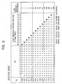
- Fig. 2 of the accompanying drawings shows one example of a light emission driving pattern in one field period, in which each discharge cell is driven based on the light emission driving sequence described above and shown in Fig. 1 of the accompanying drawings (see for example Fig. 27 of Japanese Patent Kokai No. 2000-227778).
- each discharge cell which is initialized to the lit mode in the leading subfield SF1 is set to the extinguished mode during one of the subfields SF1 to SF14, as indicated by a black circle.
- the discharge cell Once the discharge cell is set to the extinguished mode, that discharge cell does not return to the lit mode until the one field period finishes. Hence during the period until the extinguished mode is set, the discharge cell continues the discharging and light emission in the subfields, as indicated by the white circles.
- the total light emission period in one field period is different for each of the 15 light emission patterns shown in Fig. 2, so that 15 intermediate brightnesses are expressed; that is, intermediate brightnesses can be expressed for (N+1) gray scales (where N is the number of subfields).
- each pixel of the input image signal is converted for example into 8-bit pixel data, and the upper 6 bits are taken to be display data while the remaining lower 2 bits are regarded as error data.
- the result of weighted addition of the error data in the pixel data of the surrounding pixels is then reflected in the display data.
- the brightness of the lower 2 bits of the original pixel is pseudo-represented by the surrounding pixels, and consequently only 6 bits of display data, fewer than the original 8 bits, can represent brightness grayscales equivalently to the 8 bits of pixel data.
- the 6 bits of error-diffused pixel data obtained by this error diffusion processing are subjected to dither processing.
- dither processing a plurality of neighboring pixels are regarded as one pixel unit, and dither coefficients consisting of different coefficient values are allocated and added to the error-diffused pixel data corresponding to the pixels within one pixel unit respectively.
- dither coefficients consisting of different coefficient values
- the upper 4 bits of the dither-added pixel data are extracted and used as multi-grayscale pixel data PDs, so as to allocate these pixel data PDs to the 15 light emission patterns, as shown in Fig. 2, respectively.
- dither coefficients are added regularly to pixel data in dither processing, pseudo-patterns not related to the input image signal, i.e., so-called dither patterns, are sometimes perceived. This detracts from the image quality.
- One object of this invention is to provide a driving device for a display panel enabling satisfactory image display with dither patterns suppressed.
- an improved driving device for a display panel.
- pixel cells serving as pixels are positioned in a plurality of display lines.
- the driving device drives the display panel according to pixel data derived from an input image signal.
- the display lines are divided into a plurality of display line groups, and each group includes a plurality of neighboring display lines.
- the driving device has a light emission driving circuit. This circuit causes the pixel cells in each of the neighboring display lines in the respective display line groups to emit light at different brightness levels based on weighting values assigned to the display lines.
- the weighting values are assigned to the display lines such that bias in brightness differences between the pixel cells positioned in neighboring display lines falls within a prescribed range for all neighboring display lines in the display panel.
- a method of grayscale-driving a display panel based on pixel data derived from an input image signal includes a plurality of display lines, with a plurality of pixel cells serving as pixels being arranged on each display line.
- the display lines are divided into L groups by taking every L display lines.
- Each single field display period of the input image signal is divided into a plurality of subfields.
- the grayscale-driving method includes setting the subfields into a lit mode and an unlit mode in K different manners so as to define first to Kth grayscale driving levels.
- Each grayscale driving level includes L brightness levels so that different brightness levels can be allocated to the display lines belonging to the respective display line groups for every grayscale driving level.
- the display panel is operated in accordance with the first to Kth grayscale driving levels.
- the display panel includes a plurality of display lines, with a plurality of pixel cells serving as pixels being arranged on each display line.
- the display lines are divided into a plurality of groups, each display line group consisting of a predetermined number of neighboring display lines.
- Each single field display period of the input image signal is divided into a plurality of subfields.
- the grayscale-driving method includes setting the subfields into a lit mode and an unlit mode in K different manners so as to define first to Kth grayscale driving levels.
- Each grayscale driving level includes the same number of brightness levels as the number of display lines in each display line group so that different brightness levels can be allocated to the display lines in the display line group for every grayscale driving level.
- the display panel is operated in accordance with the first to Kth grayscale driving levels.
- FIG. 3 the configuration of a plasma display device provided with a driving device according to one embodiment of this invention will be described.
- a plasma display panel or PDP 100 includes a front substrate (not shown) serving as the display surface, and a back substrate (not shown) positioned behind the front substrate, with a discharge space between the front and back substrates. The discharge space is charged with discharge gas.
- Strip-shaped row electrodes X 1 to X n and row electrodes Y 1 to Y n parallel to each other and positioned in alternation, are provided on the front substrate.
- Strip-shaped column electrodes D 1 to D m are positioned on the back substrate so as to intersect with the row electrodes X 1 to X n and Y 1 to Y n .
- the PDP 100 has n display lines. Each pair of row electrodes X i and Y i constitutes one display line.
- Discharge cells G serving as pixels are formed at the intersecting portions (including the discharge space) of the row electrode pairs and column electrodes. That is, the PDP 100 has n x m discharge cells, G (1,1) to G (n,m) , arranged in a matrix.
- a pixel data conversion circuit 1 converts an input image signal into for example 6 bits of pixel data PD for each pixel, and supplies the pixel data PD to a multi-grayscale processing circuit 2.
- the multi-grayscale processing circuit 2 includes a line dither offset value generation circuit 21, adder 22, and lower-bit discard circuit 23.
- the line dither offset value generation circuit 21 first divides the first through nth display lines of the PDP 100 into eight groups, in which display lines separated from each other by eight lines, as follows:
- the line dither offset value generation circuit 21 then creates eight line dither offset values LD with values from 0 to 7 for the above mentioned eight groups of display lines respectively.
- the line dither offset value generation circuit 21 repeatedly executes changes in the allocation to each display line group of the line dither offset values LD, for each field and taking eight fields as one cycle, as shown in Fig. 4A through Fig. 4H.
- the line dither offset value generation circuit 21 allocates line dither offset values LD having the values:
- line dither offset values LD are allocated having the values:
- line dither offset values LD are allocated having the values:
- line dither offset values LD are allocated having the values:
- line dither offset values LD are allocated having the values:
- line dither offset values LD are allocated having the values:
- line dither offset values LD are allocated having the values:
- line dither offset values LD are allocated having the values:
- the line dither offset value generation circuit 21 then supplies to the adder 22 the line dither offset values LD allocated to the display lines that have the discharge cells corresponding to the pixel data PD supplied by the pixel data conversion circuit 1.
- the adder 22 adds the line dither offset values LD to the pixel data PD and supplies the resulting value, i.e., a line offset-added pixel data LF, to the lower-bit discard circuit 23.
- the lower-bit discard circuit 23 discards the lowest three bits of the line offset-added pixel data LF, and supplies the remaining upper three bits, as multi-grayscale pixel data MD, to a driving data conversion circuit 3.
- the driving data conversion circuit 3 converts the multi-grayscale pixel data MD into the 4-bit pixel driving data GD according to a data conversion table shown in Fig. 5, and supplies the pixel driving data GD to a memory 4.
- the memory 4 successively receives and stores the 4-bit pixel driving data GD. Each time writing of one image frame (n rows x m columns) of pixel driving data GD 1,1 to GD n,m ends, the memory 4 separates each of the pixel driving data GD 1,1 to GD n,m by bit digit (0th through 3rd bits), and reads out the results, one display line at a time, associated with the subfields SF0 to SF3. Then, the memory 4 supplies one display line's worth (m in number) of pixel driving data bits, as the pixel driving data bits DB1 to DB(m), to a column electrode driving circuit 5.
- the memory 4 reads only the 0th bit of each of the pixel driving data items GD 1,1 to GD n,m one display line at a time, and supplies these bits, as the pixel driving data bits DB1 to DBm, to the column electrode driving circuit 5.
- the memory 4 reads only the 1st bit of each of the pixel driving data items GD 1,1 to GD n,m one display line at a time, and supplies these bits, as the pixel driving data bits DB1 to DBm, to the column electrode driving circuit 5.
- the memory 4 reads only the 2nd bit of each of the pixel driving data items GD 1,1 to GD n,m one display line at a time, and supplies these bits, as the pixel driving data bits DB1 to DBm, to the column electrode driving circuit 5.
- the memory 4 reads only the 3rd bit of each of the pixel driving data items GD 1,1 to GD n,m one display line at a time, and supplies these bits, as the pixel driving data bits DB1 to DBm, to the column electrode driving circuit 5.
- a driving control circuit 6 generates various timing signals for grayscale driving of the PDP 100 according to the light emission driving sequences shown in the following drawings for the respective subfields:
- the driving control circuit 6 then supplies these timing signals to the column electrode driving circuit 5, row electrode Y driving circuit 7, and row electrode x driving circuit 8. It should be noted that the series of driving shown in Fig. 6A through Fig. 6H is executed repeatedly.
- the column electrode driving circuit 5, row electrode Y driving circuit 7, and row electrode X driving circuit 8 generate driving pulses (not shown) so as to drive the PDP 100 as described below according to the timing signals supplied by the driving control circuit 6, and applies these driving pulses to the column electrodes D 1 to D m , row electrodes X 1 to X n , and row electrodes Y 1 to Y n of the PDP 100.
- each of the fields in the input image signal is divided into five subfields SF0 to SF4.
- a reset process R and an addressing process W0 are executed in sequence.
- the reset process R all the discharge cells G (1,1) to G (n,m) of the PDP 100 are caused to undergo a reset discharge simultaneously, to initialize each of the discharge cells G (1,1) to G (n,m) in the lit mode (a state in which a prescribed amount of wall charge is formed).
- the addressing process W0 the discharge cells G positioned in each of the first through nth display lines of the PDP 100 are caused to undergo selective erase discharge, one display line at a time, according to the pixel driving data GD shown in Fig.
- each of the subfields SF1 to SF3 is further divided into eight subfields, namely, SF1 1 to SF1 8 , SF2 1 to SF2 8 , and SF3 1 to SF3 8 .
- the following addressing processes W1 to W8 are executed.
- the discharge cells positioned in the (8N-7)th display lines namely, the first, 9th, 17th, ..., (n-7)th display lines among all the discharge cells G (1,1) to G (n,m) formed in the PDP 100, are selectively caused to undergo erase discharge according to the pixel driving data.
- the discharge cells in which the erase discharge has occurred are set to the extinguished mode, and the discharge cells in which the erase discharge has not occurred maintain the immediately preceding state.
- the discharge cells positioned in the (8N-7)th display lines are set to either the extinguished mode or to the lit mode, according to the pixel driving data.
- the discharge cells positioned in the (8N-6)th display lines namely, the second, 10th, 18th, ..., (n-6)th display lines, are selectively caused to undergo the erase discharge according to the pixel driving data.
- the discharge cells in which the erase discharge has occurred are set to the extinguished mode, and the discharge cells in which the erase discharge has not occurred maintain the immediately preceding state.
- the discharge cells positioned in the (8N-6)th display lines are set to either the extinguished mode or to the lit mode, according to the pixel driving data.
- the discharge cells positioned in the (8N-5)th display lines namely, the third, 11th, 19th, ..., (n-5)th display lines, are selectively caused to undergo the erase discharge according to the pixel driving data.
- the discharge cells in which the erase discharge has occurred are set to the extinguished mode, and the discharge cells in which the erase discharge has not occurred maintain the immediately preceding state. That is, through the addressing process W3, the discharge cells positioned in the (8N-5)th display lines are set to either the extinguished mode or to the lit mode, according to the pixel driving data.
- the discharge cells positioned in the (8N-4)th display lines namely, the 4th, 12th, 20th, ..., (n-4)th display lines, are selectively caused to undergo the erase discharge according to the pixel driving data.
- the discharge cells in which the erase discharge has occurred are set to the extinguished mode, and the discharge cells in which the erase discharge has not occurred maintain the immediately preceding state. That is, through the addressing process W4, the discharge cells positioned in the (8N-4)th display lines are set to either the extinguished mode or to the lit mode, according to the pixel driving data.
- the discharge cells positioned in the (8N-3)th display lines namely, the 5th, 13th, 21th, ..., (n-3)th display lines, are selectively caused to undergo the erase discharge according to the pixel driving data.
- the discharge cells in which the erase discharge has occurred are set to the extinguished mode, and the discharge cells in which the erase discharge has not occurred maintain the immediately preceding state.
- the discharge cells positioned in the (8N-3)th display lines are set to either the extinguished mode or to the lit mode, according to the pixel driving data.
- the discharge cells positioned in the (8N-2)th display lines namely, the 6th, 14th, 22th, ..., (n-2)th display lines, are selectively caused to undergo erase discharge according to the pixel driving data.
- the discharge cells in which the erase discharge has occurred are set to the extinguished mode, and the discharge cells in which the erase discharge has not occurred maintain the immediately preceding state.
- the discharge cells positioned in the (8N-2)th display lines are set to either the extinguished mode or to the lit mode, according to the pixel driving data.
- the discharge cells positioned in the (8N-1)th display lines namely, the 7th, 15th, 23th, ..., (n-1)th display lines, are selectively caused to undergo the erase discharge according to the pixel driving data.
- the discharge cells in which the erase discharge has occurred are set to the extinguished mode, and the discharge cells in which the erase discharge has not occurred maintain the immediately preceding state. That is, through the addressing process W7, the discharge cells positioned in the (8N-1)th display lines are set to either the extinguished mode or to the lit mode, according to the pixel driving data.
- the discharge cells positioned in the (8N)th display lines namely, the 8th, 16th, 24th, ..., nth display lines, are selectively caused to undergo the erase discharge according to the pixel driving data.
- the discharge cells in which the erase discharge has occurred are set to the extinguished mode, and the discharge cells in which the erase discharge has not occurred maintain the immediately preceding state. That is, through the addressing process W8, the discharge cells positioned in the (8N)th display lines are set to either the extinguished mode or to the lit mode, according to the pixel driving data.
- a sustain process I is executed to cause discharge light emission continuously over the period "1" in only the discharge cells set to the lit mode.
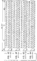
- the driving control circuit 6 performs the light emission driving shown in Fig. 7 through Fig. 14, according to the light emission driving sequences shown in Fig. 6A through Fig. 6H.
- Fig. 7 shows the light emission driving pattern based on the light emission driving sequence of Fig. 6A
- Fig. 8 shows the light emission driving pattern based on the light emission driving sequence of Fig. 6B
- Fig. 9 shows the light emission driving pattern based on the light emission driving sequence of Fig. 6C
- Fig. 10 shows the light emission driving pattern based on the light emission driving sequence of Fig. 6D
- Fig. 11 shows the light emission driving pattern based on the light emission driving sequence of Fig. 6E
- Fig. 12 shows the light emission driving pattern based on the light emission driving sequence of Fig. 6F
- Fig. 13 shows the light emission driving pattern based on the light emission driving sequence of Fig. 6G
- Fig. 14 shows the light emission driving pattern based on the light emission driving sequence of Fig. 6H.
- the 0th bit of the pixel driving data GD is logical level 1, so that in the addressing process W0 of the subfield SF0 the erase discharge (indicated by a black circle) is caused in the discharge cell, and this discharge cell makes a transition to the extinguished mode.
- a transition of a discharge cell during one field display period from the extinguished mode to the lit mode is possible only during the reset process R of the leading subfield SF0.
- a discharge cell which has once made a transition to the extinguished mode is maintained in the extinguished mode throughout the field display period.
- each discharge cell is maintained in the extinguished state throughout the field display period, and driving at the brightness level 0 is performed, as shown in Fig. 15.
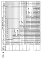
- driving of the discharge cells in the display lines is performed at brightness levels corresponding to the period of light emission generated by the sustain discharge occurring in one field display period; that is, as shown in Fig. 15, driving is performed in the following manner:
- driving of the discharge cells in the display lines is performed at brightness levels corresponding to the period of light emission generated by the sustain discharge occurring in one field display period; that is, as shown in Fig. 15, driving is performed:
- each discharge cell emits light at the brightness level corresponding to the period of light emission generated by the sustain discharge occurring in one field display period; that is, as shown in Fig. 15, the discharge cells are driven to emit light at the following brightness level:
- first through fifth grayscale driving is performed enabling expression of brightnesses in five levels, according to the five pixel driving data GD values "1000", “0100”, “0010”, “0001”, and "0000".
- different brightness weightings are assigned to the eight neighboring display lines, and for each of the first through fifth grayscale driving levels, the neighboring eight display lines are driven at different brightnesses in accordance with the brightness weightings.
- brightness weightings are allocated to the eight neighboring display lines as follows:
- brightness weightings are allocated to the eight neighboring display lines as follows:
- brightness weightings are allocated to the eight neighboring display lines as follows:
- brightness weightings are allocated to the eight neighboring display lines as follows:
- brightness weightings are allocated to the eight neighboring display lines as follows:
- brightness weightings are allocated to the eight neighboring display lines as follows:
- brightness weightings are allocated to the eight neighboring display lines as follows:
- brightness weightings are allocated to the eight neighboring display lines as follows:
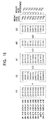
- the line dither offset value generation circuit 21 adds the line dither offset values LD shown in Fig. 4A to the pixel data PD of each display line, as shown in Fig. 16.
- line dither offset values LD line offset-added pixel data LF is obtained for each display line, as shown in Fig. 16; that is,
- the lower-bit discard circuit 23 discards the lower 3 bits of each line offset-added pixel data LF, and takes the remaining upper 3 bits as the multi-grayscale pixel data MD.
- the multi-grayscale pixel data MD is obtained for the eight neighboring display lines as shown in Fig. 16; that is,
- the multi-grayscale pixel data MD is converted by the driving data conversion circuit 3 into 5-bit pixel driving data GD, as follows.
- the discharge cells belonging to the eight neighboring display lines are driven to emit light at the following brightness levels:
- the bias in brightness differences between neighboring display lines in the PDP 100 is rendered approximately uniform.
- the bias is restricted to remain within a prescribed value. For example, if "010100" pixel data PD is supplied, as shown in Fig. 16,
- the bias in brightness differences between neighboring display lines is "2" or less.
- the discharge cells belonging to the eight neighboring display lines emit light at the brightness levels of five grayscales, as shown in Fig. 15.
- the discharge cells positioned in the (8N-7)th display lines are driven to emit light at brightness level "13" by the third grayscale driving, or to emit light at brightness level "21” by the fourth grayscale driving. Consequently when the discharge cells positioned in the (8N-6)th display lines are driven by the third grayscale driving, the brightness difference between the (8N-6)th and (8N-7)th display lines is "3", and when the discharge cells positioned in the (8N-6)th display lines are driven by the fourth grayscale driving, the brightness difference between the (8N-6)th and (8N-7)th display lines is "5".
- the bias in these two values is "2".
- the bias in brightness differences between neighboring display lines is limited to within a prescribed range, so as to obtain a high-quality dithered display with little unevenness in brightness.
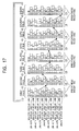
- the first through eighth fields of the input image signal are taken to be one cycle, and in each field the weighting of line dither processing is changed for each of eight neighboring display lines, as shown in Fig. 17.
- the first line dither processing adds a "0" line dither offset value LD to the pixel data PD in addition to performing light emission corresponding to a brightness weighting of "8".
- the second line dither processing adds a "1" line dither offset value LD to the pixel data PD in addition to performing light emission corresponding to a brightness weighting of "7".
- the third line dither processing adds a "2" line dither offset value LD to the pixel data PD in addition to performing light emission corresponding to a brightness weighting of "6";
- the fourth line dither processing adds a "3" line dither offset value LD to the pixel data PD in addition to performing light emission corresponding to a brightness weighting of "5";
- the fifth line dither processing adds a "4" line dither offset value LD to the pixel data PD in addition to performing light emission corresponding to a brightness weighting of "4";
- the sixth line dither processing adds a "5" line dither offset value LD to the pixel data PD in addition to performing light emission corresponding to a brightness weighting of "3";
- the seventh line dither processing adds a "6" line dither offset value LD to the pixel data PD in addition to performing light emission corresponding to a brightness weighting of "2";
- the eighth line dither processing adds a "7" line dither offset value LD to the pixel data PD in addition to performing light emission corresponding to a brightness weighting of "1".
- the first through eighth line dither processing is allocated to the display lines as follows:
- the first through eighth line dither processing is allocated to the display lines as follows:
- the first through eighth line dither processing is allocated to the display lines as follows:
- the first through eighth line dither processing is allocated to the display lines as follows:
- the first through eighth line dither processing is allocated to the display lines as follows:
- the first through eighth line dither processing is allocated to the display lines as follows:
- the first through eighth line dither processing is allocated to the display lines as follows:
- the first through eighth line dither processing is allocated to the display lines as follows:
- each line dither processing is applied to upper and lower display lines alternately in the screen, as the field proceeds.
- the fifth line dither processing in which a line dither offset value LD of "4" is added to the pixel data PD and light emission driving is performed with a brightness weighting of "4" is allocated to the (8N-3)th display line in the first field.
- the fifth line dither processing is performed on the (8N-7)th display line, positioned lower than the (8N-3)th display line in the screen, as indicated by the arrow.
- the fifth line dither processing is performed on the (8N-1)th display line, positioned higher than the (8N-7)th display line, as indicated by the arrow.
- the fifth line dither processing is performed on the (8N-5)th display line, positioned lower than the (8N-1)th display line.
- the fifth line dither processing is performed on the (8N-6)th display line, positioned higher than the (8N-5)th display line, as indicated by the arrow.
- the fifth line dither processing is performed on the (8N-2)th display line, positioned lower than the (8N-6)th display line, as indicated by the arrow.
- the fifth line dither processing is performed on the (8N-4)th display line, positioned higher than the (8N-2)th display line, as indicated by the arrow.
- the fifth line dither processing is performed on the (8N)th display line, positioned lower than the (8N-4)th display line, as indicated by the arrow.
- the display lines are divided into eight display line groups at every eight lines, and correspondingly, subfields SF(k) are divided into eight lower-level subfields SF(k) 1 to SF(k) 8 , to execute eight-line dither processing; however, the number of divisions is not limited to eight, but may be four or six divisions, or similar.
- the display lines are divided into four display line groups at every four lines, as shown below:
Landscapes
- Engineering & Computer Science (AREA)
- Physics & Mathematics (AREA)
- Computer Hardware Design (AREA)
- General Physics & Mathematics (AREA)
- Theoretical Computer Science (AREA)
- Power Engineering (AREA)
- Plasma & Fusion (AREA)
- Control Of Indicators Other Than Cathode Ray Tubes (AREA)
- Controls And Circuits For Display Device (AREA)
- Control Of Gas Discharge Display Tubes (AREA)
- Transforming Electric Information Into Light Information (AREA)
Applications Claiming Priority (2)
| Application Number | Priority Date | Filing Date | Title |
|---|---|---|---|
| JP2003178113 | 2003-06-23 | ||
| JP2003178113A JP4381043B2 (ja) | 2003-06-23 | 2003-06-23 | 表示パネルの駆動装置 |
Publications (2)
| Publication Number | Publication Date |
|---|---|
| EP1492075A2 true EP1492075A2 (de) | 2004-12-29 |
| EP1492075A3 EP1492075A3 (de) | 2008-03-26 |
Family
ID=33411036
Family Applications (1)
| Application Number | Title | Priority Date | Filing Date |
|---|---|---|---|
| EP04013961A Withdrawn EP1492075A3 (de) | 2003-06-23 | 2004-06-15 | Ansteuerschaltung für eine Anzeigetafel |
Country Status (6)
| Country | Link |
|---|---|
| US (1) | US7453477B2 (de) |
| EP (1) | EP1492075A3 (de) |
| JP (1) | JP4381043B2 (de) |
| KR (1) | KR100541204B1 (de) |
| CN (1) | CN1573908A (de) |
| TW (1) | TWI277044B (de) |
Cited By (1)
| Publication number | Priority date | Publication date | Assignee | Title |
|---|---|---|---|---|
| EP1615198A3 (de) * | 2004-07-08 | 2008-03-19 | Pioneer Corporation | Verfahren zur Steuerung einer Anzeigetafel |
Families Citing this family (4)
| Publication number | Priority date | Publication date | Assignee | Title |
|---|---|---|---|---|
| JP4410997B2 (ja) * | 2003-02-20 | 2010-02-10 | パナソニック株式会社 | 表示パネルの駆動装置 |
| JP4731841B2 (ja) * | 2004-06-16 | 2011-07-27 | パナソニック株式会社 | 表示パネルの駆動装置及び駆動方法 |
| US20100186377A1 (en) * | 2007-07-11 | 2010-07-29 | Toyota Jidosha Kabushiki Kaisha | Internal combustion engine exhaust gas control apparatus and control method thereof |
| TWI545552B (zh) | 2014-03-27 | 2016-08-11 | Sitronix Technology Corp | Drive color display display black and white gray image of the drive circuit and its data conversion circuit |
Family Cites Families (11)
| Publication number | Priority date | Publication date | Assignee | Title |
|---|---|---|---|---|
| JP3789052B2 (ja) | 1998-12-03 | 2006-06-21 | パイオニア株式会社 | プラズマディスプレイパネルの駆動方法 |
| JP3730826B2 (ja) * | 1999-10-12 | 2006-01-05 | パイオニア株式会社 | プラズマディスプレイパネルの駆動方法 |
| JP3741417B2 (ja) * | 2000-04-18 | 2006-02-01 | パイオニア株式会社 | ディスプレイパネルの駆動方法 |
| JP3738890B2 (ja) * | 2000-04-27 | 2006-01-25 | パイオニア株式会社 | プラズマディスプレイパネルの駆動方法 |
| JP3736672B2 (ja) * | 2000-05-25 | 2006-01-18 | パイオニア株式会社 | プラズマディスプレイパネルの駆動方法 |
| JP3765381B2 (ja) * | 2000-05-25 | 2006-04-12 | パイオニア株式会社 | プラズマディスプレイ装置 |
| JP4253422B2 (ja) * | 2000-06-05 | 2009-04-15 | パイオニア株式会社 | プラズマディスプレイパネルの駆動方法 |
| JP4410997B2 (ja) * | 2003-02-20 | 2010-02-10 | パナソニック株式会社 | 表示パネルの駆動装置 |
| JP4490656B2 (ja) * | 2003-07-02 | 2010-06-30 | パナソニック株式会社 | 表示パネルの駆動方法 |
| JP2005024912A (ja) * | 2003-07-02 | 2005-01-27 | Pioneer Electronic Corp | 表示パネルの駆動装置 |
| JP4408350B2 (ja) * | 2003-07-07 | 2010-02-03 | パナソニック株式会社 | 表示パネルの駆動方法 |
-
2003
- 2003-06-23 JP JP2003178113A patent/JP4381043B2/ja not_active Expired - Fee Related
-
2004
- 2004-06-15 EP EP04013961A patent/EP1492075A3/de not_active Withdrawn
- 2004-06-15 TW TW093117168A patent/TWI277044B/zh not_active IP Right Cessation
- 2004-06-16 US US10/868,185 patent/US7453477B2/en not_active Expired - Fee Related
- 2004-06-22 KR KR1020040046631A patent/KR100541204B1/ko not_active Expired - Fee Related
- 2004-06-23 CN CNA2004100694752A patent/CN1573908A/zh active Pending
Cited By (2)
| Publication number | Priority date | Publication date | Assignee | Title |
|---|---|---|---|---|
| EP1615198A3 (de) * | 2004-07-08 | 2008-03-19 | Pioneer Corporation | Verfahren zur Steuerung einer Anzeigetafel |
| US7501997B2 (en) | 2004-07-08 | 2009-03-10 | Pioneer Corporation | Method of driving a display panel |
Also Published As
| Publication number | Publication date |
|---|---|
| TW200501007A (en) | 2005-01-01 |
| US20050024350A1 (en) | 2005-02-03 |
| US7453477B2 (en) | 2008-11-18 |
| KR100541204B1 (ko) | 2006-01-12 |
| JP2005017357A (ja) | 2005-01-20 |
| JP4381043B2 (ja) | 2009-12-09 |
| CN1573908A (zh) | 2005-02-02 |
| EP1492075A3 (de) | 2008-03-26 |
| KR20050000339A (ko) | 2005-01-03 |
| TWI277044B (en) | 2007-03-21 |
Similar Documents
| Publication | Publication Date | Title |
|---|---|---|
| JP3750889B2 (ja) | ディスプレイパネルの中間調表示方法 | |
| JP4410997B2 (ja) | 表示パネルの駆動装置 | |
| US7379035B2 (en) | Display panel driver device | |
| US6982732B2 (en) | Display panel driving method with selectable driving pattern | |
| US7453477B2 (en) | Driving device for a display panel | |
| JP3734244B2 (ja) | ディスプレイパネルの駆動方法 | |
| JP4408350B2 (ja) | 表示パネルの駆動方法 | |
| JP4490656B2 (ja) | 表示パネルの駆動方法 | |
| JP3585090B2 (ja) | ディスプレイパネルの中間調表示方法 | |
| KR100740063B1 (ko) | 디스플레이 패널의 구동 방법 | |
| EP1763007A2 (de) | Ansteuerverfahren für eine Anzeigetafel | |
| JP2007102204A (ja) | 表示パネルの駆動方法 | |
| JP2008304599A (ja) | 表示パネルの駆動方法 | |
| JP2008003463A (ja) | 表示パネルの駆動方法 |
Legal Events
| Date | Code | Title | Description |
|---|---|---|---|
| PUAI | Public reference made under article 153(3) epc to a published international application that has entered the european phase |
Free format text: ORIGINAL CODE: 0009012 |
|
| AK | Designated contracting states |
Kind code of ref document: A2 Designated state(s): AT BE BG CH CY CZ DE DK EE ES FI FR GB GR HU IE IT LI LU MC NL PL PT RO SE SI SK TR |
|
| AX | Request for extension of the european patent |
Extension state: AL HR LT LV MK |
|
| PUAL | Search report despatched |
Free format text: ORIGINAL CODE: 0009013 |
|
| AK | Designated contracting states |
Kind code of ref document: A3 Designated state(s): AT BE BG CH CY CZ DE DK EE ES FI FR GB GR HU IE IT LI LU MC NL PL PT RO SE SI SK TR |
|
| AX | Request for extension of the european patent |
Extension state: AL HR LT LV MK |
|
| AKX | Designation fees paid |
Designated state(s): DE FR GB |
|
| STAA | Information on the status of an ep patent application or granted ep patent |
Free format text: STATUS: THE APPLICATION IS DEEMED TO BE WITHDRAWN |
|
| 18D | Application deemed to be withdrawn |
Effective date: 20050630 |