BACKGROUND OF THE INVENTION
1. Field of the Invention
-
The present invention relates to a display device
including a multi-grayscale processing circuit for
subjecting an input video signal to a multi-grayscale
process.
2. Description of the Related Art
-
In recent years, as a two-dimensional image display
panel, a plasma display panel (hereinafter, referred to as
PDP) having a plurality of discharge cells arranged in
matrix has been receiving attention. For displaying any
image corresponding to an input video signal on such a PDP,
a subfield method is known as a driving method. With the
subfield method, the display period of a field is divided
into a plurality of subfields, and on the resulting subfield
basis, the discharge cells are each selectively discharged
for light emission depending on the luminance level of the
input video signal. This allows perception of intermediate
luminance corresponding to the total duration of light
emission in a field period.
-
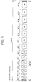
FIG. 1 is a diagram showing an exemplary light
emission driving sequence based on such a subfield method
(refer to FIG. 14 of Japanese Patent Kokai No.2000-227778
(Patent Document 1) as an example).
-
In the light emission driving sequence of FIG. 1, a
field period is divided into fourteen subfields of SF1 to
SF14. Only in the subfield SF1 locating first of those SF1
to SF14, all of the discharge cells of a PDP are initiated
to be in a lighting mode (Rc). On the basis of each subfield
SF1 to SF14, an input video signal is referred to set the
corresponding discharge cells to an extinction mode (Wc),
and only the discharge cells in the lighting mode are
discharged for light emission for the duration allocated to
the subfield (Ic).
-
FIG. 2 is a diagram showing an exemplary light
emission driving pattern in a subfield period of each
discharge cells to be driven based on such an light emission
driving sequence (refer to FIG. 27 of Patent Document 1, for
example).
-
In the light emission pattern of FIG. 2, the discharge
cells initiated to be in the lighting mode in the first
subfield SF1 are set to the extinction mode as shown by
black dots in any one of the subfields SF1 to Sf14. Once set
as such, those are not put back to the lighting mode again.
Thus, the discharge cells continuously discharge for light
emission in the subfields as shown by white dots until set
to the extinction mode. At this time, the fifteen light
emission patterns of FIG. 2 vary in total light emission
duration in a field period, representing fifteen
intermediate luminance levels. That is, achieved thereby is
intermediate luminance display of (N+1) tones (where N is
the number of subfields).
-
The problem with such a driving method is that the
subfields as a result of field division are limited in
number, causing shortage of the number of tones. Thus, to
make up for the tone shortage, the input video signal is
subjected to a multi-grayscale process such as error
diffusion and dithering.
-
First, in the error diffusion process, an input video
signal is converted into pixel data on a pixel basis, for
example pixel data of eight bits. Out of the resulting data,
six significant bits are regarded as display data, and the
remaining two less-significant bits as error data. Then, the
error data of the pixel data derived for each pixel in a
close range is assigned weights and added together, and the
result derived thereby is reflected to the display data.
Through such an operation, as to one original pixel, the
luminance of the less-significant two bits is represented in
a pseudo manner by other pixels therearound, enabling
representation of luminance tone equivalent to pixel data of
eight bits using display data of only six bits. Then, the
error-diffused pixel data of six bits derived by such an
error diffusion process is subjected to dithering. At
dithering, a plurality of adjacent pixels are regarded as a
pixel unit, and to the error-diffused pixel data
corresponding to each pixel in the pixel unit, a dither
coefficient is assigned. The dither coefficients vary in
value, and after such assignment, the dither coefficients
are added together. Through such addition of dither
coefficients, in view of a pixel unit, luminance
representation so far required eight bits can be achieved
only by four significant bits of the dither-added pixel data.
Accordingly, four significant bits of the dither-added
pixel data are extracted, and the extraction result is
assigned to 15 light emission patterns of FIG. 2 as multi-grayscale
pixel data PDs.
-
Here, another problem of image quality degradation
arises if addition of dither coefficient to pixel data is
done regularly by dithering, for example. This is because
pseudo patterns irrelevant to an input video signal, so-called
dither patterns, may be perceived thereby.
-
The present invention is proposed for solving the
above problems, and an object thereof is to provide a
display panel drive capable of satisfactory image display
with dither patterns suppressed.
SUMMARY OF THE INVENTION
-
A first aspect of the present invention is directed to
a display panel drive for tone-driving, responding to pixel
data based on a video signal, a display panel in which a
field display period of the video signal is constituted by a
plurality of subfields, and pixel cells each carrying a
pixel for n (where n is a natural number) display lines are
arranged, the display panel drive comprising: a multi-grayscale
means for deriving multi-grayscale pixel data by
adding each different offset value to the pixel data
corresponding to a display line group including [M · (k-1)+1]th
display lines (where M is a natural number, and k is
a natural number of n/M or smaller) of the display panel, a
display line group including [M · (k-1)+2]th display lines
thereof, a display line group including [M · (k-1)+3]th
display lines thereof, ..., a display line group including
[M · (k-1)+M]th display lines thereof; and an address means
for performing a lighting mode setting or an extinction mode
setting based on the multi-grayscale pixel data with respect
to each of the pixel cells belonging to the corresponding
display line group each different in at least M of the
subfields.
-
A second aspect of the present invention is directed
to a display panel drive for tone-driving, responding to
pixel data based on a video signal, a display panel in which
pixel cells each carrying a pixel for a plurality of display
lines are arranged, the display panel drive comprising: a
multi-grayscale means for deriving multi-grayscale pixel
data by adding each different offset value to the pixel data
each corresponding to m display lines belonging to a display
line group including m (where m is a natural number of 2 or
larger) display lines adjacent to one another; and an light
emission driving means for emitting the pixel cells
depending on the multi-grayscale pixel data by weighing the
display line groups each differently in luminance.
BRIEF DESCRIPTION OF THE DRAWINGS
-
- FIG. 1 is a diagram showing an exemplary light
emission driving sequence based on a subfield method;
- FIG. 2 is a diagram showing an exemplary light
emission driving pattern in a field period of each discharge
cell to be driven based on the light emission driving
sequence of FIG. 1;
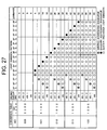
- FIG. 3 is a diagram showing the structure of a plasma
display device as a display device of the present invention;
- FIG. 4 is a diagram showing a data conversion table to
be used in a driving data conversion circuit 3 of FIG. 3,
and an light emission driving pattern in a field period;
- FIG. 5 is a diagram showing an exemplary light
emission driving sequence when a PDP 100 is driven with a
selective deletion address method adopted;
- FIG. 6 is a diagram showing various driving pulses to
be applied to the PDP 100 and their application timings in
subfields SF0 and SF11 to SF14 in accordance with the light
emission driving sequence of FIG. 5;
- FIG. 7 is a diagram showing the operation for driving
the plasma display device of FIG. 3 with the selective
deletion address method adopted when pixel data PD each
corresponding to four adjacent discharge cells all
representing the luminance level of "9";
- FIG. 8 is a diagram schematically showing the
luminance levels covering four tones to be represented,
respectively, by four discharge cells vertically adjacent to
one another in a screen;
- FIG. 9 is a diagram schematically showing the light
emission luminance patterns of four discharge cells
vertically adjacent to one another in a screen, and the
luminance levels to be represented on an light emission
luminance pattern basis;
- FIG. 10 is a diagram schematically showing the light
emission luminance patterns of four discharge cells
vertically adjacent to one another in a screen, and the
luminance levels to be represented on an light emission
luminance pattern basis;
- FIG. 11 is a diagram showing exemplary line offset
data LD and light emission driving sequences at the time of
driving the PDP 100 through change of line offset data LD
and light emission driving sequences on a field basis;
- FIG. 12 is a diagram schematically showing, on a field
basis, the luminance levels covering four tones to be
represented, respectively, by four discharge cells
vertically adjacent to one another in a screen at the time
of driving shown in FIG. 11;
- FIG. 13 is a diagram showing the structure of a plasma
display device as a display device of another embodiment of
the present invention;
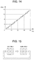
- FIG. 14 is a diagram showing data conversion
characteristics of a first data conversion circuit 11 of FIG.
13;
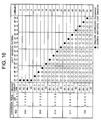
- FIG. 15 is a diagram showing an exemplary dither
coefficient to be occurred in a dither matrix circuit 220 of
FIG. 13;
- FIG. 16 is a diagram showing a data conversion table
to be used in a driving data conversion circuit 30 of FIG.
13, and an light emission driving pattern in a field period;
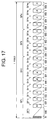
- FIG. 17 is a diagram showing an exemplary light
emission driving sequence at the time of driving the PDP 100
with the selective deletion address method adopted;
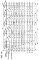
- FIG. 18 is a diagram showing various driving pulses to
be applied to the PDP 100 and their application timings in
subfields SF0 and SF11 to SF14 in accordance with the light
emission driving sequence of FIG. 17;
- FIG. 19 is a diagram showing the operation for driving
the plasma display device of FIG. 13 with the selective
deletion address method adopted when pixel data PD each
corresponding to eight adjacent discharge cells all
representing the luminance level of "32";
- FIG. 20 is a diagram schematically showing the
luminance levels covering four tones to be represented,
respectively, by four discharge cells vertically adjacent to
one another in a screen in the plasma display device of FIG.
13;
- FIG. 21 is a diagram schematically showing the light
emission luminance patterns of four discharge cells in the
plasma display device of FIG. 13, and the luminance levels
to be represented on an light emission luminance pattern
basis;
- FIG. 22 is a diagram schematically showing the light
emission luminance patterns of four discharge cells in the
plasma display device of FIG. 13, and the luminance levels
to be represented on an light emission luminance pattern
basis;
- FIG. 23 is a diagram showing an exemplary light
emission driving sequence at the time of driving the PDP 100
with a selective writing address method adopted;
- FIG. 24 is a diagram showing a data conversion table
to be used in the driving data conversion circuit 30 of FIG.
13, and an light emission driving pattern in a field period
when the selective writing address method is adopted;
- FIG. 25 is a diagram showing the operation for driving
the plasma display device of FIG. 13 with the selective
writing address method adopted when pixel data PD each
corresponding to eight adjacent discharge cells all
representing the luminance level of "32";
- FIG. 26 is a diagram showing an exemplary light
emission driving sequence at the time of driving the PDP 100
with the selective writing address method and the selective
deletion address method combined;
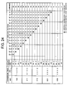
- FIG. 27 is a diagram showing a data conversion table
to be used in the driving data conversion circuit 30 at the
time of driving the PDP 100 in accordance with the light
emission driving sequence of FIG. 26, and an light emission
driving pattern in a field period;
- FIG. 28 is a diagram showing the structure of a plasma
display device as a display device of another embodiment of
the present invention;
- FIG. 29 is a diagram showing data conversion
characteristics of a first data conversion circuit 13 of FIG.
28;
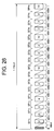
- FIG. 30 is a diagram showing exemplary offset data LD
each corresponding to eight discharge lines vertically
adjacent to one another in a screen;
- FIG. 31 is a diagram showing an exemplary light
emission driving sequence at the time of driving the PDP 100
of FIG. 28 based on the selective deletion address method;
and
- FIG. 32 is a diagram showing an exemplary light
emission driving sequence at the time of driving the PDP 100
of FIG. 28 based on the selective writing address method.
-
DETAILED DESCRIPTION OF THE INVENTION
-
In the below, embodiments of the present invention are
described by referring to the accompanying drawings.
-
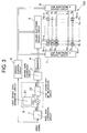
FIG. 3 is a diagram showing the schematic structure of
a plasma display device as a display device of the present
invention.
-
In FIG. 3, a PDP 100 being a plasma display panel
includes a front substrate (not shown) serving as a display
plane and a rear substrate (not shown) opposing to the front
substrate with a discharge-gas-filled discharge space
therebetween. The front substrate is formed with strip-shaped
row electrodes X1 to Xn and Y1 to Yn arranged
alternately and parallel with one another. Formed on the
rear substrate are strip-shaped column electrodes D1 to Dm
intersected on the row electrodes X1 to Xn and Y1 to Yn.
Herein, as to the row electrodes X1 to Xn and Y1 to Yn, each
pair of row electrodes X and Y serves as a display line of
the PDP 100, from the 1st line to the nth line. At an
intersection part (discharge space included) of a pair of
row electrode and column electrode, formed is a discharge
cell G serving as a pixel. That is, the PDP 100 includes (n
× m) discharge cells G(1, 1) to G(n, m) formed in a matrix.
-
A pixel data conversion circuit 1 converts an input
video signal into pixel data PD on a pixel basis, for
example pixel data of six bits. Then, the resulting data is
supplied to a multi-grayscale processing circuit 2, which is
constituted by a line offset data generation circuit 21, an
adder 22, and a less-significant bit truncation circuit 23.
-
When the pixel data conversion circuit 1 outputs pixel
data PD corresponding to the (4N-3)th display lines [N:
natural number of (1/4) · n or smaller] of the PDP 100, the
line offset data generation circuit 21 generates line offset
data LD representing "10" (decimal numeral). Thus generated
data is supplied to the adder 22. Similarly, when the pixel
data conversion circuit 1 outputs pixel data PD
corresponding to the (4N-2)th display lines, the line offset
data generation circuit 21 generates line offset data LD
representing "8" (decimal numeral) for supply to the adder
22. When the pixel data conversion circuit 1 outputs pixel
data PD corresponding to the (4N-1)th display lines, the
line offset data generation circuit 21 generates line offset
data LD representing "6" (decimal numeral) for supply to the
adder 22. Further, when the pixel data conversion circuit 1
outputs pixel data PD corresponding to the (4N)th display
lines, the line offset data generation circuit 21 generates
line offset data LD representing "4" (decimal numeral) for
supply to the adder 22.
-
To the pixel data PD provided by the pixel data
conversion circuit 1, the adder 22 adds the corresponding
line offset data LD. The resulting offset-added pixel data
is then supplied to the less-significant bit truncation
circuit 23. The less-significant bit truncation circuit 23
truncates three less-significant bits of the offset-added
pixel data, and the remaining three significant bits are
supplied to a driving data conversion circuit 3 as multi-grayscale
pixel data MD.
-
The driving data conversion circuit 3 converts thus
provided multi-grayscale pixel data MD into pixel driving
data GD of five bits in accordance with a data conversion
table shown in FIG. 4. The resulting data is then supplied
to memory 4.
-
The memory 4 sequentially receives and stores the
pixel driving data GD of five bits. Every time completing
writing of pixel driving data GD1,1 to GDn,m of an image frame
(n lines × m columns), the memory 4 separates each of the
pixel driving data GD1,1 to GDn,m on a bit digit (1st to 5th
bits) basis. Then, the memory 4 performs reading on a
display line basis corresponding to subfields SF1 to SF4,
which will be described later. The memory 4 then supplies,
to a column electrode driving circuit 5, pixel driving data
bits of thus read one display line (m bits) as pixel driving
data bits DB1 to DB(m).
-
To be more specific, first in a subfield SF11, the
memory 4 reads only the 1st bit of the pixel driving data
GD1,1 to GDn,m for every display line. Thus read results are
supplied to the column electrode driving circuit 5 as the
pixel driving data bits DB1 to DB(m). Then, in subfields
SF12 to SF21, the memory 4 reads only the 2nd bit of the
pixel driving data GD1,1 to GDn,m for every display line, and
thus read results are supplied to the column electrode
driving circuit 5 as the pixel driving data bits DB1 to
DB(m). Next, in subfields SF22 to SF31, the memory 4 reads
only the 3rd bit of the pixel driving data GD1,1 to GDn,m for
every display line for supply to the column electrode .
driving circuit 5 as the pixel driving data bits DB1 to
DB(m). Then, in subfields SF32 to SF41, the memory 4 reads
only the 4th bit of the pixel driving data GD1,1 to GDn,m for
every display line for supply to the column electrode
driving circuit 5 as the pixel driving data bits DB1 to
DB(m). And, in subfields SF42 to SF44, the memory 4 reads
only the 5th bit of the pixel driving data GD1,1 to GDn,m for
every display line for supply to the column electrode
driving circuit 5 as the pixel driving data bits DB1 to
DB(m).
-
In accordance with an light emission driving sequence
of FIG. 5 based on the subfield method, a driving control
circuit 6 supplies various timing signals for tone-driving
the PDP 100 to the column electrode driving circuit 5, a row
electrode Y driving circuit 7, and a row electrode X driving
circuit 8.
-
In the light emission driving sequence of FIG. 5, the
display period of a field is divided into the subfields SF1
to SF4, and for each of the subfields, various driving
processes are carried out as below. Note here that, the
subfields SF1 to SF4 are constituted by, respectively, four
subfields of SF11 to SF14, SF21 to SF24, SF31 to SF34, SF41 to
SF44 as shown in FIG. 5.
-
First, in the first subfield SF11, a reset process R,
an address process W0, and a sustain process I are carried
out. Specifically, in the reset process R, every discharge
cell of the PDP 100 is initiated to be in a lighting mode
(state of predetermined wall charge being formed). In the
address process W0, the discharge cells are selectively
shifted to be in an extinction mode (state of wall charge
being eliminated) with respect to every display line
depending on the pixel driving data. And in the sustain
process I, only the discharge cells in the lighting mode are
discharged for light emission continuously over the period
of "2".
-
In each of the subfields SF21, SF31, and SF41, an
address process W4 and the sustain process I are carried out.
Specifically, in the address process W4, the discharge
cells belonging to the (4N)th display lines are selectively
shifted to the extinction mode depending on the pixel
driving data. In the sustain process I, only the discharge
cells in the lighting mode are discharged for light emission
continuously over the period of "2".
-
In each of the subfields SF12, SF22, SF32, and SF42,
carried out are an address process W1 and the sustain
process I. Specifically, in the address process W1, the
discharge cells belonging to the (4N-3)th display lines are
selectively shifted to the extinction mode depending on the
pixel driving data. In the sustain process I, only the
discharge cells in the lighting mode are discharged for
light emission continuously over the period of "2".
-
In each of the subfields SF13, SF23, SF33, and SF43,
carried out are an address process W2 and the sustain
process I. Specifically, in the address process W2, the
discharge cells belonging to the (4N-2)th display lines are
selectively shifted to the extinction mode depending on the
pixel driving data. In the sustain process I, only the
discharge cells in the lighting mode are discharged for
light emission continuously over the period of "2".
-
In each of the subfields SF14, SF24, SF34, and SF44,
carried out are an address process W3 and the sustain
process I. Specifically, in the address process W3, the
discharge cells belonging to the (4N-1)th display lines are
selectively shifted to the extinction mode depending on the
pixel driving data. In the sustain process I, only the
discharge cells in the lighting mode are discharged for
light emission continuously over the period of "2".
-
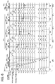
FIG. 6 is a diagram showing various driving pulses to
be applied to the PDP 100, and their application timings in
accordance with such an light emission driving sequence.
Such application is made by the column electrode driving
circuit 5, the row electrode Y driving circuit 7, and the
row electrode X driving circuit 8 responding to various
timing signals provided by the driving control circuit 6.
Here, in the subfields SF21, SF31, and SF41, the various
driving pulses to be applied to the PDP 100 and their
application timings are all the same. In the subfields SF12,
SF22, SF32, and SF42, the various driving pulses to be
applied to the PDP 100 and their application timings are all
the same. In the subfields SF13, SF23, SF33, and SF43, the
various driving pulses to be applied to the PDP 100 and
their application timings are all the same. Further, in the
subfields SF14, SF24, SF34, and SF44, the various driving
pulses to be applied to the PDP 100 and their application
timings are all the same. Therefore, FIG. 6 shows only the
subfield SF11 to the address process W4 in the subfield SF21.
-
First in the reset process R in the subfield SF11, the
row electrode X driving circuit 8 generates a negative reset
pulse RPx showing mild falling edge change. Thus generated
pulse is applied to the row electrodes X1 to Xn of the PDP
100. At the same time as such a reset pulse RPx, the row
electrode Y driving circuit 7 generates a positive reset
pulse RPy showing mild rising edge change for application to
the row electrodes Y1 to Yn of the PDP 100. Such
simultaneous application of the reset pulses RPx and RPy
responsively causes reset discharge to occur to every
discharge cell of the PDP 100, resultantly forming wall
charge in each of the discharge cells. In this manner, all
of the discharge cells are initiated to be in the lighting
mode, being emissive state (light light emission responding
to sustain discharge) in the sustain process I (described
below).
-
Next, in the address process W0 in the subfield SF11,
the row electrode Y driving circuit 7 sequentially applies a
negative scanning pulse SP to the row electrodes Y1 to Yn.
During this time, the column electrode driving circuit 5
generates m pixel data pulses for a display line
corresponding to the pixel driving data bits DB1 to DB(m)
read from the memory 4. Then, a pixel data pulse group DP
consisted of thus generated m pixel data pulses is applied
to the column electrodes D1 to Dm, respectively, in
synchronization with the scanning pulse SP. That is, as
shown in FIG. 6, sequentially applied to the column
electrodes D1 to Dm are pixel data pulse groups DP1 to DPn
corresponding to the 1st to nth display lines of the PDP 100,
respectively. Here, the pixel data pulse generated by the
column electrode driving circuit 5 is high in voltage when
the pixel driving data bit DB is in the logic level 1, and
when in the logic level 0, the pixel data pulse will be low
in voltage. At this time, erasure addressing discharge
occurs only to the discharge cells locating at intersections
of the display lines and the column electrodes. Here, the
display lines are those having applied with the scanning
pulse SP, and the column electrodes are those having applied
with the pixel data pulse of high voltage. Through such
erasure addressing discharge, the wall charge so far formed
in the discharge cells is eliminated, and the resulting
discharge cells shift into the extinction mode, being non-emissive
state (light emission responding to sustain
discharge) in the sustain process I (described below). On
the other hand, no such erasure addressing discharge occurs
to the discharge cells having applied with the scanning
pulse SP and with the pixel data pulse but of low voltage,
and thus the mode immediately before (lighting or extinction
mode) is sustained.
-
That is, in the address process W0, all of the
discharge cells of the PDP 100 are selectively put to cause
erasure addressing discharge based on the pixel data. In
this manner, the discharge cells are each set to be in
either the lighting mode or the extinction mode.
-
Next, in the sustain process I in the subfield SF11,
the row electrode X driving circuit 8 and the row electrode
Y driving circuit 7 alternately apply positive sustain
pulses IPx and IPy repeatedly for a predetermined number of
times to the row electrodes X1 to Xn and Y1 to Yn as shown in
FIG. 6. At this time, in response to every application of
the sustain pulses IPx and IPy, sustain discharge occurs only
to the discharge cells with the wall charge remained therein,
i.e., the discharge cells set in the lighting mode. Those
discharge cells sustain the light emission state resulting
from such sustain discharge. To be more specific, only the
discharge cells sustaining the state of the lighting mode
without erasure addressing discharge occurring in the
address process W0 in the subfield SF11 emit in the sustain
process I over the predetermined period of "2".
-
Then, in the address process W1 in the subfield SF12,
the row electrode Y driving circuit 7 sequentially applies a
negative scanning pulse SP to any row electrode Y belonging
to the (4N-3)th display lines [N: 1 to (1/4) · n] of the PDP
100, i.e., the row electrodes Y1, Y5, Y9, ..., Y(n-3) · During
this time, the column electrode driving circuit 5 generates
m pixel data pulses for a display line corresponding to the
pixel driving data bits DB1 to DB(m) read from the memory 4.
Then, the pixel data pulse group DP consisted of the
resulting m pixel data pulses is applied to the column
electrodes D1 to Dm in synchronization with the scanning
pulse SP. At this time, in the subfield SF12, read from the
memory 4 is the pixel driving data bit DB corresponding to
the (4N-3)th display lines of the PDP 100. Accordingly, the
column electrode driving circuit 5 sequentially applies the
pixel data pulse groups DP1, DP5, DP9, ..., DP(n-3)
corresponding to the (4N-3)th display lines to the column
electrodes D1 to Dm as shown in FIG. 6. Here, the pixel data
pulse generated by the column electrode driving circuit 5 is
high in voltage when the pixel driving data bit DB is in the
logic level 1, and when in the logic level 0, the pixel data
pulse will be low in voltage. At this time, erasure
addressing discharge occurs only to the discharge cells
locating at intersections of the display lines and the
column electrodes. Here, the display lines are those having
applied with the scanning pulse SP, and the column
electrodes are those having applied with the pixel data
pulse of high voltage. Through such erasure addressing
discharge, the wall charge so far formed in the discharge
cells is eliminated, and the resulting discharge cells shift
into the extinction mode, being non-emissive state (light
emission responding to sustain discharge) in the sustain
process I. On the other hand, no such erasure addressing
discharge occurs to the discharge cells having applied with
the scanning pulse SP and with the pixel data pulse but of
low voltage, and thus the mode immediately before (lighting
or extinction mode) is sustained.
-
That is, in the address process W1, only the discharge
cells belonging to the (4N-3)th display lines of the PDP 100
are selectively put to cause erasure addressing discharge
based on the pixel data. In this manner, the discharge cells
are each set to be in either the lighting mode or the
extinction mode.
-
Next, in the sustain process I in the subfield SF12,
the row electrode X driving circuit 8 and the row electrode'
Y driving circuit 7 alternately apply positive sustain
pulses IPx and IPy repeatedly for a predetermined number of
times to the row electrodes X1 to Xn and Y1 to Yn as shown in
FIG. 6. At this time, in response to every application of
the sustain pulses IPx and IPy, sustain discharge occurs only
to the discharge cells with the wall charge remained therein,
i.e., the discharge cells set in the lighting mode. Those
discharge cells sustain the light emission state resulting
from such sustain discharge. To be more specific, only the
discharge cells sustaining the state of the lighting mode
without erasure addressing discharge occurring in both the
address processes W0 and W1 emit in the sustain process I
over the predetermined period of "2".
-
Then, in the address process W2 in the subfield SF13,
the row electrode Y driving circuit 7 sequentially applies a
negative scanning pulse SP to any row electrode Y belonging
to the (4N-2)th display lines [N: natural number of (1/4) · n
or smaller] of the PDP 100, i.e., the row electrodes Y2, Y6,
Y10, ..., Y(n-2). During this time, the column electrode
driving circuit 5 generates m pixel data pulses for a display
line corresponding to the pixel driving data bits DB1 to
DB(m) read from the memory 4. Then, the pixel data pulse
group DP consisted of the resulting m pixel data pulses is
applied to the column electrodes D1 to Dm in synchronization
with the scanning pulse SP. At this time, in the subfield .
SF13, read from the memory 4 is the pixel driving data bit DB
corresponding to the (4N-2)th display lines of the PDP 100.
Accordingly, the column electrode driving circuit 5
sequentially applies the pixel data pulse groups DP2, DP6,
DP10, ..., DP(n-2) corresponding to the (4N-2) th display lines
to the column electrodes D1 to Dm as shown in FIG. 6. Here,
the pixel data pulse generated by the column electrode
driving circuit 5 is high in voltage when the pixel driving
data bit DB is in the logic level 1, and when in the logic
level 0, the pixel data pulse will be low in voltage. At
this time, erasure addressing discharge occurs only to the
discharge cells locating at intersections of the display
lines and the column electrodes. Here, the display lines are
those having applied with the scanning pulse SP, and the
column electrodes are those having applied with the pixel
data pulse of high voltage. Through such erasure addressing
discharge, the wall charge so far formed in the discharge
cells is eliminated, and the resulting discharge cells shift
into the extinction mode. On the other hand, no such erasure
addressing discharge occurs to the discharge cells having
applied with the scanning pulse SP and with the pixel data
pulse but of low voltage, and thus the mode immediately
before (lighting or extinction mode) is sustained.
-
That is, in the address process W2, only the discharge
cells belonging to the (4N-2)th display lines of the PDP 100
are selectively put to cause erasure addressing discharge
based on the pixel data. In this manner, the discharge cells
are each set to be in either the lighting mode or the
extinction mode.
-
Next, in the sustain process I in the subfield SF13,
the row electrode X driving circuit 8 and the row electrode Y
driving circuit 7 alternately apply positive sustain pulses
IPx and IPy repeatedly for a predetermined number of times to
the row electrodes X1 to Xn and Y1 to Yn as shown in FIG. 6.
At this time, in response to every application of the sustain
pulses IPx and IPy, sustain discharge occurs only to the
discharge cells with the wall charge remained therein, i.e.,
the discharge cells set in the lighting mode. Those
discharge cells sustain the light emission state resulting
from such sustain discharge. To be more specific, only the
discharge cells sustaining the state of the lighting mode
without erasure addressing discharge occurring in the address
processes W0, W1, and W2 emit in the sustain process I over
the predetermined period of "2".
-
Then, in the address process W3 in the subfield SF14,
the row electrode Y driving circuit 7 sequentially applies a
negative scanning pulse SP to any row electrode Y belonging
to the (4N-1)th display lines [N: natural number of (1/4) · n
or smaller] of the PDP 100, i.e., the row electrodes Y3, Y7,
Y11, ... , Y(n-1) · During this time, the column electrode
driving circuit 5 generates m pixel data pulses for a display
line corresponding to the pixel driving data bits DB1 to
DB(m) read from the memory 4. Then, the pixel data pulse
group DP consisted of the resulting m pixel data pulses is
applied to the column electrodes D1 to Dm in synchronization
with the scanning pulse SP. At this time, in the subfield
SF14, read from the memory 4 is the pixel driving data bit DB
corresponding to the (4N-1)th display lines of the PDP 100.
Accordingly, the column electrode driving circuit 5
sequentially applies the pixel data pulse groups DP3, DP7,
DP11, ..., DP(n-1) corresponding to the (4N-1)th display lines
to the column electrodes D1 to Dm as shown in FIG. 6. Here,
the pixel data pulse generated by the column electrode
driving circuit 5 is high in voltage when the pixel driving
data bit DB is in the logic level 1, and when in the logic
level 0, the pixel data pulse will be low in voltage. At
this time, erasure addressing discharge occurs only to the
discharge cells locating at intersections of the display
lines and the column electrodes. Here, the display lines are
those having applied with the scanning pulse SP, and the
column electrodes are those having applied with the pixel
data pulse of high voltage. Through such erasure addressing
discharge, the wall charge so far formed in the discharge
cells is eliminated, and the resulting discharge cells shift
into the extinction mode. On the other hand, no such erasure
addressing discharge occurs to the discharge cells having ,
applied with the scanning pulse SP and with the pixel data
pulse but of low voltage, and thus the mode immediately
before (lighting or extinction mode) is sustained.
-
That is, in the address process W3, only the discharge
cells belonging to the (4N-1)th display lines of the PDP 100
are selectively put to cause erasure addressing discharge
based on the pixel data. In this manner, the discharge cells
are each set to be in either the lighting mode or the
extinction mode.
-
Next, in the sustain process I in the subfield SF14,
the row electrode X driving circuit 8 and the row electrode Y
driving circuit 7 alternately apply positive sustain pulses
IPx and IPy repeatedly for a predetermined number of times to
the row electrodes X1 to Xn and Y1 to Yn as shown in FIG. 6.
At this time, in response to every application of the sustain
pulses IPx and IPy, sustain discharge occurs only to the
discharge cells with the wall charge remained therein, i.e.,
the discharge cells set in the lighting mode. Those
discharge cells sustain the light emission state resulting
from such sustain discharge. To be more specific, only the
discharge cells sustaining the state of the lighting mode
without erasure addressing discharge occurring in the address
processes W0, W1, W2, and W3 emit in the sustain process I
over the predetermined period of "2".
-
Then, in the address process W4 in the subfield SF21,
the row electrode Y driving circuit 7 sequentially applies a
negative scanning pulse SP to any row electrode Y belonging
to the (4N)th display lines [N: 1 to (1/4) · n] of the PDP
100, i.e., the row electrodes Y4, Y8, Y12, ..., Yn. During
this time, the column electrode driving circuit 5 generates m
pixel data pulses for a display line corresponding to the
pixel driving data bits DB1 to DB(m) read from the memory 4.
Then, the pixel data pulse group DP consisted of the
resulting m pixel data pulses is applied to the column
electrodes D1 to Dm in synchronization with the scanning
pulse SP. At this time, in the subfield SF21, read from the
memory 4 is the pixel driving data bit DB corresponding to
the (4N)th display lines of the PDP 100. Accordingly, the
column electrode driving circuit 5 sequentially applies the
pixel data pulse groups DP4, DP8, DP12, ..., DPn corresponding
to the (4N)th display lines to the column electrodes D1 to Dm
as shown in FIG. 6. Here, the pixel data pulse generated by
the column electrode driving circuit 5 is high in voltage
when the pixel driving data bit DB is in the logic level 1,
and when in the logic level 0, the pixel data pulse will be
low in voltage. At this time, erasure addressing discharge
occurs only to the discharge cells locating at intersections
of the display lines and the column electrodes. Here, the
display lines are those having applied with the scanning
pulse SP, and the column electrodes are those having applied
with the pixel data pulse of high voltage. Through such
erasure addressing discharge, the wall charge so far formed
in the discharge cells is eliminated, and the resulting
discharge cells shift into the extinction mode. On the other
hand, no such erasure addressing discharge occurs to the
discharge cells having applied with the scanning pulse SP and
with the pixel data pulse but of low voltage, and thus the
mode immediately before (lighting or extinction mode) is
sustained.
-
That is, in the address process W4, only the discharge
cells belonging to the (4N)th display lines of the PDP 100
are selectively put to cause erasure addressing discharge
based on the pixel data. In this manner, the discharge cells
are each set to be in either the lighting mode or the
extinction mode.
-
Next, in the sustain process I (not shown) in the
subfield SF21, the row electrode X driving circuit 8 and the
row electrode Y driving circuit 7 alternately apply positive
sustain pulses IPx and IPy repeatedly for a predetermined
number of times to the row electrodes X1 to Xn and Y1 to Yn.
At this time, in response to every application of the sustain
pulses IPx and IPy, sustain discharge occurs only to the
discharge cells with the wall charge remained therein, i.e.,
the discharge cells set in the lighting mode. Those
discharge cells sustain the light emission state resulting
from such sustain discharge. To be more specific, only the
discharge cells sustaining the state of the lighting mode
without erasure addressing discharge occurring in the address
processes W0, W1, W2, W3, and W4 emit in the sustain process
I over the predetermined period of "2".
-
By going through such driving, among the subfield
groups SF1 to SF4, only the reset process R in the first
subfield SF11 allows the discharge cells to shift from the
extinction mode to the lighting mode. In other words, once
the discharge cells are set to be in the extinction mode
responding to the erasure addressing discharge occurring in
each first subfield, the discharge cells are not allowed to
be in the lighting mode again in the following subfields.
Thus, by going through driving based on the 5 pixel driving
data GD as shown in FIG. 4, the discharge cells are set to be
in the lighting mode in the sequential subfields by the
corresponding luminance to be represented. Then, until
erasure addressing discharge occurs (indicated by black dots),
sustain discharge light emission (indicated by white dots)
occurs continually in the sustain process I in the respective
subfields. During this time, perceived is the intermediate
luminance corresponding to the total light emission duration
in one field period caused by such sustain discharge light
emission.
-
Here, with driving shown in FIGS. 5 and 6, the
discharge cells belonging to four display lines vertically
adjacent to one another in the screen of the PDP 100, i.e.,
for each of these
discharge cells belonging to (4N-3)th display lines,
discharge cells belonging to (4N-2)th display lines,
discharge cells belonging to (4N-1)th display lines,
and
discharge cells belonging to (4N)th display lines,
the total light emission duration differs in each field
period responding to the driving based on the pixel driving
data GD.
-
Taking pixel driving data GD [00100] of FIG. 4 as an
example, the discharge cells belonging to the (4N-3)th
display lines, i.e., 1st, 5th, 9th, ..., and (n-3)th display
lines, are put to cause sustain discharge for light emission
in the sustain process I of the subfields SF11 to SF14, and
SF21 as indicated by white dots. The discharge cells
belonging to the (4N-2)th display lines, i.e., 2nd, 6th,
10th, ..., and (n-2)th display lines, are put to cause
sustain discharge for light emission in the sustain process I
of the subfields SF11 to SF14, SF21, and SF22. The discharge
cells belonging to the (4N-1)th display lines, i.e., 3rd, 7th,
11th, ..., and (n-1)th display lines, are put to cause
sustain discharge for light emission in the sustain process I
of the subfields SF11 to SF14, and SF21 to SF23. Further, the
discharge cells belonging to the (4N)th display lines, i.e.,
4th, 8th, 12th, ..., and nth display lines, are put to cause
sustain discharge for light emission in the sustain process I
of the subfields SF11 to SF14, and SF21 to SF24.
-
During this time, assuming that the light emission
duration in each sustain process I is "2", the total light
emission duration in one field period caused by sustain
discharge light emission occurred responding to the pixel
driving data GD of [00100] will be as follows, as shown in
FIG. 4,
discharge cells belonging to (4N-3)th display lines: "10",
discharge cells belonging to (4N-2)th display lines: "12",
discharge cells belonging to (4N-1)th display lines: "14",
and
discharge cells belonging to (4N)th display lines: "16".
-
Similarly, the total light emission duration in one
field period caused by sustain discharge light emission
occurred responding to the pixel driving data GD of [01000]
as shown in FIG. 4 will be as follows:
- discharge cells belonging to (4N-3)th display lines: "2",
- discharge cells belonging to (4N-2)th display lines: "4",
- discharge cells belonging to (4N-1)th display lines: "6",
and
- discharge cells belonging to (4N)th display lines: "8".
-
-
That is, four adjacent display lines are driven in each
different manner to vary the total light emission duration on
a field period basis.
-
Note here that, with such driving, for the purpose of
equalizing the average luminance level for four discharge
cells vertically adjacent to one another in the screen, the
pixel data PD is added with the line offset data LD.
-
Specifically, first of all, added is such line offset
data LD as
"10" to pixel data PD corresponding to (4N-3)th display
lines,
"8" to pixel data PD corresponding to (4N-2)th display
lines,
"6" to pixel data PD corresponding to (4N-1)th display
lines, and
"4" to pixel data PD corresponding to (4N)th display lines.
-
Then, out of the addition result, three significant
bits are regarded as multi-grayscale pixel data MD, which is
converted into pixel driving data GD in accordance with the
conversion table of FIG. 4.
-
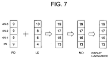
For example, assuming here that pixel data PD(1,1), PD(2,1),
PD(3,1), and PD(4,1) corresponding, respectively, to discharge
cells G(1,1), G(2,1), G(3,1), and G(4,1) vertically adjacent to one
another in the screen of the PDP 100 are all six-bit data
[001001] representing "9" (decimal numeral). Through addition
of the line offset data LD of "10", "8", "4", and "2" as shown
in FIG. 7 respectively to PD(1,1), PD(2,1), PD(3,1), and PD(4,1),
derived are the addition results as
six-bit data of [010011] representing "19",
six-bit data of [010001] representing "17",
six-bit data of [001111] representing "15", and
six-bit data of [001101] representing "13".
-
Here, from each of the addition results, extracting
three significant bits by truncating the three less-significant
bits will lead to
three-bit multi-grayscale pixel data MD(1, 1) of [010]
representing "2",
three-bit multi-grayscale pixel data MD(2, 1) of [010]
representing "2",
three--bit multi-grayscale pixel data MD(3, 1) of [001] ,
representing "1", and
three-bit multi-grayscale pixel data MD(4, 1) of [001]
representing "1".
-
Accordingly, with the multi-grayscale pixel data MD(1,1)
of [010] as such, the discharge cell G(1,1) belonging to the
(4N-3)th display lines is put to cause sustain discharge for
light emission in the sustain processes I in the subfields
SF11 to SF14, and SF21 as indicated by the white dots of FIG.
4. As a result, perceived is the light emission luminance of
"10". With the multi-grayscale pixel data MD(2,1) of [010], the
discharge cell G(2,1) belonging to the (4N-2)th display lines
is put to cause sustain discharge for light emission in the
sustain processes I in the subfields SF11 to SF14, SF21, and
SF22. As a result, perceived is the light emission luminance
of "12". With the multi-grayscale pixel data MD(3,1) of [001],
the discharge cell G(3,1) belonging to the (4N-1)th display
lines is put to cause sustain discharge for light emission in
the sustain processes I in the subfields SF11 to SF13 as
indicated by the white dots of FIG. 4. As a result,
perceived is the light emission luminance of "6". Further,
with the multi-grayscale pixel data MD(4,1) of [001], the
discharge cell G(4,1) belonging to the (4N)th display lines is
put to cause sustain discharge for light emission in the
sustain processes I in the subfields SF11 to SF14 as
indicated by the white dots of FIG. 4. As a result,
perceived is the light emission luminance of "8".
-
As such, responding to the incoming pixel data PD
representing the luminance level of "9", the four discharge
cells G
(1,1)' G
(2,1), G
(3,1) , and G
(4,1) vertically adjacent to one
another in the screen of the
PDP 100 each emit representing
as follows:
- G(1,1) : luminance level "10",
- G(2,1) : luminance level "12",
- G(3,1) : luminance level "6", and
- G(4,1) : luminance level "8".
-
-
In view of these four discharge cells G as a unit,
perceived is the luminance level of "9" being an average
value of the luminance levels. That is, represented is the
luminance of the incoming video signal (pixel data PD).
-
As described in the foregoing, in such a plasma display
device as shown in FIG. 3, for each of the (4N-3)th display
lines, the (4N-2)th display lines, the (4N-1)th display lines,
and the (4N)th display lines of the PDP 100, light emission
driving is so applied as to represent each different four
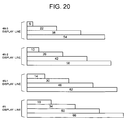
luminance levels as shown in FIG. 8. Here, in view of four
discharge cells G vertically adjacent to one another in a
screen as a unit, perceived are 17 intermediate luminance
levels as shown in FIGS. 9 and 10 in accordance with an
average value of the luminance levels represented for every
discharge cell G in a single unit. At this time, the
luminance levels to be represented by the vertically-adjacent
four discharge cells G in a screen are all varied. Thus,
even if the line offset data LD serving as the dither
coefficient is added to the pixel data corresponding to each
of these four discharge cells G, dither patterns can be
preferably prevented from occurring.
-
In the above embodiment, the line offset data LD being
"10", "8", "6", and "4" are assigned, for addition, to pixel
data PD corresponding to the (4N-3)th display lines, the (4N-2)th
display lines, the (4N-1)th display lines, and the
(4N)th display lines. This is not surely restrictive, and
such assignment may be made on a field basis as shown in FIG.
11.
-
That is, in the 1st field, added is the line offset
data LD as follows:
- "10" to pixel data PD corresponding to (4N-3)th display
lines,
- "8" to pixel data PD corresponding to (4N-2)th display
lines,
- "6" to pixel data PD corresponding to (4N-1)th display
lines, and
- "4" to pixel data PD corresponding to (4N)th display
lines.
-
-
In the 2nd field, added is the line offset data LD as
follows:
- "8" to pixel data PD corresponding to (4N-3)th display,
lines,
- "6" to pixel data PD corresponding to (4N-2)th display
lines,
- "4" to pixel data PD corresponding to (4N-1)th display
lines, and
- "10" to pixel data PD corresponding to (4N)th display
lines.
-
-
In the 3rd field, added is the line offset data LD as
follows:
- "6" to pixel data PD corresponding to (4N-3)th display
lines,
- "4" to pixel data PD corresponding to (4N-2)th display
lines,
- "10" to pixel data PD corresponding to (4N-1)th display
lines, and
- "8" to pixel data PD corresponding to (4N)th display
lines.
-
-
Then in the 4th field, added is the line offset data LD
as follows:
- "4" to pixel data PD corresponding to (4N-3)th display
lines,
- "10" to pixel data PD corresponding to (4N-2)th display
lines,
- "8" to pixel data PD corresponding to (4N-1)th display
lines, and
- "6" to pixel data PD corresponding to (4N)th display
lines.
-
-
Further, in response to such assignment change of the
line offset data LD, as shown in FIG. 11, the light emission
driving sequence to be adopted is changed for the 1st to 4th
fields. Specifically, in the 1st field, executed is driving
in accordance with such an light emission driving sequence as
shown in FIG. 5. In the 2nd to 4th fields, the address
process is changed in execution order in the subfields SF12
to SF14, SF21 to SF24, SF31 to SF34, and SF41 to SF 44 shown in
Fig. 5.
-
For example, in the 2nd field, executed in the subfield
SF11 is the address process W0 to every display line
similarly to the light emission driving sequence shown in FIG.
5. In the subfields SF21, SF31, and SF41, executed is the
address process W3 to the (4N-1)th display lines, in the
subfields SF12, SF22, SF 32, and SF42, executed is the address
process W4 to the (4N)th display lines, in the subfields SF13,
SF23, SF33, and SF43, executed is the address process W1 to
the (4N-3)th display lines, and in the subfields SF14, SF24,
SF34, and SF44, executed is the address process W2 to the
(4N-2)th display lines.
-
In the 3rd field, executed in the subfield SF11 is the
address process W0 to every display line similarly to the
light emission driving sequence shown in FIG. 5. In the
subfields SF21, SF31, and SF41, executed is the address
process W2 to the (4N-2)th display lines, in the subfields
SF12, SF22, SF 32, and SF42, executed is the address process
W3 to the (4N-1)th display lines, in the subfields SF13, SF23,
SF33, and SF43, executed is the address process W4 to the
(4N)th display lines, and in the subfields SF14, SF24, SF34,
and SF44, executed is the address process W1 to the (4N-3)th
display lines.
-
Also, in the 4th field, executed in the subfield SF11
is the address process W0 to every display line similarly to
the light emission driving sequence shown in FIG. 5. In the
subfields SF21, SF31, and SF41, executed is the address
process W1 to the (4N-3)th display lines, in the subfields
SF12, SF22, SF32, and SF42, executed is the address process W2
to the (4N-2)th display lines, in the subfields SF13, SF23,
SF33, and SF43, executed is the address process W3 to the
(4N-1)th display lines, and in the subfields SF14, SF24, SF34,
and SF44, executed is the address process W4 to the (4N)th
display lines.
-
With such driving, the (4N-3)th display lines, the (4N-2)th
display lines, the (4N-1)th display lines, and the
(4N)th display lines vary in luminance levels of 4 stages on
a field basis as shown in FIG. 12. Accordingly, this
considerably reduces the dithering pattern from occurring.
-
FIG. 13 is a diagram showing the schematic structure of
a plasma display device according to another embodiment of
the present invention.
-
In FIG. 13, the PDP 100 being a plasma display panel
includes a front substrate (not shown) serving as a display
plane and a rear substrate (not shown) opposing to the front
substrate with a discharge-gas-filled discharge space
therebetween. The front substrate is formed with strip-shaped
row electrodes X1 to Xn and Y1 to Yn arranged
alternately and parallel with one another. Formed on the
rear substrate are strip-shaped column electrodes D1 to Dm
intersected on the row electrodes X1 to Xn and Y1 to Yn.
Herein, as to the row electrodes X1 to Xn and Y1 to Yn, each
pair of row electrodes X and Y serves as a display line of .
the PDP 100, from 1st to nth. At an intersection part
(discharge space included) of a pair of row electrode and
column electrode, formed is a discharge cell G serving as a
pixel. That is, the PDP 100 includes (n x m) discharge cells
G(1,1) to G(n, m) formed in a matrix.
-
A pixel data conversion circuit 10 converts an input
video signal into pixel data PD on a pixel basis, for example
pixel data of six bits. Then, the resulting data is supplied
to a first data conversion circuit 11, which converts the
pixel data PD into first conversion pixel data PD1 of five
bits in accordance with such conversion characteristics as
shown in FIG. 14. The resulting data is supplied to a multi-grayscale
processing circuit 20. Note here that, in FIG. 14,
the pixel data PD and the first conversion pixel data PD1 are
each represented by decimal numeral.
-
The multi-grayscale processing circuit 20 is
constituted by an adder 200, a line offset data generation
circuit 210, a dither matrix circuit 220, and a less-significant
bit truncation circuit 230.
-
When the first data conversion circuit 11 outputs first
conversion pixel data PD1 corresponding to the (4N-3)th
display lines [N: natural number of (1/4) · n or smaller] of
the PDP 100, the line offset data generation circuit 210
generates line offset data LD representing "3" (decimal
numeral). Thus generated data is supplied to the adder 200.
Similarly, when the first data conversion circuit 11 output's
first conversion pixel data PD1 corresponding to the (4N-2)th
display lines, the line offset data generation circuit 210
generates line offset data LD representing "2" (decimal
numeral) for supply to the adder 200. When the first data
conversion circuit 11 outputs first conversion pixel data PD1
corresponding to the (4N-1)th display lines, the line offset
data generation circuit 210 generates line offset data LD
representing "1" (decimal numeral) for supply to the adder
200. Further, when the first data conversion circuit 11
outputs first conversion pixel data PD1 corresponding to the
(4N)th display lines, the line offset data generation circuit
210 generates line offset data LD representing "0" (decimal
numeral) for supply to the adder 200.
-
On the basis of each pixel group constituted by four
pixels adjacent to one another in the vertical and lateral
directions of the screen, the dither matrix circuit 220
generates a dither coefficient of "0" or "2" (decimal
numeral) as shown in FIG. 15 for each pixel in the pixel
group. The resulting dither coefficients are provided to the
adder 200. Herein, the dither matrix circuit 220 changes
such dither coefficient assignment for each pixel in the
pixel group on a field basis as shown in FIG. 15.
-
The adder 200 adds the dither coefficient to the first
conversion pixel data PD1 of five bits provided by the first
data conversion circuit 11, deriving dither-added pixel data.
To the dither-added pixel data, the adder 200 adds the line
offset data LD for supply to the less-significant bit
truncation circuit 230.
-
The less-significant bit truncation circuit 230
truncates two less-significant bits of the dither-added pixel
data having added with the line offset data LD, and the
remaining three significant bits are provided to a driving
data conversion circuit 30 as multi-grayscale pixel data MD.
-
The driving data conversion circuit 30 converts the
multi-grayscale pixel data MD into pixel driving data GD of
five bits in accordance with a data conversion table shown in
FIG. 16. The resulting data is supplied to memory 40.
-
The memory 40 sequentially receives and stores the
pixel driving data GD of five bits. Every time completing
writing of pixel driving data GD1,1 to GDn,m of an image frame
(n lines × m columns), the memory 40 separates each of the
pixel driving data GD1,1 to GDn,m on a bit digit (1st to 5th
bits) basis. Then, the memory 40 performs reading on a
display line basis corresponding to subfields SF1 to SF4,
which will be described later. The memory 40 then supplies,
to a column electrode driving circuit 50, the pixel driving
data bits of thus read one display line (m bits) as pixel
driving data bits DB1 to DB(m). To be more specific, first
in a subfield SF11, the memory 40 reads only the 1st bit of
the pixel driving data GD1,1 to GDn,m, for every display line.
Thus read results are supplied to the column electrode
driving circuit 50 as pixel driving data bits DB1 to DB(m).
Then, in subfields SF12 to SF21, the memory 40 reads only the
2nd bit of the pixel driving data GD1,1 to GDn,m for every
display line, and thus read results are supplied to the
column electrode driving circuit 50 as the pixel driving data
bits DB1 to DB(m). Next, in subfields SF22 to SF31, the
memory 40 reads only the 3rd bit of the pixel driving data
GD1,1 to GDn,m for every display line, and thus read results
are supplied to the column electrode driving circuit 50 as
the pixel driving data bits DB1 to DB(m). Then, in subfields
SF32 to SF41, the memory 40 reads only the 4th bit of the
pixel driving data GD1,1 to GDn,m for every display line, and
thus read results are supplied to the column electrode
driving circuit 50 as the pixel driving data bits DB1 to
DB (m) . And, in subfields SF42 to SF44, the memory 40 reads
only the 5th bit of the pixel driving data GD1,1 to GDn,m for
every display line, and thus read results are supplied to the
column electrode driving circuit 50 as the pixel driving data
bits DB1 to DB(m).
-
In accordance with such an light emission driving
sequence as shown in FIG. 17 based on the subfield method, a
driving control circuit 60 supplies various timing signals
for tone-driving the PDP 100 to the column electrode driving
circuit 50, a row electrode Y driving circuit 70, and a row
electrode X driving circuit 80.
-
In the light emission driving sequence of FIG. 17, the
display period of a field is divided into the subfields SF1
to SF4, and for each of the subfields, various driving
processes as below are carried out. Note here that, the
subfields SF1 to SF4 are constituted by, respectively, four
subfields of SF11 to SF14, SF21 to SF24, SF31 to SF34, SF41 to
SF44 as shown in FIG. 17.
-
First, in the first subfield SF11, a reset process R,
an address process W0, and a sustain process I are carried
out. Specifically, in the reset process R, every discharge
cell of the PDP 100 is initiated to be in a lighting mode
(state of predetermined wall charge being formed). In the
address process W0, the discharge cells are selectively
shifted to be in an extinction mode (state of wall charge
being eliminated) with respect to every display line
depending on the pixel driving data. And in the sustain
process I, only the discharge cells in the lighting mode are
discharged for light emission continuously over the period of
"6".
-
In each of the subfields SF21, SF31, and SF41, an
address process W4 and the sustain process I are carried out.
Specifically, in the address process W4, the discharge cells
belonging to the (4N)th display lines are selectively shifted
to the extinction mode depending on the pixel driving data.
In the sustain process I, only the discharge cells in the
lighting mode are discharged for light emission continuously
over the period of "4".
-
In each of the subfields SF12, SF22, SF32, and SF42,
carried out are an address process W1 and the sustain process
I. Specifically, in the address process W1, the discharge
cells belonging to the (4N-3)th display lines are selectively
shifted to the extinction mode depending on the pixel driving
data. In the sustain process I, only the discharge cells in
the lighting mode are discharged for light emission
continuously over the period of "4".
-
In each of the subfields SF13, SF23, SF33, and SF43,
carried out are an address process W2 and the sustain process
I. Specifically, in the address process W2, the discharge
cells belonging to the (4N-2)th display lines are selectively
shifted to the extinction mode depending on the pixel driving
data. In the sustain process I, only the discharge cells in
the lighting mode are discharged for light emission
continuously over the period of "4".
-
In each of the subfields SF14, SF24, SF34, and SF44,
carried out are an address process W3 and the sustain process
I. Specifically, in the address process W3, the discharge
cells belonging to the (4N-1)th display lines are selectively
shifted to the extinction mode depending on the pixel driving
data. In the sustain process I, only the discharge cells in
the lighting mode are discharged for light emission
continuously over the period of "4".
-
FIG. 18 is a diagram showing various driving pulses to
be applied to the PDP 100, and their application timings in
accordance with such an light emission driving sequence.
Such application is made by the column electrode driving
circuit 50, the row electrode Y driving circuit 70, and the
row electrode X driving circuit 80. Here, in the subfields
SF21, SF31, and SF41, the various driving pulses to be applied
to the PDP 100 and their application timings are all the same.
In the subfields SF12, SF22, SF32, and SF42, the various
driving pulses to be applied to the PDP 100 and their
application timings are all the same. In the subfields SF13;
SF23, SF33, and SF43, the various driving pulses to be applied
to the PDP 100 and their application timings are all the same.
Further, in the subfields SF14, SF24, SF34, and SF44, the
various driving pulses to be applied to the PDP 100 and their
application timings are all the same. Therefore, FIG. 18
shows only the subfield SF11 to the address process W4 in the
subfield SF21.
-
First in the reset process R in the subfield SF11, the
row electrode X driving circuit 80 generates a negative reset
pulse RPx showing mild falling edge change. Thus generated
pulse is applied to the row electrodes X1 to Xn of the PDP
100. At the same time as such a reset pulse RPx, the row
electrode Y driving circuit 70 generates a positive reset
pulse RPy showing mild rising edge change for application to
the row electrodes Y1 to Yn of the PDP 100. Such simultaneous
application of the reset pulses RPx and RPy responsively
causes reset discharge to occur to every discharge cell of
the PDP 100, resultantly forming wall charge in each of the
discharge cells. In this manner, all of the discharge cells
are initiated to be in the lighting mode, being emissive
state (light emission responding to sustain discharge) in the
sustain process I (described below).
-
Next, in the address process W0 in the subfield SF11,
the row electrode Y driving circuit 70 sequentially applies a
negative scanning pulse SP to the row electrodes Y1 to Yn.
During this time, the column electrode driving circuit 50
generates m pixel data pulses for a display line
corresponding to pixel driving data bits DB1 to DB(m) read
from the memory 40. Then, a pixel data pulse group DP
consisted of thus generated m pixel data pulses is applied to
the column electrodes D1 to Dm, respectively, in
synchronization with the scanning pulse SP. That is, as
shown in FIG. 18, sequentially applied to the column
electrodes D1 to Dm are pixel data pulse groups DP1 to DPn
corresponding to the 1st to nth display lines of the PDP 100,
respectively. Here, the pixel data pulse generated by the
column electrode driving circuit 50 is high in voltage when
the pixel driving data bit DB is in the logic level 1, and
when in the logic level 0, the pixel data pulse will be low
in voltage. At this time, erasure addressing discharge
occurs only to the discharge cells locating at intersections
of the display lines and the column electrodes. Here, the
display lines are those having applied with the scanning
pulse SP, and the column electrodes are those having applied
with the pixel data pulse of high voltage. Through such
erasure addressing discharge, the wall charge so far formed
in the discharge cells is eliminated, and the resulting
discharge cells shift into the extinction mode, being non-emissive
state (light emission responding to sustain
discharge) in the sustain process I (described below). On
the other hand, no such erasure addressing discharge occurs
to the discharge cells having applied with the scanning pulse
SP with the pixel data pulse but of low voltage, and thus the
mode immediately before (lighting or extinction mode) is
sustained.
-
That is, in the address process W0, all of the
discharge cells of the PDP 100 are selectively put to cause
erasure addressing discharge based on the pixel data. In
this manner, the discharge cells are each set to be in either
the lighting mode or the extinction mode.
-
Next, in the sustain process I in the subfield SF11,
the row electrode X driving circuit 80 and the row electrode
Y driving circuit 70 alternately apply positive sustain
pulses IPx and IPy repeatedly for a predetermined number of
times to the row electrodes X1 to Xn and Y1 to Yn as shown in
FIG. 18. At this time, in response to every application of
the sustain pulses IPx and IPy, sustain discharge occurs only
to the discharge cells with the wall charge remained therein,
i.e., the discharge cells set to be in the lighting mode.
Those discharge cells sustain the light emission state
resulting from such sustain discharge. To be more specific,
only the discharge cells sustaining the state of the lighting
mode without erasure addressing discharge occurring in the
address process W0 in the subfield SF11 emit in the sustain
process I over the predetermined period of "6".
-
Then, in the address process W1 in the subfield SF12,
the row electrode Y driving circuit 70 sequentially applies'a
negative scanning pulse SP to any row electrode Y belonging
to the (4N-3)th display lines [N: 1 to (1/4) , · n] of the PDP
100, i.e., the row electrodes Y1, Y5, Y9, ..., Y(n-3) . During
this time, the column electrode driving circuit 50 generates
m pixel data pulses for a display line corresponding to the
pixel driving data bits DB1 to DB(m) read from the memory 40.
Then, the pixel data pulse group DP consisted of the
resulting m pixel data pulses is applied to the column
electrodes D1 to Dm in synchronization with the scanning
pulse SP. At this time, in the subfield SF12, read from the
memory 40 is the pixel driving data bit DB corresponding to
the (4N-3)th display lines of the PDP 100. Accordingly, the
column electrode driving circuit 50 sequentially applies the
pixel data pulse groups DP1, DP5, DP9, ..., DP(n-3)
corresponding to the (4N-3)th display lines to the column
electrodes D1 to Dm as shown in FIG. 18. Here, the pixel data
pulse generated by the column electrode driving circuit 50 is
high in voltage when the pixel driving data bit DB is in the
logic level 1, and when in the logic level 0, the pixel data
pulse will be low in voltage. At this time, erasure
addressing discharge occurs only to the discharge cells
locating at intersections of the display lines and the column
electrodes. Here, the display lines are those having applied
with the scanning pulse SP, and the column electrodes are
those having applied with the pixel data pulse of high
voltage. Through such erasure addressing discharge, the wall
charge so far formed in the discharge cells is eliminated,
and the resulting discharge cells shift into the extinction
mode, being non-emissive state (light emission responding to
sustain discharge) in the sustain process I (described below).
On the other hand, no such erasure addressing discharge
occurs to the discharge cells having applied with the
scanning pulse SP and with the pixel data pulse but of low
voltage, and thus the mode immediately before (lighting or
extinction mode) is sustained.
-
That is, in the address process W1, only the discharge
cells belonging to the (4N-3)th display lines of the PDP 100
are selectively put to cause erasure addressing discharge
based on the pixel data. In this manner, the discharge cells
are each set to be in either the lighting mode or the
extinction mode.
-
Next, in the sustain process I in the subfield SF12,
the row electrode X driving circuit 80 and the row electrode
Y driving circuit 70 alternately apply positive sustain
pulses IPx and IPy repeatedly for a predetermined number of
times to the row electrodes X1 to Xn and Y1 to Yn as shown in
FIG. 18. At this time, in response to every application of
the sustain pulses IPx and IPy, sustain discharge occurs only
to the discharge cells with the wall charge remained therein,
i.e., the discharge cells set in the lighting mode. Those
discharge cells sustain the light emission state resulting ,
from such sustain discharge. To be more specific, only the
discharge cells sustaining the state of the lighting mode
without erasure addressing discharge occurring in the address
processes W0 and W1 emit in the sustain process I over the
predetermined period of "4".
-
Then, in the address process W2 in the subfield SF13,
the row electrode Y driving circuit 70 sequentially applies a
negative scanning pulse SP to any row electrode Y belonging
to the (4N-2)th display lines [N: 1 to (1/4) n] of the PDP
100, i . e . , the row electrodes Y2, Y6, Y10, ..., Y(n-2) . During
this time, the column electrode driving circuit 50 generates
m pixel data pulses for a display line corresponding to the
pixel driving data bits DB1 to DB(m) read from the memory 40.
Then, the pixel data pulse group DP consisted of the ,
resulting m pixel data pulses is applied to the column
electrodes D1 to Dm in synchronization with the scanning
pulse SP. At this time, in the subfield SF13, read from the
memory 40 is the pixel driving data bit DB corresponding to
the (4N-2)th display lines of the PDP 100. Accordingly, the
column electrode driving circuit 50 sequentially applies the
pixel data pulse groups DP2, DP6, DP10, ..., DP(n-2)
corresponding to the (4N-2)th display lines to the column
electrodes D1 to Dm as shown in FIG. 18. Here, the pixel data
pulse generated by the column electrode driving circuit 50 is
high in voltage when the pixel driving data bit DB is in the
logic level 1, and when in the logic level 0, the pixel data
pulse will be low in voltage. At this time, erasure
addressing discharge occurs only to the discharge cells
locating at intersections of the display lines and the column
electrodes. Here, the display lines are those having applied
with the scanning pulse SP, and the column electrodes are
those having applied with the pixel data pulse of high
voltage. Through such erasure addressing discharge, the wall
charge so far formed in the discharge cells is eliminated,
and the resulting discharge cells shift into the extinction
mode. On the other hand, no such erasure addressing
discharge occurs to the discharge cells having applied with'
the scanning pulse SP and with the pixel data pulse but of
low voltage, and thus the mode immediately before (lighting
or extinction mode) is sustained.
-
That is, in the address process W2, only the discharge
cells belonging to the (4N-2)th display lines of the PDP 100
are selectively put to cause erasure addressing discharge
based on the pixel data. In this manner, the discharge cells
are each set to be in either the lighting mode or the
extinction mode.
-
Next, in the sustain process I in the subfield SF13,
the row electrode X driving circuit 80 and the row electrode
Y driving circuit 70 alternately apply positive sustain
pulses IPx and IPy repeatedly for a predetermined number of
times to the row electrodes X1 to Xn and Y1 to Yn as shown in
FIG. 18. At this time, in response to every application of
the sustain pulses IPx and IPy, sustain discharge occurs only
to the discharge cells with the wall charge remained therein,
i.e., the discharge cells set in the lighting mode. Those
discharge cells sustain the light emission state resulting
from such sustain discharge. To be more specific, only the
discharge cells sustaining the state of the lighting mode
without erasure addressing discharge occurring in the address
processes W0, W1, and W2 emit in the sustain process I over
the predetermined period of "4".
-
Then, in the address process W3 in the subfield SF14,
the row electrode Y driving circuit 70 sequentially applies a
negative scanning pulse SP to any row electrode Y belonging
to the (4N-1)th display lines [N: 1 to (1/4) · n] of the PDP
100, i . e . , the row electrodes Y3, Y7, Y11, ..., Y(n-1) . During
this time, the column electrode driving circuit 50 generates
m pixel data pulses for a display line corresponding to the
pixel driving data bits DB1 to DB(m) read from the memory 40.
Then, the pixel data pulse group DP consisted of the
resulting m pixel data pulses is applied to the column
electrodes D1 to Dm in synchronization with the scanning
pulse SP. At this time, in the subfield SF14, read from the
memory 40 is the pixel driving data bit DB corresponding to
the (4N-1)th display lines of the PDP 100. Accordingly, the
column electrode driving circuit 50 sequentially applies the
pixel data pulse groups DP3, DP7, DP11, ..., DP(n-1)
corresponding to the (4N-1)th display lines to the column
electrodes D1 to Dm in as shown in FIG. 18. Here, the pixel
data pulse generated by the column electrode driving circuit
50 is high in voltage when the pixel driving data bit DB is
in the logic level 1, and when in the logic level 0, the
pixel data pulse will be low in voltage. At this time,
erasure addressing discharge occurs only to the discharge
cells locating at intersections of the display lines and the
column electrodes. Here, the display lines are those having
applied with the scanning pulse SP, and the column electrodes
are those having applied with the pixel data pulse of high
voltage. Through such erasure addressing discharge, the wall
charge so far formed in the discharge cells is eliminated,
and the resulting discharge cells shift into the extinction
mode. On the other hand, no such erasure addressing
discharge occurs to the discharge cells having applied with
the scanning pulse SP and with the pixel data pulse but of
low voltage, and thus the mode immediately before (lighting
or extinction mode) is sustained.
-
That is, in the address process W3, only the discharge
cells belonging to the (4N-1)th display lines of the PDP 100
are selectively put to cause erasure addressing discharge
based on the pixel data. In this manner, the discharge cells
are each set to be in either the lighting mode or the
extinction mode.
-
Next, in the sustain process I in the subfield SF14,
the row electrode X driving circuit 80 and the row electrode
Y driving circuit 70 alternately apply positive sustain
pulses IPx and IPy repeatedly for a predetermined number of
times to the row electrodes X1 to Xn and Y1 to Yn as shown in
FIG. 18. At this time, in response to every application of
the sustain pulses IPx and IPy, sustain discharge occurs only
to the discharge cells with the wall charge remained therein,
i.e., the discharge cells set in the lighting mode. Those
discharge cells sustain the light emission state resulting
from such sustain discharge. To be more specific, only the
discharge cells sustaining the state of the lighting mode
without erasure addressing discharge occurring in the address
processes W0, W1, W2, and W3 emit in the sustain process I
over the predetermined period of "4".
-
Then, in the address process W4 in the subfield SF21,
the row electrode Y driving circuit 70 sequentially applies a
negative scanning pulse SP to any row electrode Y belonging
to the (4N)th display lines [N: 1 to (1/4) · n] of the PDP
100, i.e., the row electrodes Y4, Y8, Y12, ..., Yn. During
this time, the column electrode driving circuit 50 generates
m pixel data pulses for a display line corresponding to the
pixel driving data bits DB1 to DB(m) read from the memory 40.
Then, the pixel data pulse group DP consisted of the
resulting m pixel data pulses is applied to the column
electrodes D1 to Dm in synchronization with the scanning
pulse SP. At this time, in the subfield SF21, read from the
memory 40 is the pixel driving data bit DB corresponding to
the (4N)th display lines of the PDP 100. Accordingly, the
column electrode driving circuit 50 sequentially applies the
pixel data pulse groups DP4, DP8, DP12, ..., DPn corresponding
to the (4N)th display lines to the column electrodes D1 to Dm
as shown in FIG. 18. Here, the pixel data pulse generated by
the column electrode driving circuit 50 is high in voltage
when the pixel driving data bit DB is in the logic level 1,
and when in the logic level 0, the pixel data pulse will be
low in voltage. At this time, erasure addressing discharge
occurs only to the discharge cells locating at intersections
of the display lines and the column electrodes. Here, the
display lines are those having applied with the scanning
pulse SP, and the column electrodes are those having applied
with the pixel data pulse of high voltage. Through such
erasure addressing discharge, the wall charge so far formed
in the discharge cells is eliminated, and the resulting
discharge cells shift into the extinction mode. On the other
hand, no such erasure addressing discharge occurs to the
discharge cells having applied with the scanning pulse SP and
with the pixel data pulse but of low voltage, and thus the
mode immediately before (lighting or extinction mode) is
sustained.
-
That is, in the address process W4, only the discharge
cells belonging to the (4N)th display lines of the PDP 100
are selectively put to cause erasure addressing discharge
based on the pixel data. In this manner, the discharge cells
are each set to be in either the lighting mode or the
extinction mode.
-
Next, in the sustain process I (not shown) in the
subfield SF21, the row electrode X driving circuit 80 and the
row electrode Y driving circuit 70 alternately apply positive
sustain pulses IPx and IPy repeatedly for a predetermined
number of times to the row electrodes X1 to Xn and Y1 to Yn.
At this time, in response to every application of the sustain
pulses IPx and IPy, sustain discharge occurs only to the
discharge cells with the wall charge remained therein, i.e.,
the discharge cells set in the lighting mode. Those
discharge cells sustain the light emission state resulting
from such sustain discharge. To be more specific, only the
discharge cells sustaining the state of the lighting mode
without erasure addressing discharge occurring in the address
processes W0, W1, W2, W3, and W4 emit in the sustain process
I over the predetermined period of "4".
-
By going through such driving, among the subfields SF1
to SF4, only the reset process R in the first subfield SF1
allows the discharge cells to shift from the extinction mode
to the lighting mode. In other words, once the discharge
cells are set to be in the extinction mode responding to the
erasure addressing discharge occurring in each first subfield,
the discharge cells are not allowed to be in the lighting
mode again in the following subfields. Thus, by going
through driving based on 5 pixel driving data GD as shown in
FIG. 16, the discharge cells are set to be in the lighting
mode in the sequential subfields by the corresponding
luminance to be represented. Then, until erasure addressing
discharge occurs (indicated by black dots), sustain discharge
light emission (indicated by white dots) occurs continually
in the sustain process I in the respective subfields. During
this time, perceived is the intermediate luminance
corresponding to the total light emission duration in one
field period caused by such sustain discharge light emission.
-
Here, with driving shown in FIGS. 17 and 18, the
discharge cells belonging to four display lines vertically
adjacent to one another in the screen of the PDP 100, i.e.,
for each of these
discharge cells belonging to (4N-3)th display lines,
discharge cells belonging to (4N-2)th display lines,
discharge cells belonging to (4N-1)th display lines,
and
discharge cells belonging to (4N)th display lines,
the total light emission duration differs in each field
period responding to the driving according to the pixel
driving data GD.
-
Taking pixel driving data GD of [00100] of FIG. 16 as.
an example, the discharge cells belonging to the (4N-3)th
display lines, i.e., 1st, 5th, 9th, ..., and (n-3)th display
lines, are put to cause sustain discharge for light emission
in the sustain processes I of the subfields SF11 to SF14, and
SF21 as indicated by white dots. The discharge cells
belonging to the (4N-2)th display lines, i.e., 2nd, 6th,
10th, ..., and (n-2)th display lines, are put to cause
sustain discharge for light emission in the sustain processes
I of the subfields SF11 to SF14, SF21, and SF22. The discharge
cells belonging to the (4N-1)th display lines, i.e., 3rd, 7th,
11th, ..., and (n-1)th display lines, are put to cause
sustain discharge for light emission in the sustain processes
I of the subfields SF11 to SF14, and SF21 to SF23. Further,
the discharge cells belonging to the (4N)th display lines,
i.e., 4th, 8th, 12th, ..., and nth display lines, are put to
cause sustain discharge for light emission in the sustain
processes I of the subfields SF11 to SF14, and SF21 to SF24.
-
Therefore, assuming that the light emission duration in
the sustain processes I of the subfield SF11 is "6", and the
light emission duration in the sustain processes I of other
subfields is "4", the total light emission duration in one
field period caused by sustain discharge light emission
occurred responding to the pixel driving data GD of [00100]
will be as follows, as shown in FIG. 16,
discharge cells belonging to (4N-3)th display lines:
"22",
discharge cells belonging to (4N-2)th display lines:
"26",
discharge cells belonging to (4N-1)th display lines:
"30", and
discharge cells belonging to (4N)th display lines: "34".
-
Similarly, the total light emission duration in one
field period caused by sustain discharge light emission
occurred responding to the pixel driving data GD of [01000]
will be as follows, as shown in FIG. 16,
discharge cells belonging to (4N-3)th display lines:
"6",
discharge cells belonging to (4N-2)th display lines:
"10",
discharge cells belonging to (4N-1)th display lines:
"14", and
discharge cells belonging to (4N)th display lines: "18".
-
That is, four adjacent display lines are driven in each
different manner to vary the total light emission duration on
a field period basis.
-
Note here that, with such driving, for the purpose of
equalizing the average luminance level for four discharge
cells vertically adjacent to one another in the screen,
dither-added pixel data derived by adding a dither
coefficient to the pixel data PD is added with the line
offset data LD.
-
For example, assuming here that pixel data PD
corresponding, respectively, to discharge cells G(1,1), G(2,1),
G(3,1), and G(4,1) vertically adjacent to one another in the
screen of the PDP 100, and discharge cells G(1,2), G(2,2), G(3,2),
G(4,2) locating thereright all are six-bit data representing
"32" (decimal numeral) as shown in FIG. 19. First, the pixel
data PD representing "32" is converted into first conversion
pixel data PD1 of five bits representing "8" by the first
data conversion circuit 11 with such conversion
characteristics as shown in FIG. 14. Next, through addition
of a dither coefficient of "0" or "2", and the line offset
data LD of "3", "2", "1", and "0" as shown in FIG. 19
respectively to the first conversion pixel data PD1
corresponding to the discharge cells G(1,1)' G(2,1), G(3,1), G(4,1),
G(1,2), G(2,2), G(3,2), and G(4,2), derived are the addition results
as
dither-added pixel data of [010011] representing "11",
dither-added pixel data of [01100] representing "12",
dither-added pixel data of [01001] representing "9",
dither-added pixel data of [01010] representing "10",
dither-added pixel data of [01101] representing "13",
dither-added pixel data of [01010] representing "10",
dither-added pixel data of [01011] representing "11", ,
and
dither-added pixel data of [01000] representing "8".
-
Here, from each of the resulting dither-added pixel
data, extracting three significant bits by truncating two
less-significant bits will lead to
multi-grayscale pixel data MD(1, 1) of [010] representing "2",
multi-grayscale pixel data MD(2,1) of [011] representing "3",
multi-grayscale pixel data MD(3,1) of [010] representing "2",
multi-grayscale pixel data MD(4, 1) of [010] representing "2",
multi-grayscale pixel data MD(1, 2) of [011] representing "3",
multi-grayscale pixel data MD(2, 2) of [010] representing "2",
multi-grayscale pixel data MD(3, 2) of [010] representing "2",
multi-grayscale pixel data MD(4, 2) of [010] representing "2",
corresponding to the discharge cells G(1,1), G(2,1), G(3,1), G(4,1),
G(1,2), G(2,2), G(3,2), and G(4,2) as shown in Fig. 12.
-
Accordingly, with the multi-grayscale pixel data MD(1,1)
of [010] as such, the discharge cell G(1,1) belonging to the
(4N-3)th display lines is put to cause sustain discharge for
light emission in the sustain processes I in the subfields
SF11 to SF14, and SF21 as indicated by the white dot of FIG.
16. As a result, perceived is the light emission luminance
of "22". With the multi-grayscale pixel data MD(2,1) of [011],
the discharge cell G(2,1) belonging to the (4N-2)th display
lines is put to cause sustain discharge for light emission in
the sustain processes I in the subfields SF11 to SF14, SF21 to
SF24, SF31, and SF32. As a result, perceived is the light
emission luminance of "42". With the multi-grayscale pixel
data MD(3,1) of [001], the discharge cell G(3,1) belonging to the
(4N-1)th display lines is put to cause sustain discharge for
light emission in the sustain processes I in the subfields
SF11 to SF14, and SF21 to SF23 as indicated by the white dot
of FIG. 16. As a result, perceived is the light emission
luminance of "30". Further, with the multi-grayscale pixel
data MD(4,1) of [010], the discharge cell G(4,1) belonging to the
(4N)th display lines is put to cause sustain discharge for
light emission in the sustain processes I in the subfields
SF11 to SF14, and SF21 to SF24 as indicated by the white dot
of FIG. 16. As a result, perceived is the light emission
luminance of "34".
-
Further, with the multi-grayscale pixel data MD(1,2) of
[011], the discharge cell G(1,2) belonging to the (4N-3)th
display lines is put to cause sustain discharge for light
emission in the sustain processes I in the subfields SF11 to
SF14, SF21 to SF24 and SF31 as indicated by the white dot of
FIG. 16. As a result, perceived is the light emission
luminance of "38". With the multi-grayscale pixel data MD(2,2)
of [010], the discharge cell G(2,2) belonging to the (4N-2)th
display lines is put to cause sustain discharge for light
emission in the sustain processes I in the subfields SF11 to
SF14, and SF21 to SF24. As a result, perceived is the light
emission luminance of "26". With the multi-grayscale pixel
data MD(3,2) of [010], the discharge cell G(3,2) belonging to the
(4N-1)th display lines is put to cause sustain discharge for
light emission in the sustain processes I in the subfields
SF11 to SF14, and SF21 to SF23 as indicated by the white dot
of FIG. 16. As a result, perceived is the light emission
luminance of "30". Further, with the multi-grayscale pixel
data MD(4,2) of [010], the discharge cell G(4,2), belonging to the
(4N)th display lines is put to cause sustain discharge for
light emission in the sustain processes I in the subfields
SF11 to SF14, SF21 to SF24 and as indicated by the white dot
of FIG. 16. As a result, perceived is the light emission
luminance of "34".
-
As such, responding to the incoming pixel data PD
representing the luminance level of "32", discharge cells G(
1,1),
G
(2,1)' G
(3,1), G
(4,1) G
(1,2), G
(2,2), G
(3,2) and G
(4,2) vertically
adjacent to one another in the screen of the
PDP 100 each
emit representing as follows:
- G(1,1) : luminance level "22",
- G(2,1) : luminance level "42",
- G(3,1) : luminance level "30",
- G(4,1) : luminance level "34",
- G(1,2) : luminance level "38",
- G(2,2) : luminance level "26",
- G(3,2) : luminance level "30", and
- G(4,2) : luminance level "34".
-
-
In view of these eight discharge cells G as a unit,
perceived is the luminance level of "32" being an average
value of the luminance levels. That is, represented is the
luminance of the incoming video signal (pixel data PD).
-
As described in the foregoing, in such a plasma display
device as shown in FIG. 13, for each of the (4N-3)th display
lines, the (4N-2)th display lines, the (4N-1)th display lines,
and the (4N)th display lines of the PDP 100, light emission
driving is so applied as to represent each different four
luminance levels as shown in FIG. 20. Here, in view of four
discharge cells G vertically adjacent to one another in a
screen as a unit, perceived is 17 intermediate luminance
levels (luminance level 0 is not shown) as shown in FIGS. 21
and 22 in accordance with an average value of the luminance
levels represented for every discharge cell G in a single
unit. At this time, the pixel data each corresponding to
four discharge cells G vertically adjacent to one another in
a screen is added with the line offset data LD, and addition
of a dither coefficient shown in FIG. 15 is made on the basis
of pixel data by 2-linex 2-column. In such a manner, dither
patterns can be prevented from occurring in a more preferable
manner.
-
Note here that, with driving by the plasma display
device shown in FIG. 13, adopted is a so-called selective
deletion address method in which the wall discharge is
previously formed in every discharge cell, and selectively
deleted according to the pixel data. This is not surely
restrictive, and a selective writing address method is also
applicable in which the wall charge is selectively formed in
the discharge cell according to the pixel data.
-
FIG. 23 is a diagram showing an exemplary light
emission driving sequence to be adopted for driving the
plasma display device of FIG. 13 based on such a selective
writing address method.
-
In the light emission driving sequence of FIG. 23, the
display period of a field is divided into four subfield
groups SF4 to SF1, and for each of the subfields, various
driving processes as below are carried out. Note here that,
the subfield groups SF4 to SF1 are constituted by,
respectively, four subfields of SF41 to SF44, SF31 to SF34,
SF21 to SF24, and SF11 to SF14 as shown in FIG. 23.
-
In each of the subfields SF41, SF31, SF21, and SF11, an
address process W1 and a sustain process I are carried out.
Specifically, in the address process W1, the discharge cells
belonging to the (4N-3)th display lines are selectively
shifted to be in a lighting mode depending on the pixel
driving data. In the sustain process I, only the discharge
cells in the lighting mode are discharged for light emission
continuously over the period of "4". In each of the
subfields SF42, SF32, SF22, and SF12, an address process W2
and the sustain process I are carried out. Specifically, in
the address process W2, the discharge cells belonging to the
(4N-2)th display lines are selectively shifted to the
lighting mode depending on the pixel driving data. In the
sustain process I, only the discharge cells in the lighting
mode are discharged for light emission continuously over the
period of "4". In each of the subfields SF43, SF33, SF23, and
SF13 carried out are an address process W3 and the sustain
process I. Specifically, in the address process W3, the
discharge cells belonging to the (4N-1)th display lines are
selectively shifted to the lighting process depending on the
pixel driving data. In the sustain process I, only the
discharge cells in the lighting mode are discharged for light
emission continuously over the period of "4". In each of the
subfields SF44, SF34, and SF24, carried out are an address
process W4 and the sustain process I. Specifically, in the
address process W4, the discharge cells belonging to the
(4N)th display lines are selectively shifted to the lighting
mode depending on the pixel driving data. In the sustain
process I, only the discharge cells in the lighting mode are
discharged for light emission continuously over the period of
"4". In the last subfield SF14, carried out are an address
process W4, the sustain process I, and a deletion process E.
Specifically, in the address process W4, the discharge cells
belonging to the (4N)th display lines are selectively shifted
to the lighting mode depending on the pixel driving data. In
the sustain process I, only the discharge cells in the
lighting mode are discharged for light emission continuously
over the period of "6". And in the deletion process E, every
discharge cell is shifted to be in the extinction mode. Note
here that, prior to the address process W1, only in the first
subfield SF41, the reset process R is carried out for
initiating every discharge cell G to be in the extinction
mode.
-
At this time, in the reset process R in the first
subfield SF41 of FIG. 23, reset discharge occurs to every
discharge cell of the PDP 100, resultantly eliminating wall
charge remained in each of the discharge cells. In this
manner, all of the discharge cells are initiated to be in the
extinction mode, being non-emissive state (light emission
responding to sustain discharge) in the sustain process I.
-
Next, in the address process W1 in the subfields SF41,
SF31, SF21, and SF11 of FIG. 23, the row electrode Y driving
circuit 70 sequentially applies a negative scanning pulse SP
to the row electrodes Y belonging to the (4N-3)th display
lines of the PDP 100, i.e., row electrodes Y1 , Y5, Y9, ...,
Y(n-3).During this time, the column electrode driving circuit
50 generates m pixel data pulses for a display line
corresponding to pixel driving data bits DB1 to DB(m) read
from the memory 40. Then, a pixel data pulse group DP
consisted of thus generated m pixel data pulses is applied to
the column electrodes D1 to Dm, respectively, in
synchronization with the scanning pulse SP. At this time,
writing addressing discharge occurs only to the discharge
cells locating at intersections of the display lines and the
column electrodes. Here, the display lines are those having
applied with the scanning pulse SP, and the column electrodes
are those having applied with the pixel data pulse of high
voltage. Through such writing addressing discharge, the wall
charge is formed in the discharge cells, and the resulting
discharge cells shift into the lighting mode, being emissive
state (light emission responding to sustain discharge) in the
sustain process I. On the other hand, no such writing
addressing discharge occurs to the discharge cells having
applied with the scanning pulse SP and with the pixel data
pulse but of low voltage, and thus the mode immediately
before (lighting or extinction mode) is sustained.
-
That is, in the address process W1, only the discharge
cells belonging to the (4N-3)th display lines of the PDP 100
are selectively put to cause writing addressing discharge
based on the pixel data. In this manner, the discharge cells
belonging to the (4N-3)th display lines are each set to be in
either the lighting mode or the extinction mode.
-
Next, in the address process W2 in the subfield SF42,
SF32, SF22, and SF12 of FIG. 23, the row electrode Y driving
circuit 70 sequentially applies a negative scanning pulse SP
to the row electrodes Y belonging to the (4N-2)th display
lines of the PDP 100, i.e., row electrodes Y2, Y6, Y10, ...,
Y(n-2) · During this time, the column electrode driving circuit
50 generates m pixel data pulses for a display line
corresponding to pixel driving data bits DB1 to DB(m) read
from the memory 40. Then, a pixel data pulse group DP
consisted of thus generated m pixel data pulses is applied to
the column electrodes D1 to Dm, respectively, in
synchronization with the scanning pulse SP. At this time,
writing addressing discharge occurs only to the discharge
cells locating at intersections of the display lines and the
column electrodes. Here, the display lines are those having
applied with the scanning pulse SP, and the column electrodes
are those having applied with the pixel data pulse of high
voltage. Through such writing addressing discharge, the wall
charge is formed in the discharge cells, and the resulting
discharge cells shift into the lighting mode, being emissive
state (light emission responding to sustain discharge) in the
sustain process I. On the other hand, no such writing
addressing discharge occurs to the discharge cells having
applied with the scanning pulse SP and with the pixel data
pulse but of low voltage, and thus the mode immediately
before (lighting or extinction mode) is sustained.
-
That is, in the address process W2, only the discharge
cells belonging to the (4N-2)th display lines of the PDP 100
are selectively put to cause writing addressing discharge
based on the pixel data. In this manner, the discharge cells
belonging to the (4N-2)th display lines are each set to be in
either the lighting mode or the extinction mode.
-
Then, in the address process W3 in the subfield SF43,
SF33, SF23, and SF13 of FIG. 23, the row electrode Y driving
circuit 70 sequentially applies a negative scanning pulse SP
to the row electrodes Y belonging to the (4N-1)th display
lines of the PDP 100, i.e., row electrodes Y3 , Y7, Y11, ...,
Y(n-1). During this time, the column electrode driving circuit
50 generates m pixel data pulses for a display line
corresponding to pixel driving data bits DB1 to DB(m) read
from the memory 40. Then, a pixel data pulse group DP
consisted of thus generated m pixel data pulses is applied to
the column electrodes D1 to Dm, respectively, in
synchronization with the scanning pulse SP. At this time,
writing addressing discharge occurs only to the discharge
cells locating at intersections of the display lines and the
column electrodes. Here, the display lines are those having
applied with the scanning pulse SP, and the column electrodes
are those having applied with the pixel data pulse of high
voltage. Through such writing addressing discharge, the wall
charge is formed in the discharge cells, and the resulting
discharge cells shift into the lighting mode, being emissive
state (light emission responding to sustain discharge) in the
sustain process I. On the other hand, no such writing
addressing discharge occurs to the discharge cells having
applied with the scanning pulse SP and with the pixel data .
pulse but of low voltage, and thus the mode immediately
before (lighting or extinction mode) is sustained.
-
That is, in the address process W3, only the discharge
cells belonging to the (4N-1)th display lines of the PDP 100
are selectively put to cause writing addressing discharge
based on the pixel data. In this manner, the discharge cells
belonging to the (4N-1)th display lines are each set to be in
either the lighting mode or the extinction mode.
-
Then, in the address process W4 in the subfield SF44,
SF34, SF24, and SF14 of FIG. 23, the row electrode Y driving
circuit 70 sequentially applies a negative scanning pulse SP
to the row electrodes Y belonging to the (4N)th display lines
of the PDP 100, i.e., row electrodes Y4 , Y8, Y12, ... Yn·
During this time, the column electrode driving circuit 50
generates m pixel data pulses for a display line
corresponding to pixel driving data bits DB1 to DB(m) read
from the memory 40. Then, a pixel data pulse group DP
consisted of thus generated m pixel data pulses is applied to
the column electrodes D1 to Dm, respectively, in
synchronization with the scanning pulse SP. At this time,
writing addressing discharge occurs only to the discharge
cells locating at intersections of the display lines and the
column electrodes. Here, the display lines are those having
applied with the scanning pulse SP, and the column electrodes
are those having applied with the pixel data pulse of high
voltage. Through such writing addressing discharge, the wall
charge is formed in the discharge cells, and the resulting
discharge cells shift into the lighting mode, being emissive
state (light emission responding to sustain discharge) in the
sustain process I. On the other hand, no such writing
addressing discharge occurs to the discharge cells having
applied with the scanning pulse SP and with the pixel data
pulse but of low voltage, and thus the mode immediately
before (lighting or extinction mode) is sustained.
-
That is, in the address process W4, only the discharge
cells belonging to the (4N)th display lines of the PDP 100
are selectively put to cause writing addressing discharge
based on the pixel data. In this manner, the discharge cells
belonging to the (4N)th display lines are each set to be in
either the lighting mode or the extinction mode.
-
Then in the sustain process I to be executed
immediately after each of the address processes W1 to W4, the
row electrode X driving circuit 80 and the row electrode Y
driving circuit 70 alternately apply positive sustain pulses
IPx and IPy repeatedly for a predetermined number of times to
the row electrodes X1 to Xn and Y1 to Yn of the PDP 100. At
this time, in response to every application of the sustain
pulses IPx and IPy, sustain discharge occurs only to the
discharge cells with the wall charge remained therein, i.e.,
the discharge cells set in the lighting mode. The light
emission state as a result of sustain discharge is kept over
the period of "4" (period of "6" in the sustain process I of
the subfield SF44).
-
Here, in a case of adopting such an light emission
driving sequence as shown in FIG. 23, the driving data
conversion circuit 30 converts the multi-grayscale pixel data
MD into pixel driving data GD of four bits in accordance with
a data conversion table shown in FIG. 24.
-
With such pixel driving data GD, as shown in FIG. 24,
writing addressing discharge (indicated by double circles) is
put to cause only in the address process W in each first
subfield of the subfields SF41 to SF44, SF31 to SF34, SF21 to
SF24, and SF11 to SF14. At this time, only in the reset
process R at the first and the deletion process E at the last,
the discharge cells can be shifted from the lighting mode to
the extinction mode in one field. Accordingly, sustain
discharge light emission continuously occurs (indicated by
white dots) in the sustain process I of each subfield
existing in the duration before the deletion process E in the
last subfield SF14 but after writing addressing discharge
occurs in the subfields SF indicated by double circles in FIG.
24. At this time, similarly to driving based on the
selective deletion address method described in the above,
perceived is the intermediate luminance corresponding to the
total light emission duration in one field period responding
to sustain discharge light emission.
-
Here, also with driving under the selective writing
address method as described above, the discharge cells
belonging to four display lines vertically adjacent to one
another in the screen of the PDP 100, i.e., for each of these
discharge cells belonging to (4N-3)th display lines,
discharge cells belonging to (4N-2)th display lines,
discharge cells belonging to (4N-1)th display lines,
and
discharge cells belonging to (4N)th display lines,
the total light emission duration differs in each field
period responding to the driving according to the pixel
driving data GD.
-
Taking pixel driving data GD of [0100] of FIG. 24 as an
example, the discharge cells belonging to the (4N-3)th
display lines are put to cause sustain discharge for light
emission in the sustain processes I of the subfields SF31 to
SF34, SF21 to SF24, and SF11 to SF14 as indicated by white dots.
The discharge cells belonging to the (4N-2)th display lines
are put to cause sustain discharge for light emission in the
sustain processes I of the subfields SF32 to SF34, SF21 and
SF24, and SF11 to SF14. The discharge cells belonging to the
(4N-1)th display lines are put to cause sustain discharge for
light emission in the sustain processes I of the subfields
SF33, SF34, SF21 to SF24, and SF11 to SF14. Further, the
discharge cells belonging to the (4N)th display lines are put
to cause sustain discharge for light emission in the sustain
processes I of the subfields SF34, SF21 to SF24, and SF11 to
SF14 .
-
Thus, as shown in FIG. 23, assuming that the light
emission duration in the sustain process I of the subfield
SF1
4 is "6", and the light emission duration in the sustain
process I in other subfields is "4", the total light emission
duration in one field period caused by sustain discharge
light emission occurred responding to the pixel driving data
GD of [0100] will be as follows:
- discharge cells belonging to (4N-3)th display lines:
"50"
- discharge cells belonging to (4N-2)th display lines:
"46"
- discharge cells belonging to (4N-1)th display lines:
"42"
- discharge cells belonging to (4N)th display lines: "38".
-
-
Note here that, with such driving, for the purpose of
equalizing the average luminance level for four discharge
cells vertically adjacent to one another in the screen, the
dither-added pixel data is added with the line offset data LD.
-
For example, assuming here is that pixel data PD
corresponding, respectively, to discharge cells G(1,1), G(2,1),
G(3,1), G(4,1) vertically adjacent to one another in the screen
of the PDP 100, and discharge cells G(1,2), G(2,2), G(3,2), G(4,2)
locating thereright all are six-bit data representing "32"
(decimal numeral) as shown in FIG. 25. First, the pixel data
PD representing "32" is converted into the first conversion
pixel data PD1 of five bits representing "8" by the first
data conversion circuit 11 with such conversion
characteristics as shown in FIG. 14. Next, through addition
of a dither coefficient of "0" or "2", and the line offset
data LD of "0", "1", "2", and "3 as shown in FIG. 19
respectively to the first conversion pixel data PD1
corresponding to the discharge cells G(1,1), G(2,1), G(3,1), G(4,1),
G(1,2), G(2,2), G(3,2), and G(4,2), derived are the addition results
as
dither-added pixel data of [01000] representing "8",
dither-added pixel data of [01011] representing "11",
dither-added pixel data of [01010] representing "10",
dither-added pixel data of [01101] representing "13",
dither-added pixel data of [01010] representing "10",
dither-added pixel data of [01001] representing "9",
dither-added pixel data of [01100] representing "12",
and
dither-added pixel data of [01011] representing "11".
-
Here, from each of the resulting dither-added pixel
data, extracting three significant bits by truncating two
less-significant bits will lead to
multi-grayscale pixel data MD(1, 1) of [010] representing "2",
multi-grayscale pixel data MD(2, 1) of [010] representing "2",
multi-grayscale pixel data MD(3, 1) of [010] representing "2",
multi-grayscale pixel data MD(4, 1) of [011] representing "3",
multi-grayscale pixel data MD(1, 2) of [010] representing "2",
multi-grayscale pixel data MD(2, 2) of [010] representing "2",
multi-grayscale pixel data MD(3, 2) of [011] representing "3",
and
multi-grayscale pixel data MD(4, 2) of [010] representing "2",
corresponding to the discharge cells G(1,1), G(2,1), G(3,1), G(4,1),
G(1,2), G(2,2), G(3,2), and G(4,2) as shown in FIG. 25.
-
Accordingly, with the multi-grayscale pixel data MD(1,1)
of [010] as such, the discharge cell G(1,1) belonging to the
(4N-3)th display lines is caused to emit with the luminance
of "34" as shown in FIG. 24. With the multi-grayscale pixel
data MD(2,1) of [010] as such, the discharge cell G(2,1)
belonging to the (4N-2)th display lines is caused to emit
with the luminance of "30" as shown in FIG. 24. With the
multi-grayscale pixel data MD(3,1) of [010] as such, the
discharge cell G(3,1) belonging to the (4N-1)th display lines
is caused to emit with the luminance of "26" as shown in FIG.
24. With the multi-grayscale pixel data MD(4,1) of [011] as
such, the discharge cell G(4,1) belonging to the (4N)th display
lines is caused to emit with the luminance of "38" as shown
in FIG. 24. With the multi-grayscale pixel data MD(1,2) of
[010] as such, the discharge cell G(1,2) belonging to the (4N-3)th
display lines is caused to emit with the luminance of
"34" as shown in FIG. 24. With the multi-grayscale pixel data
MD(2,2) of [010] as such, the discharge cell G(2,2) belonging to
the (4N-2)th display lines is caused to emit with the
luminance of "30" as shown in FIG. 24. With the multi-grayscale
pixel data MD(3,2) of [011] as such, the discharge
cell G(3,2) belonging to the (4N-1)th display lines is caused
to emit with the luminance of "42" as shown in FIG. 24.
Further, with the multi-grayscale pixel data MD(4,2) of [010]
as such, the discharge cell G(4,2) belonging to the (4N)th
display lines is caused to emit with the luminance of "22" as
shown in FIG. 24.
-
As such, responding to the incoming pixel data PD
representing the luminance level of "32", discharge cells G
(1,1),
G
(2,1), G
(3,1), G
(4,1), G
(1,2), G
(2,2), G
(3,2), and G
(4,2) adjacent to one
another in the screen of the
PDP 100 each emit representing
as follows:
- G(1,1) : luminance level "34",
- G(2,1) : luminance level "30",
- G(3,1) : luminance level "26",
- G(4,1) : luminance level "38",
- G(1,2) : luminance level "34",
- G(2,2) : luminance level "30",
- G(3,2) : luminance level "42", and
- G(4,2) : luminance level "22".
-
-
In view of these eight discharge cells G as a unit,
perceived is the luminance level of "32" being an average
value of the luminance levels. That is, represented is the
luminance of the incoming video signal (pixel data PD).
-
As such, also in a case of adopting the selective
writing address method, as shown in FIGS. 21 and 22, 17
intermediate luminance levels (luminance level 0 is not
shown) can be represented. In this case, the line offset
data LD is added to the pixel data corresponding to each of
the vertically-adjacent four discharge cells in the screen,
and a dither coefficient is added to the pixel data on a 2-line
by 2-column basis as shown in FIG. 15. In such a manner,
dither patterns can be suppressed in a more preferable manner.
-
Alternatively, to drive the PDP 100 in such a plasma
display device as shown in FIG. 13, an light emission driving
sequence of FIG. 26 may be adopted.
-
In the light emission driving sequence of FIG. 26, the
display period of a field is divided into subfield groups SF1
to SF4, and for each of the subfields, various driving
processes as below are carried out. Note here that, the
subfield groups SF1 to SF4 are constituted by, respectively,
four subfields of SF11 to SF14, SF21 to SF24, SF31 to SF34, and
SF41 to SF44. At this time, in the subfield group SF1,
driving is applied based on the selective writing address
method as described in the foregoing, and in the subfield
groups SF2 to SF4, driving is applied based on the selective
deletion address method.
-
First in the subfield SF11, carried out are a reset
process R, an address process WA4, and a sustain process I.
Specifically, in the reset process R, every discharge cell in
the PDP 100 is initiated to be in an extinction mode (state
of wall charge being deleted). In the address process WA4,
the discharge cells belonging to the (4N)th display lines are
selectively put to cause writing addressing discharge to
shift those in a lighting mode depending on the pixel driving
data. In the sustain process I, only the discharge cells in
the lighting mode are discharged for light emission
continuously over the period of "2". In the subfield SF12,
an address process WA3 and the sustain process I are carried
out. Specifically, in the address process WA3, the discharge
cells belonging to the (4N-1)th display lines are selectively
put to cause writing addressing discharge to shift those to
the lighting mode depending on the pixel driving data. In
the sustain process I, only the discharge cells in the
lighting mode are discharged for light emission continuously
over the period of "2". In the subfield SF13, carried out
are an address process WA2 and the sustain process I.
Specifically, in the address process WA2, the discharge cells
belonging to the (4N-2)th display lines are selectively put
to cause writing addressing discharge to shift those to the
lighting mode depending on the pixel driving data. In the
sustain process I, only the discharge cells in the lighting
mode are discharged for light emission continuously over the
period of "2". In the subfield SF14, carried out are an
address process WA1 and the sustain process I. Specifically,
in the address process WA1, the discharge cells belonging to
the (4N-3)th display lines are selectively put to cause
writing addressing discharge to shift those to the lighting
mode depending on the pixel driving data. In the sustain
process I, only the discharge cells in the lighting mode are
discharged for light emission continuously over the period of
"6".
-
In each of the subfields SF21, SF31, and SF41, carried
out are an address process WB1 and the sustain process I.
Specifically, in the address process WB1, the discharge cells
belonging to the (4N-3)th display lines are selectively put
to cause erasure addressing discharge to shift those to the
extinction mode depending on the pixel driving data. In the
sustain process I, only the discharge cells in the lighting
mode are discharged for light emission continuously over the
period of "2". In each of the subfields SF22, SF32, and SF42,
an address process WB2 and the sustain process I are carried
out. Specifically, in the address process WB2, the discharge
cells belonging to the (4N-2)th display lines are selectively
put to cause erasure addressing discharge to shift those to
the extinction mode depending on the pixel driving data. In
the sustain process I, only the discharge cells in the
lighting mode are discharged for light emission continuously
over the period of "2". In each of the subfields SF23, SF33,
and SF43, carried out are an address process WB3 and the
sustain process I. Specifically, in the address process WB3,
the discharge cells belonging to the (4N-1)th display lines
are selectively caused to erasure addressing discharge to
shift those to the extinction mode depending on the pixel
driving data. In the sustain process I, only the discharge
cells in the lighting mode are discharged for light emission
continuously over the period of "2". In each of the
subfields SF24, SF34, and SF44, carried out are an address
process WB4 and the sustain process I. Specifically, in the
address process WB4, the discharge cells belonging to the
(4N)th display lines are selectively put to cause erasure
addressing discharge to shift those to the extinction mode
depending on the pixel driving data. In the sustain process
I, only the discharge cells in the lighting mode are
discharged for light emission continuously over the period of
"10".
-
Here, in a case of adopting such an light emission
driving sequence as shown in FIG. 26, the driving data
conversion circuit 30 converts the multi-grayscale pixel data
MD into pixel driving data GD of four bits in accordance with
a data conversion table shown in FIG. 27. In accordance with
the pixel driving data GD, such light emission driving is
applied as shown in FIG. 27 in a field display period.
-
With driving shown in FIG. 27, writing addressing
discharge is occurred in each first subfield (indicated by
double circles), and thereafter, sustain discharge light
emission occurs (indicated by white dots) in the sustain
processes I of the subfields SF existing before erasure
addressing discharge occurs (indicated by black dots). At
this time, with pixel driving data GD of [000000]
representing the lowest luminance, no writing addressing
discharge for setting the discharge cells into the lighting
mode occurs over a field display period. Thus, no discharge
cell is put to cause sustain discharge for light emission
over a field display period, representing the luminance of
"0". Further, with the pixel driving data GD of [1100],
[1010]. [1001], or [1000] representing higher luminance than
[0000], only in the address process WA of subfield SF14 for
discharge cells belonging to (4N-3)th display lines,
subfield SF13 for discharge charge cells belonging to
(4N-2)th display lines,
subfield SF12 for discharge cells belonging to (4N-1)th
display lines, and
subfield SF11 for discharge cells belonging to (4N)th
display lines,
writing addressing discharge (indicated by double circles)
occurs, and a setting is made for the lighting mode.
Accordingly, sustain discharge light emission continuously .
occurs (indicated by white dots) in the sustain processes I
of the subfields existing in the duration before erasure
addressing discharge (indicated by black dots) occurs in the
address processes WB of the 1st subfields after the subfield
SF21.
-
Thus, the pixel driving data GD of [1100] emits
representing
luminance level "6" for discharge cells belonging to
(4N-3)th display lines,
luminance level "10" for discharge cells belonging to
(4N-2)th display lines,
luminance level "14" for discharge cells belonging to
(4N-1)th display lines, and
luminance level "18" for discharge cells belonging to
(4N)th display lines.
-
The pixel driving data GD of [1010] emits representing
luminance level "22" for discharge cells belonging to
(4N-3)th display lines,
luminance level "26" for discharge cells belonging to
(4N-2)th display lines,
luminance level "30" for discharge cells belonging to
(4N-1)th display lines, and
luminance level "34" for discharge cells belonging to
(4N)th display lines.
-
The pixel driving data GD of [1001] emits representing
luminance level "38" for discharge cells belonging to
(4N-3)th display lines,
luminance level "42" for discharge cells belonging to
(4N-2)th display lines,
luminance level "46" for discharge cells belonging to
(4N-1)th display lines, and
luminance level "50" for discharge cells belonging to
(4N)th display lines.
-
The pixel driving data GD of [1000] emits representing
luminance level "54" for discharge cells belonging to
(4N-3)th display lines,
luminance level "56" for discharge cells belonging to
(4N-2)th display lines,
luminance level "58" for discharge cells belonging to
(4N-1)th display lines, and
luminance level "60" for discharge cells belonging to
(4N)th display lines.
-
As is known from the above, with such driving as shown
in FIGS. 26 and 27, light emission driving is done for
representing each different four luminance levels for,
respectively, the (4N-3)th display lines, the (4N-2)th
display lines, (4N-1)th display lines, and the (4N)th display
lines of the PDP 100. In view of four discharge cells G
vertically adjacent in the screen as a unit, represented are
17 intermediate luminance levels as shown in FIGS. 21 and 22
in accordance with an average value of the luminance levels'
represented for every discharge cell G in a single unit. In
this case, the line offset data LD is added to the pixel data
corresponding to each of vertically-adjacent four discharge
cells in the screen, and a dither coefficient is added to the
pixel data on a 2-line by 2-column basis as shown in FIG. 15,
successfully suppressing a dither pattern in a more
preferable manner.
-
In the above embodiment, applied is such driving as
varying the luminance level to be represented for four
display lines vertically adjacent to one another in the
screen of the PDP 100. This is not surely restrictive, and
alternately the luminance level may be differed from one
another in eight display lines.
-
FIG. 28 is a diagram showing the structure of the
plasma display device driving as such.
-
In FIG. 28, the PDP 100 being a plasma display panel
includes a front substrate (not shown) serving as a display
plane and a rear substrate (not shown) opposing to the front
substrate with a discharge-gas-filled discharge space
therebetween. The front substrate is formed with strip-shaped
row electrodes X1 to Xn and Y1 to Yn arranged
alternately and parallel with one another. Formed on the
rear substrate are strip-shaped column electrodes D1 to Dm
intersected on the row electrodes X1 to Xn and Y1 to Yn.
Herein, as to the row electrodes X1 to Xn and Y1 to Yn, each
pair of row electrodes X and Y serves as a display line of
the PDP 100, from 1st to nth. At an intersection part
(discharge space included) of a pair of row electrodes and
column electrode, formed is a discharge cell G serving as a
pixel. That is, the PDP 100 includes (n × m) discharge cells
G(1,1) to G(n, m) formed in a matrix.
-
A pixel data conversion circuit 12 converts an input
video signal into pixel data PD on a pixel basis, for example
pixel data of eight bits. Then, the resulting data is
supplied to a first data conversion circuit 13, which
converts the pixel data PD of eight bits into first
conversion pixel data PD1 of nine bits in accordance with
such conversion characteristics as shown in FIG. 29. The
resulting data is supplied to a multi-grayscale processing
circuit 25.
-
The multi-grayscale processing circuit 25 is
constituted by an error diffusion processing circuit 201, an
adder 202, a less-significant bit truncation circuit 203, a
line offset data generation circuit 211, and a dither matrix
circuit 220.
-
The error diffusion processing circuit 201 regards
seven significant bits of the first conversion pixel data PD1
as display data, and the remaining two less-significant bits
as error data. Then, the error data of the first conversion
pixel data PD1 derived for each pixel in a close range is
assigned weights and added together, and the result derived,
as such is reflected to the display data. Through such an
operation, as to one original pixel, the luminance of the two
less-significant bits is represented in a pseudo manner by
other pixels therearound, enabling representation of
luminance tone equivalent to the first conversion pixel data
PD1 of nine significant bits using display data of only seven
bits. The error diffusion processing circuit 201 provides,
to the adder 202, the resulting error-diffused pixel data of
seven bits derived by such an error diffusion process.
-
When the error diffusion processing circuit 201 outputs
error-diffused pixel data corresponding to the (8N-7)th
display lines[N: natural number of (1/8) · n or smaller] of
the PDP 100 as shown in FIG. 30, the line offset data
generation circuit 211 generates line offset data LD
representing "0". Thus generated data is then supplied to
the adder 202. Similarly, when the error diffusion
processing circuit 201 outputs error-diffused pixel data
corresponding to the (8N-6)th display lines, the line offset
data generation circuit 211 generates line offset data LD
representing "4" for supply to the adder 202. When the error
diffusion processing circuit 201 outputs error-diffused pixel
data corresponding to the (8N-5)th display lines, the line
offset data generation circuit 211 generates line offset data
LD representing "8" for supply to the adder 202. When the
error diffusion processing circuit 201 outputs error-diffused
pixel data corresponding to the (8N-4)th display lines, the,
line offset data generation circuit 211 generates line offset
data LD representing "12" for supply to the adder 202. When
the error diffusion processing circuit 201 outputs error-diffused
pixel data corresponding to the (8N-3)th display
lines, the line offset data generation circuit 211 generates
line offset data LD representing "16" for supply to the adder
202. When the error diffusion processing circuit 201 outputs
error-diffused pixel data corresponding to the (8N-2)th
display lines, the line offset data generation circuit 211
generates line offset data LD representing "20" for supply to
the adder 202. When the error diffusion processing circuit
201 outputs error-diffused pixel data corresponding to the
(8N-1)th display lines, the line offset data generation
circuit 211 generates line offset data LD representing "24"
for supply to the adder 202. Further, when the error
diffusion processing circuit 201 outputs error-diffused pixel
data corresponding to the (8N)th display lines, the line
offset data generation circuit 211 generates line offset data
LD representing "28" for supply to the adder 202.
-
On the basis of each pixel group constituted by four
pixels adjacent to one another in the vertical and lateral
directions of the screen, the dither matrix circuit 220
generates a dither coefficient of "0" or "2" (decimal
numeral) as shown in FIG. 15 for each pixel in the pixel
group. The resulting dither coefficients are provided to the
adder 202. Herein, the dither matrix circuit 220 changes
such dither coefficient assignment on a field basis as shown
in FIG. 15.
-
The adder 202 adds the dither coefficients to the first
conversion pixel data PD1 provided by the error diffusion
processing circuit 201, deriving dither-added pixel data. To
the dither-added pixel data, the adder 202 adds the line
offset data LD for supply to the less-significant bit
truncation circuit 203.
-
The less-significant bit truncation circuit 203
truncates three less-significant bits of the dither-added
pixel data having added with the line offset data LD, and the
remaining four significant bits are provided to the driving
data conversion circuit 31 as multi-grayscale pixel data MD.
-
The driving data conversion circuit 31 converts the
multi-grayscale pixel data MD of four bits into pixel driving
data GD of thirteen bits for supply to memory 41.
-
Here, in the pixel driving data GD of thirteen bits,
only one bit is in the logic level 1, and other bits are all
in the logic level 0. At this time, the bit order
corresponding to the luminance level represented by the
multi-grayscale pixel data MD will be in the logic level 1.
-
The memory 41 sequentially receives and stores the
pixel driving data GD of thirteen bits. Every time
completing writing of pixel driving data GD1,1 to GDn,m of an
image frame (n linesx m columns) basis, the memory 41
separates each of the pixel driving data GD1,1 to GDn,m on a
bit digit (1st to 13th bits). Then, the memory 41 performs
reading on a display line basis corresponding to subfield SF0
and SF1, and subfield groups SF2 to SF11 as shown in FIG. 31.
The memory 41 then supplies, to a column electrode driving
circuit 51, the pixel driving data bits of thus read display
line (m pieces) as pixel driving data bits DB1 to DB(m)-. To
be more specific, first in the subfield SF0, the memory 41
reads only the 1st bit of the pixel driving data GD1,1 to GDn,m
for every display line. Thus read results are supplied to
the column electrode driving circuit 51 as the pixel driving
data bits DB1 to DB(m). Then, in the subfield SF1, the
memory 41 reads only the 2nd bit of the pixel driving data
GD1,1 to GDn,m for every display line, and thus read results
are supplied to the column electrode driving circuit 51 as
the pixel driving data bits DB1 to DB(m). Next, in the
subfield group SF2, the memory 41 reads only the 3rd bit of
the pixel driving data GD1,1 to GDn,m for every display line,
and thus read results are supplied to the column electrode
driving circuit 51 as the pixel driving data bits DB1 to
DB(m). Thereafter, in a similar manner, the memory 41
performs reading on a display line basis while establishing a
correspondence, respectively, between the four to twelve bits
of the pixel driving data GD1,1 to GDn,m and the subfield groups
SF3 to SF11. Thus read results are then supplied to the
column electrode driving circuit 51 as the pixel driving data
bits DB1 to DB(m).
-
In accordance with such an light emission driving
sequence as shown in FIG. 31, a driving control circuit 61
supplies various timing signals for tone-driving the PDP 100
to the column electrode driving circuit 51, a row electrode Y
driving circuit 71, and a row electrode X driving circuit 81.
-
In the light emission driving sequence of FIG. 31, the
display period of a field is divided into the subfields SF0,
SF1, and the subfield groups SF2 to SF11, and for each of the
subfields, various driving processes as below are carried out.
-
First, in the subfield SF0 shown in FIG. 31, a reset
process R, an address process W0, and a sustain process I are
carried out. Specifically, in the reset process R, every
discharge cell of the PDP 100 is initiated to be in a
lighting mode. In the address process W0, the discharge
cells are selectively shifted to be in an extinction mode
depending on the pixel driving data. And in the sustain
process I, only the discharge cells in the lighting mode are
discharged for light emission continuously over the period of
"3". In the subfield SF1, carried out are the address
process W0 and the sustain process I. Specifically, in the
address process W0, the discharge cells are selectively
shifted to the extinction mode depending on the pixel driving
data. In the sustain process I, only the discharge cells in'
the lighting mode are discharged for light emission
continuously over the period of "3".
-
In the subfield SF21, sequentially carried out are
address processes W8 to W5, and the sustain process I for
discharging for light emission continuously only the
discharge cells in the lighting mode over the period of "3".
Specifically, in the address process W8, the discharge cells
belonging to the (8N)th display lines [N: natural number of
(1/8) · n or smaller] of the PDP 100 are selectively shifted
to the extinction mode. In the address process W7, the
discharge cells belonging to the (8N-1)th display lines are.
selectively shifted to the extinction mode. In the address
process W6, the discharge cells belonging to the (8N-2)th
display lines are selectively shifted to the extinction mode.
And in the address process W5, the discharge cells belonging
to the (8N-3)th display lines are selectively shifted to the
extinction mode.
-
In the subfield SF22, sequentially carried out are
address processes W4 to W1, and the sustain process I for
discharging for light emission only the discharge cells in
the lighting mode over the period of "3". Specifically, in
the address process W4, the discharge cells belonging to the
(8N-4)th display lines [N: 1 to (1/8) · n] of the PDP 100 are
selectively shifted to the extinction mode. In the address
process W3, the discharge cells belonging to the (8N-5)th
display lines are selectively shifted to the extinction mode.
In the address process W2, the discharge cells belonging to
the (8N-6)th display lines are selectively shifted to the
extinction mode. In the address process W1, the discharge
cells belonging to the (8N-7)th display lines are selectively
shifted to the extinction mode.
-
In the subfield SF31, sequentially carried out are the
address processes W8 and W7, and the sustain process I.
Specifically, in the address process W8, the discharge cells
belonging to the (8N)th display lines are selectively shifted
to the extinction mode. In the address process W7, the
discharge cells belonging to the (8N-1)th display lines are'
selectively shifted to the extinction mode. In the sustain
process I, only the discharge cells in the lighting mode are
discharged for light emission continuously over the period of
"3".
-
In the subfield SF32, sequentially carried out are the
address processes W6 and W5, and the sustain process I.
Specifically, in the address process W6, the discharge cells
belonging to the (8N-2)th display lines are selectively
shifted to the extinction mode. In the address process W5,
the discharge cells belonging to the (8N-3)th display lines
are selectively shifted to the extinction mode. In the
sustain process I, only the discharge cells in the lighting
mode are discharged for light emission continuously over the
period of "3".
-
In the subfield SF33, sequentially carried out are the
address processes W4 and W3, and the sustain process I.
Specifically, in the address process W4, the discharge cells
belonging to the (8N-4)th display lines are selectively
shifted to the extinction mode. In the address process W3,
the discharge cells belonging to the (8N-5)th display lines
are selectively shifted to the extinction mode. In the
sustain process I, only the discharge cells in the lighting
mode are discharged for light emission continuously over the
period of "3".
-
In the subfield SF34, sequentially carried out are the
address processes W2 and W1, and the sustain process I.
Specifically, in the address process W2, the discharge cells
belonging to the (8N-6)th display lines are selectively
shifted to the extinction mode. In the address process W1,
the discharge cells belonging to the (8N-7)th display lines
are selectively shifted to the extinction mode. In the
sustain process I, only the discharge cells in the lighting
mode are discharged for light emission continuously over the
period of "3".
-
In each of the subfields SF41, SF51, SF61, SF71, SF81,
SF91, SF101, and SF111, carried out are the address process W8
for selectively shifting to the extinction mode the discharge
cells belonging to the (8N)th display lines, and the sustain
process I. In each of the subfields SF42, SF52, SF62, SF72,
SF82, SF92, SF102, and SF112, carried out are the address
process W7 for selectively shifting to the extinction mode
the discharge cells belonging to the (8N-1)th display lines,
and the sustain process I. In each of the subfields SF43,
SF53, SF63, SF73, SF83, SF93, SF103, and SF113, carried out are
the address process W6 for selectively shifting to the
extinction mode the discharge cells belonging to the (8N-2)th
display lines, and the sustain process I. In each of the
subfields SF44, SF54, SF64, SF74, SF84, SF94, SF104, and SF114,
carried out are the address process W5 for selectively
shifting to the extinction mode the discharge cells belonging
to the (8N-3)th display lines, and the sustain process I. In
each of the subfields SF45, SF55, SF65, SF75, SF85, SF95, SF105,
and SF115, carried out are the address process W4 for
selectively shifting to the extinction mode the discharge
cells belonging to the (8N-4)th display lines, and the
sustain process I. In each of the subfields SF46, SF56, SF66,
SF76, SF86, SF96, SF106, and SF116, carried out are the address
process W3 for selectively shifting to the extinction mode
the discharge cells belonging to the (8N-5)th display lines,
and the sustain process I. In each of the subfields SF47,
SF57, SF67, SF77, SF87, SF97, SF107, and SF117, carried out are
the address process W2 for selectively shifting to the
extinction mode the discharge cells belonging to the (8N-6)th
display lines, and the sustain process I. In each of the
subfields SF48, SF58, SF68, SF78, SF88, SF98, SF108, and SF118,
carried out are the address process W1 for selectively
shifting to the extinction mode the discharge cells belonging
to the (8N-7)th display lines, and the sustain process I.
-
Note here that, only the discharge cells in the
lighting mode are discharged for light emission continuously
over the period of "3" in the sustain process I in the
subfield group SF41 to SF47, and over the period of "4" in
the sustain processes I in the subfield group SF48 to SF57.
In the sustain processes I in the subfield group SF58 to SF67,
only the discharge cells in the lighting mode are discharged
for light emission continuously over the period of "5", and,
in the sustain processes I in the subfield group SF68 to SF77,
over the period of "7". In the sustain processes I in the
subfield group SF78 to SF87, only the discharge cells in the
lighting mode are discharged for light emission continuously
over the period of "10", and in the sustain processes I in
the subfield group SF88 to SF97, over the period of "12". In
the sustain processes I in the subfield group SF98 to SF107,
only the discharge cells in the lighting mode are discharged
for light emission continuously over the period of "15", and
in the sustain processes I in the subfield group SF108 to
SF117, over the period of "19".
-
In the last subfield SF118, carried out is only the
sustain process I for continuously discharging for light
emission only the discharge cells in the lighting mode over a
period of "178".
-
More specifically, the ratio among light emission
periods each assigned to the subfields SF0 and SF1, and the
subfield groups SF1 to SF11 is
[3 : 3 : 6 : 12 : 25 : 33 : 42 : 59 : 82 : 99 : 124 :
311], showing nonlinear characteristics.
-
With such driving, assuming that the discharge cells
are set to be in the extinction mode only in the address
process W8 of the subfield SF41, the discharge cells
belonging to the (8N)th display lines are each put to cause
sustain discharge light emission in the sustain processes I
in the subfields SF0, SF1, SF21, SF22, and SF31 to SF34. In
this manner, the discharge cells belonging to the (8N)th
display lines emit with the luminance level of "24". Further,
assuming that the discharge cells are set to be in the
extinction mode only in the address process W7 of the
subfield SF42, the discharge cells belonging to the (8N-1)th
display lines are each put to cause sustain discharge light
emission in the sustain processes I in the subfields SF0, SF1,
SF21, SF22, SF31 to SF34, and SF41. In this manner, the
discharge cells belonging to the (8N-1)th display lines emit
with the luminance level of "27".
-
Assuming that the discharge cells are set to be in the
extinction mode only in the address process W6 of the
subfield SF43, the discharge cells belonging to the (8N-2)th
display lines are each put to cause sustain discharge light
emission in the sustain processes I in the subfields SF0, SF1,
SF21, SF22, SF31 to SF34, and SF41 to SF42. In this manner, the
discharge cells belonging to the (8N-2)th display lines emit
with the luminance level of "30".
-
Assuming that the discharge cells are set to be in the
extinction mode only in the address process W5 of the
subfield SF44, the discharge cells belonging to the (8N-3)th
display lines are each put to cause sustain discharge light'
emission in the sustain processes I in the subfields SF0, SF1,
SF21, SF22, SF31 to SF34, and SF41 to SF43. In this manner, the
discharge cells belonging to the (8N-3)th display lines emit
with the luminance level of "33".
-
Assuming that the discharge cells are set to be in the
extinction mode only in the address process W4 of the
subfield SF45, the discharge cells belonging to the (8N-4)th
display lines are each put to cause sustain discharge light
emission in the sustain processes I in the subfields SF0, SF1,
SF21, SF22, SF31 to SF34, and SF41 to SF44. In this manner, the
discharge cells belonging to the (8N-4)th display lines emit
with the luminance level of "36".
-
Assuming that the discharge cells are set to be in the
extinction mode only in the address process W3 of the
subfield SF46, the discharge cells belonging to the (8N-5)th
display lines are each put to cause sustain discharge light
emission in the sustain processes I in the subfields SF0, SF1,
SF21, SF22, SF31 to SF34, and SF41 to SF45. In this manner, the
discharge cells belonging to the (8N-5)th display lines emit
with the luminance level of "39".
-
Assuming that the discharge cells are set to be in the
extinction mode only in the address process W2 of the
subfield SF47, the discharge cells belonging to the (8N-6)th
display lines are each put to cause sustain discharge light
emission in the sustain processes I in the subfields SF0, SF1,
SF21, SF22, SF31 to SF34, and SF41 to SF46. In this manner, the
discharge cells belonging to the (8N-6)th display lines emit
with the luminance level of "42".
-
Further, assuming that the discharge cells are set to'
be in the extinction mode only in the address process W1 of
the subfield SF48, the discharge cells belonging to the (8N-7)th
display lines are each put to cause sustain discharge
light emission in the sustain processes I in the subfields
SF0, SF1, SF21, SF22, SF31 to SF34, and SF41 to SF47. In this
manner, the discharge cells belonging to the (8N-7)th display
lines emit with the luminance level of "45".
-
As such, according to the light emission driving
sequence of FIG. 31, each of eight display lines adjacent to
one another is driven with each different luminance level to
be represented.
-
In detail, to pixel data corresponding to such display
line groups, of the PDP 100, as
display line group constituted by [M · (k-1)+1)]th
display lines,
display line group constituted by [M · (k-1)+2)]th
display lines,
.
.
.
display line group constituted by [M · (k-1)+3)]th
display lines,
display line group constituted by [M · (k-1)+M)]th
display lines (where M is a natural number, k is a natural
number of n/M or smaller), each different line offset value
is added to derive multi-grayscale pixel data.
-
In other words, the display line groups constituted by
[M · (k-1)+1)]th display lines (where M is a natural number,
k is a natural number of n/M or smaller, 1 is a natural
number of M or smaller), each of which has a different line
offset value are respectively added to derive multi-grayscale
pixel data.
-
Then, M subfields out of a plurality of subfields
composing a field are respectively assigned to M display
lines described above, and light emission driving is
sequentially effected with respect to each display line group.
Thus luminance levels to be represented for the adjacent M
display lines are made different.
-
Note here that FIG. 31 shows an light emission driving
sequence based on the selective deletion address method.
Instead of FIG. 31, adopting such an light emission driving
sequence as shown in FIG. 32 will do to apply to the
selective writing address method. Further, in FIG. 32, the
address process W0 and the sustain process I of SF12 may be
divided as SF111 to SF118.