EP1449032B1 - Imaging apparatus - Google Patents
Imaging apparatus Download PDFInfo
- Publication number
- EP1449032B1 EP1449032B1 EP02790447A EP02790447A EP1449032B1 EP 1449032 B1 EP1449032 B1 EP 1449032B1 EP 02790447 A EP02790447 A EP 02790447A EP 02790447 A EP02790447 A EP 02790447A EP 1449032 B1 EP1449032 B1 EP 1449032B1
- Authority
- EP
- European Patent Office
- Prior art keywords
- patterning means
- radiation
- substrate
- pattern
- programmable patterning
- Prior art date
- Legal status (The legal status is an assumption and is not a legal conclusion. Google has not performed a legal analysis and makes no representation as to the accuracy of the status listed.)
- Expired - Lifetime
Links
- 238000003384 imaging method Methods 0.000 title claims abstract description 19
- 238000000059 patterning Methods 0.000 claims abstract description 53
- 239000000758 substrate Substances 0.000 claims abstract description 34
- 230000005855 radiation Effects 0.000 claims abstract description 26
- 238000001514 detection method Methods 0.000 claims abstract description 16
- 238000004519 manufacturing process Methods 0.000 claims description 10
- 239000000463 material Substances 0.000 claims description 3
- 238000000034 method Methods 0.000 description 12
- 239000010410 layer Substances 0.000 description 8
- XUIMIQQOPSSXEZ-UHFFFAOYSA-N Silicon Chemical compound [Si] XUIMIQQOPSSXEZ-UHFFFAOYSA-N 0.000 description 3
- 238000003491 array Methods 0.000 description 3
- 238000012545 processing Methods 0.000 description 3
- 239000004065 semiconductor Substances 0.000 description 3
- 229910052710 silicon Inorganic materials 0.000 description 3
- 239000010703 silicon Substances 0.000 description 3
- 238000007689 inspection Methods 0.000 description 2
- 239000011159 matrix material Substances 0.000 description 2
- 238000005259 measurement Methods 0.000 description 2
- 229920002120 photoresistant polymer Polymers 0.000 description 2
- 239000010453 quartz Substances 0.000 description 2
- VYPSYNLAJGMNEJ-UHFFFAOYSA-N silicon dioxide Inorganic materials O=[Si]=O VYPSYNLAJGMNEJ-UHFFFAOYSA-N 0.000 description 2
- 230000003213 activating effect Effects 0.000 description 1
- 230000004075 alteration Effects 0.000 description 1
- 238000004458 analytical method Methods 0.000 description 1
- WUKWITHWXAAZEY-UHFFFAOYSA-L calcium difluoride Chemical compound [F-].[F-].[Ca+2] WUKWITHWXAAZEY-UHFFFAOYSA-L 0.000 description 1
- 229910001634 calcium fluoride Inorganic materials 0.000 description 1
- 239000011248 coating agent Substances 0.000 description 1
- 238000000576 coating method Methods 0.000 description 1
- 230000000295 complement effect Effects 0.000 description 1
- 238000010276 construction Methods 0.000 description 1
- 238000013461 design Methods 0.000 description 1
- 238000011161 development Methods 0.000 description 1
- 230000009977 dual effect Effects 0.000 description 1
- 230000000694 effects Effects 0.000 description 1
- 230000005684 electric field Effects 0.000 description 1
- 230000005670 electromagnetic radiation Effects 0.000 description 1
- 238000005530 etching Methods 0.000 description 1
- 238000005468 ion implantation Methods 0.000 description 1
- 239000002346 layers by function Substances 0.000 description 1
- 239000004973 liquid crystal related substance Substances 0.000 description 1
- 230000005381 magnetic domain Effects 0.000 description 1
- 230000015654 memory Effects 0.000 description 1
- 238000001465 metallisation Methods 0.000 description 1
- 238000012544 monitoring process Methods 0.000 description 1
- 230000003287 optical effect Effects 0.000 description 1
- 230000003647 oxidation Effects 0.000 description 1
- 238000007254 oxidation reaction Methods 0.000 description 1
- 238000005498 polishing Methods 0.000 description 1
- 230000037452 priming Effects 0.000 description 1
- 238000007493 shaping process Methods 0.000 description 1
- 239000010409 thin film Substances 0.000 description 1
Images


Classifications
-
- G—PHYSICS
- G03—PHOTOGRAPHY; CINEMATOGRAPHY; ANALOGOUS TECHNIQUES USING WAVES OTHER THAN OPTICAL WAVES; ELECTROGRAPHY; HOLOGRAPHY
- G03F—PHOTOMECHANICAL PRODUCTION OF TEXTURED OR PATTERNED SURFACES, e.g. FOR PRINTING, FOR PROCESSING OF SEMICONDUCTOR DEVICES; MATERIALS THEREFOR; ORIGINALS THEREFOR; APPARATUS SPECIALLY ADAPTED THEREFOR
- G03F7/00—Photomechanical, e.g. photolithographic, production of textured or patterned surfaces, e.g. printing surfaces; Materials therefor, e.g. comprising photoresists; Apparatus specially adapted therefor
- G03F7/20—Exposure; Apparatus therefor
-
- G—PHYSICS
- G03—PHOTOGRAPHY; CINEMATOGRAPHY; ANALOGOUS TECHNIQUES USING WAVES OTHER THAN OPTICAL WAVES; ELECTROGRAPHY; HOLOGRAPHY
- G03F—PHOTOMECHANICAL PRODUCTION OF TEXTURED OR PATTERNED SURFACES, e.g. FOR PRINTING, FOR PROCESSING OF SEMICONDUCTOR DEVICES; MATERIALS THEREFOR; ORIGINALS THEREFOR; APPARATUS SPECIALLY ADAPTED THEREFOR
- G03F7/00—Photomechanical, e.g. photolithographic, production of textured or patterned surfaces, e.g. printing surfaces; Materials therefor, e.g. comprising photoresists; Apparatus specially adapted therefor
- G03F7/70—Microphotolithographic exposure; Apparatus therefor
- G03F7/70483—Information management; Active and passive control; Testing; Wafer monitoring, e.g. pattern monitoring
- G03F7/70491—Information management, e.g. software; Active and passive control, e.g. details of controlling exposure processes or exposure tool monitoring processes
- G03F7/70516—Calibration of components of the microlithographic apparatus, e.g. light sources, addressable masks or detectors
-
- G—PHYSICS
- G03—PHOTOGRAPHY; CINEMATOGRAPHY; ANALOGOUS TECHNIQUES USING WAVES OTHER THAN OPTICAL WAVES; ELECTROGRAPHY; HOLOGRAPHY
- G03F—PHOTOMECHANICAL PRODUCTION OF TEXTURED OR PATTERNED SURFACES, e.g. FOR PRINTING, FOR PROCESSING OF SEMICONDUCTOR DEVICES; MATERIALS THEREFOR; ORIGINALS THEREFOR; APPARATUS SPECIALLY ADAPTED THEREFOR
- G03F7/00—Photomechanical, e.g. photolithographic, production of textured or patterned surfaces, e.g. printing surfaces; Materials therefor, e.g. comprising photoresists; Apparatus specially adapted therefor
- G03F7/70—Microphotolithographic exposure; Apparatus therefor
- G03F7/70216—Mask projection systems
- G03F7/70283—Mask effects on the imaging process
- G03F7/70291—Addressable masks, e.g. spatial light modulators [SLMs], digital micro-mirror devices [DMDs] or liquid crystal display [LCD] patterning devices
-
- G—PHYSICS
- G03—PHOTOGRAPHY; CINEMATOGRAPHY; ANALOGOUS TECHNIQUES USING WAVES OTHER THAN OPTICAL WAVES; ELECTROGRAPHY; HOLOGRAPHY
- G03F—PHOTOMECHANICAL PRODUCTION OF TEXTURED OR PATTERNED SURFACES, e.g. FOR PRINTING, FOR PROCESSING OF SEMICONDUCTOR DEVICES; MATERIALS THEREFOR; ORIGINALS THEREFOR; APPARATUS SPECIALLY ADAPTED THEREFOR
- G03F7/00—Photomechanical, e.g. photolithographic, production of textured or patterned surfaces, e.g. printing surfaces; Materials therefor, e.g. comprising photoresists; Apparatus specially adapted therefor
- G03F7/70—Microphotolithographic exposure; Apparatus therefor
- G03F7/70425—Imaging strategies, e.g. for increasing throughput or resolution, printing product fields larger than the image field or compensating lithography- or non-lithography errors, e.g. proximity correction, mix-and-match, stitching or double patterning
Definitions
- the present invention relates to an imaging apparatus comprising:
- programmable patterning means as here employed should be broadly interpreted as referring to means that can be used to endow an incoming radiation beam with a patterned cross-section, corresponding to a pattern that is to be created in a target portion of the substrate; the term “light valve” can also be used in this context.
- the said pattern will correspond to a particular functional layer in a device being created in the target portion, such as an integrated circuit or other device (see below). Examples of such patterning means include:
- a device pattern is imaged onto a substrate that is at least partially covered by a layer of radiation-sensitive material (resist).
- the substrate Prior to this imaging step, the substrate may undergo various procedures, such as priming, resist coating and a soft bake. After exposure, the substrate may be subjected to other procedures, such as a post-exposure bake (PEB), development, a hard bake and measurement/inspection of the imaged features.
- PEB post-exposure bake
- This array of procedures is used as a basis to pattern an individual layer of a device, e.g. an IC.
- Such a patterned layer may then undergo various processes such as etching, ion-implantation (doping), metallization, oxidation, chemo-mechanical polishing, etc., all intended to finish off an individual layer. If several layers are required, then the whole procedure, or a variant thereof, will have to be repeated for each new layer. Eventually, an array of devices will be present on the substrate (wafer). These devices are then separated from one another by a technique such as dicing or sawing, whence the individual devices can be mounted on a carrier, connected to pins, etc. Further information regarding such processes can be obtained, for example, from the book “Microchip Fabrication: A Practical Guide to Semiconductor Processing", Third Edition, by Peter van Zant, McGraw Hill Publishing Co., 1997, ISBN 0-07-067250-4 .
- the projection system may hereinafter be referred to as the "lens"; however, this term should be broadly interpreted as encompassing various types of projection system, including refractive optics, reflective optics, and catadioptric systems, for example.
- the radiation system may also include components operating according to any of these design types for directing, shaping or controlling the projection beam of radiation, and such components may also be referred to below, collectively or singularly, as a "lens".
- the lithographic apparatus may be of a type having two or more substrate tables (and/or two or more mask tables). In such "multiple stage” devices the additional tables may be used in parallel, or preparatory steps may be carried out on one or more tables while one or more other tables are being used for exposures. Dual stage lithographic apparatus are described, for example, in US 5,969,441 and WO 98/40791 .
- An imaging apparatus as specified in the opening paragraph is currently employed to make mask writing machines, e.g. by the firm Micronic in Sweden.
- Such a mask can be used in a lithographic projection apparatus, which repetitively images the mask pattern onto a photo-sensitive substrate - such as a photoresist-coated silicon wafer - as part of the broader manufacturing process involved in producing integrated devices, such as integrated circuits (ICs).
- the substrate in such a mask writing machine is, for example, a metallized plate (e.g. a Cr-coated quartz or CaF 2 plate) that has been coated with a layer of photoresist.
- the pattern produced by the patterning means is generally determined by electronic signals passed to the individual "pixels" in the patterning means. Since there are typically very large numbers of such pixels involved (of the order of 100,000-1,000,000 or more), and since the pattern produced by those pixels is regularly altered (as a result of the sub-pattern summing described two paragraphs previously), this generally results in huge volumes of electronic data being passed to the patterning means during a typical exposure run. As in any such system, it is possible for pixel errors to occur, e.g. as a result of electronic errors (statistical bit errors) or mechanical errors (hysteresis in individual pixels). Such errors can cause unwanted alteration of the pattern to be projected on the substrate, which in turn may lead to failure or sub-optimal functioning of the integrated devices (or mask) ultimately resulting from the lithographic process.
- WO 92/11567 discloses a system for regionally varying the exposure of an image onto a photosensitive medium bypassing it through an LCD display pad and varying an exposure level by selectively activating pixels in the LCD.
- a beam splitter is provided, together with a video camera to enable the image to be printed on the photosensitive medium to be read.
- the present invention provides an imaging apparatus according to claim 1.
- the apparatus provides a method of monitoring the actual (aerial) image produced by the programmable patterning means, as an alternative to merely trusting that the electronic data passed to the patterning means will produce the desired pattern.
- pixel errors can be detected in real time rather than after retrospective inspection of the imaged patterns, allowing pixel errors to be detected and corrected before they lead to manufacturing flaws.
- the image detection means are embodied to compare an actual image produced by the (main) patterning means with a reference image produced by reference patterning means.
- the electronic data stream going to the main patterning means is also passed to the reference patterning means, in which case both patterning means should produce the same pattern. If a statistical pixel error occurs in the main pattern, it is highly unlikely that the same error will occur in the reference pattern; in such a case, comparison of the two patterns will reveal the error, and even the location of the culprit pixel. If any such pixel error is detected, a reset can be performed and the main patterning means "re-fired" with the relevant electronic data, before actual imaging occurs.
- the reference patterning means produce an (aerial) image that is a negative of the image produced by the main patterning means; this can, for example, be achieved by employing an inverter in the data stream to the reference patterning means. Adding the main and reference images should then produce a uniform black image on the image detection means, except in the case of a pixel error, which will show up as a bright pixel.
- the image detection means employed in the invention may comprise, for example, a charge-coupled device (CCD) for image detection purposes.
- CCD charge-coupled device
- they may comprise a detector such as a CMOS detector, photomultiplier tube or photodiode.
- the terms "radiation” and “beam” are used to encompass all types of electromagnetic radiation, including ultraviolet radiation (e.g. with a wavelength of 365, 248, 193, 157 or 126 nm) and EUV (extreme ultra-violet radiation, e.g. having a wavelength in the range 5-20 nm).
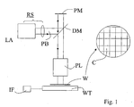
- FIG. 1 schematically depicts an imaging apparatus in conjunction with which the current invention can be employed.
- the apparatus comprises:
- the source LA may be within the housing of imaging apparatus, but that it may also be remote from the imaging apparatus, the radiation beam which it produces being led into the apparatus, e.g. with the aid of suitable directing mirrors.
- the current invention and Claims encompass both of these scenarios.
- the beam PB passes through the lens PL, which focuses the beam PB onto a target portion C of the substrate W.
- the substrate table WT can be moved accurately, e.g. so as to position different target portions C in the path of the beam PB.
- movement of the substrate table WT will be realized with the aid of a long-stroke module (coarse positioning) and a short-stroke module (fine positioning), which are not explicitly depicted in Figure 1 .
- the substrate W may, for example, a quartz plate onto which a mask pattern is to be written, or a silicon wafer onto which an array of device dies is to be imaged.
- Figure 2 depicts part of an imaging apparatus, whereby beam splitting means BS are employed between the patterning means PM and the substrate W, serving to divert aside a portion PB' of the projection beam PB and direct it onto image detection means ID.
- the beam splitting means BS should not be confused with the deflection means DM in Fig. 1 , which serve a different purpose.
- the beam splitting means BS can be located at any convenient point between items PM and W.
- the image detection means (e.g. comprising a CCD array) are used to analyze the pattern in the beam PB', with the purpose of determining whether or not it corresponds to the desired pattern to be produced by the patterning means PM. If not, imaging on the substrate W can be postponed or halted, and the patterning means PM reset and "re-fired" so as to produce the intended pattern anew, which is again checked using items BS and ID. In this way, one prevents imaging occurring on the basis of a faulty pattern, caused by a pixel error in the patterning means PM or their driving electronics, for example.
- the image detection means can, for example, be connected to a computer capable of performing image processing. Such a computer can then compare the pattern in the beam PB' with a reference pattern, and identify any discrepancies between the two.
- Figure 3 shows a first embodiment of the invention.
- reference patterning means PM2 e.g. a programmable mirror array of the same type and size as that in Figure 2
- main patterning means PM1 corresponding to item PM in Fig. 2
- the main patterning means PM1 and reference patterning means PM2 should then produce patterns that are identical, except in that they are each other's negative (or complement).
- the patterned beam PB2 produced by the reference patterning means PM2 is coupled into the beam splitting means BS, and ultimately onto the image detecting means ID.
- the patterned beams PB2 and PB 1 should add to produce an isotropic image of uniform brightness on the detector ID. However, if there is a pixel error, this will result in a spot of higher or lower intensity on the detector ID, which in turn will produce an error signal. This is a particularly elegant method of analyzing the output from the main patterning means PM1.
- Figure 4 shows a variant of the embodiment depicted in Figure 3 .
- the reference patterning means PM2 are situated between the beam splitting means BS and the detector ID.
- the reference patterning means PM2 are transmissive; however, they may also be reflective, without disturbing the principle of operation depicted in Fig. 4 .
Landscapes
- Physics & Mathematics (AREA)
- General Physics & Mathematics (AREA)
- Exposure And Positioning Against Photoresist Photosensitive Materials (AREA)
- Length Measuring Devices By Optical Means (AREA)
Priority Applications (1)
| Application Number | Priority Date | Filing Date | Title |
|---|---|---|---|
| EP02790447A EP1449032B1 (en) | 2001-11-27 | 2002-11-27 | Imaging apparatus |
Applications Claiming Priority (4)
| Application Number | Priority Date | Filing Date | Title |
|---|---|---|---|
| EP01204567 | 2001-11-27 | ||
| EP01204567 | 2001-11-27 | ||
| EP02790447A EP1449032B1 (en) | 2001-11-27 | 2002-11-27 | Imaging apparatus |
| PCT/EP2002/013399 WO2003046662A1 (en) | 2001-11-27 | 2002-11-27 | Imaging apparatus |
Publications (2)
| Publication Number | Publication Date |
|---|---|
| EP1449032A1 EP1449032A1 (en) | 2004-08-25 |
| EP1449032B1 true EP1449032B1 (en) | 2008-12-31 |
Family
ID=8181314
Family Applications (1)
| Application Number | Title | Priority Date | Filing Date |
|---|---|---|---|
| EP02790447A Expired - Lifetime EP1449032B1 (en) | 2001-11-27 | 2002-11-27 | Imaging apparatus |
Country Status (7)
| Country | Link |
|---|---|
| US (1) | US7379579B2 (enExample) |
| EP (1) | EP1449032B1 (enExample) |
| JP (1) | JP4290553B2 (enExample) |
| KR (1) | KR100674245B1 (enExample) |
| CN (1) | CN1294455C (enExample) |
| DE (1) | DE60230663D1 (enExample) |
| WO (1) | WO2003046662A1 (enExample) |
Cited By (1)
| Publication number | Priority date | Publication date | Assignee | Title |
|---|---|---|---|---|
| TWI494708B (zh) * | 2011-04-08 | 2015-08-01 | Asml Netherlands Bv | 微影裝置、可程式化之圖案化器件及微影方法 |
Families Citing this family (9)
| Publication number | Priority date | Publication date | Assignee | Title |
|---|---|---|---|---|
| EP1324138A3 (en) * | 2001-12-28 | 2007-12-19 | ASML Netherlands B.V. | Lithographic apparatus and device manufacturing method |
| JP4929444B2 (ja) * | 2004-09-27 | 2012-05-09 | 国立大学法人東北大学 | パターン描画装置および方法 |
| US7177012B2 (en) | 2004-10-18 | 2007-02-13 | Asml Netherlands B.V. | Lithographic apparatus and device manufacturing method |
| US7403865B2 (en) * | 2004-12-28 | 2008-07-22 | Asml Netherlands B.V. | System and method for fault indication on a substrate in maskless applications |
| US7233384B2 (en) * | 2005-06-13 | 2007-06-19 | Asml Netherlands B.V. | Lithographic apparatus and device manufacturing method, and device manufactured thereby for calibrating an imaging system with a sensor |
| EP1986224A4 (en) * | 2006-02-16 | 2012-01-25 | Nikon Corp | EXPOSURE APPARATUS, EXPOSURE METHOD, AND DEVICE MANUFACTURING METHOD |
| DE102011076083A1 (de) | 2011-05-18 | 2012-11-22 | Fraunhofer-Gesellschaft zur Förderung der angewandten Forschung e.V. | Projektionsdisplay und Verfahren zum Anzeigen eines Gesamtbildes für Projektionsfreiformflächen oder verkippte Projektionsflächen |
| JP6676942B2 (ja) * | 2015-12-01 | 2020-04-08 | 株式会社ニコン | 制御装置及び制御方法、露光装置及び露光方法、デバイス製造方法、データ生成方法、並びに、プログラム |
| TWI724642B (zh) * | 2019-11-20 | 2021-04-11 | 墨子光電有限公司 | 微製像設備及其加工方法 |
Family Cites Families (22)
| Publication number | Priority date | Publication date | Assignee | Title |
|---|---|---|---|---|
| GB2049964A (en) * | 1979-05-01 | 1980-12-31 | Agfa Gevaert Nv | Simultaneously projecting two images of a subject in register |
| DE3406677A1 (de) * | 1984-02-24 | 1985-09-05 | Fa. Carl Zeiss, 7920 Heidenheim | Einrichtung zur kompensation der auswanderung eines laserstrahls |
| JP2501436B2 (ja) * | 1986-10-31 | 1996-05-29 | 富士通株式会社 | パタ−ンデ−タ検査装置 |
| JP2796316B2 (ja) * | 1988-10-24 | 1998-09-10 | 株式会社日立製作所 | 欠陥または異物の検査方法およびその装置 |
| JPH03265815A (ja) * | 1990-03-16 | 1991-11-26 | Kobe Steel Ltd | レーザビームによる描画装置 |
| US5142132A (en) * | 1990-11-05 | 1992-08-25 | Litel Instruments | Adaptive optic wafer stepper illumination system |
| WO1992011567A1 (en) * | 1990-12-21 | 1992-07-09 | Eastman Kodak Company | Method and apparatus for selectively varying the exposure of a photosensitive medium |
| US5229889A (en) * | 1991-12-10 | 1993-07-20 | Hughes Aircraft Company | Simple adaptive optical system |
| US5229872A (en) | 1992-01-21 | 1993-07-20 | Hughes Aircraft Company | Exposure device including an electrically aligned electronic mask for micropatterning |
| JP2710527B2 (ja) * | 1992-10-21 | 1998-02-10 | 大日本スクリーン製造株式会社 | 周期性パターンの検査装置 |
| JPH06250108A (ja) * | 1993-02-22 | 1994-09-09 | Hitachi Ltd | 補償光学装置とこれを用いた天体望遠鏡,光データリンク,レーザ加工機 |
| JPH088161A (ja) * | 1994-06-20 | 1996-01-12 | Mitsubishi Electric Corp | 転写シミュレータ装置 |
| US6133986A (en) * | 1996-02-28 | 2000-10-17 | Johnson; Kenneth C. | Microlens scanner for microlithography and wide-field confocal microscopy |
| JPH10177589A (ja) * | 1996-12-18 | 1998-06-30 | Mitsubishi Electric Corp | パターン比較検証装置、パターン比較検証方法およびパターン比較検証プログラムを記録した媒体 |
| JP4159139B2 (ja) * | 1998-05-14 | 2008-10-01 | リコーマイクロエレクトロニクス株式会社 | 光像形成装置、光加工装置並びに露光装置 |
| SE519397C2 (sv) * | 1998-12-16 | 2003-02-25 | Micronic Laser Systems Ab | System och metod för mikrolitografiskt ritande av högprecisionsmönster |
| JP3315658B2 (ja) | 1998-12-28 | 2002-08-19 | キヤノン株式会社 | 投影装置および露光装置 |
| TWI282909B (en) * | 1999-12-23 | 2007-06-21 | Asml Netherlands Bv | Lithographic apparatus and a method for manufacturing a device |
| JP2001255664A (ja) * | 2000-03-14 | 2001-09-21 | Fuji Photo Film Co Ltd | 画像露光方法 |
| JP4364459B2 (ja) * | 2000-12-07 | 2009-11-18 | 富士通株式会社 | 光信号交換器の制御装置および制御方法 |
| JP2002367900A (ja) * | 2001-06-12 | 2002-12-20 | Yaskawa Electric Corp | 露光装置および露光方法 |
| KR20040047816A (ko) * | 2001-09-12 | 2004-06-05 | 마이크로닉 레이저 시스템즈 에이비 | 공간광변조기를 이용한 개선된 방법 및 장치 |
-
2002
- 2002-11-27 KR KR1020047007941A patent/KR100674245B1/ko not_active Expired - Fee Related
- 2002-11-27 CN CNB028235606A patent/CN1294455C/zh not_active Expired - Fee Related
- 2002-11-27 JP JP2003548035A patent/JP4290553B2/ja not_active Expired - Fee Related
- 2002-11-27 WO PCT/EP2002/013399 patent/WO2003046662A1/en not_active Ceased
- 2002-11-27 EP EP02790447A patent/EP1449032B1/en not_active Expired - Lifetime
- 2002-11-27 US US10/496,630 patent/US7379579B2/en not_active Expired - Fee Related
- 2002-11-27 DE DE60230663T patent/DE60230663D1/de not_active Expired - Lifetime
Cited By (1)
| Publication number | Priority date | Publication date | Assignee | Title |
|---|---|---|---|---|
| TWI494708B (zh) * | 2011-04-08 | 2015-08-01 | Asml Netherlands Bv | 微影裝置、可程式化之圖案化器件及微影方法 |
Also Published As
| Publication number | Publication date |
|---|---|
| KR20040054804A (ko) | 2004-06-25 |
| CN1294455C (zh) | 2007-01-10 |
| JP2005510860A (ja) | 2005-04-21 |
| EP1449032A1 (en) | 2004-08-25 |
| CN1596387A (zh) | 2005-03-16 |
| DE60230663D1 (de) | 2009-02-12 |
| KR100674245B1 (ko) | 2007-01-25 |
| US7379579B2 (en) | 2008-05-27 |
| WO2003046662A1 (en) | 2003-06-05 |
| US20050062948A1 (en) | 2005-03-24 |
| JP4290553B2 (ja) | 2009-07-08 |
Similar Documents
| Publication | Publication Date | Title |
|---|---|---|
| US7560196B2 (en) | Mask for exposing an alignment mark, and method and computer program for designing the mask | |
| US7466413B2 (en) | Marker structure, mask pattern, alignment method and lithographic method and apparatus | |
| US7019814B2 (en) | Lithographic projection mask, device manufacturing method, and device manufactured thereby | |
| US7046331B2 (en) | Lithographic apparatus, device manufacturing method, and device manufactured thereby | |
| EP1449032B1 (en) | Imaging apparatus | |
| EP1467252A1 (en) | Device manufacturing method and mask set for use in the method | |
| EP1480086A1 (en) | Lithographic apparatus and device manufacturing method | |
| US6891598B2 (en) | Lithographic device and method for wafer alignment with reduced tilt sensitivity | |
| EP1260870A1 (en) | Alignment mark | |
| EP1353230A1 (en) | Device manufacturing method and computer programs | |
| US7041996B2 (en) | Method of aligning a substrate, a computer program, a device manufacturing method and a device manufactured thereby | |
| EP1260869A1 (en) | Substrate provided with an alignment mark in a substantially transparent process layer | |
| EP1324137B1 (en) | Device manufacturing method, device manufactured thereby and lithographic apparatus therefor | |
| EP1431834B1 (en) | A device manufacturing method using a lithographic projection mask | |
| EP1353234A1 (en) | Device manufacturing method, device manufactured thereby and computer program | |
| EP1498779A2 (en) | Marker structure for alignment or overlay | |
| EP1398670A2 (en) | A method of aligning a substrate, a computer program and a device manufacturing method | |
| EP1353233A2 (en) | Lithographic apparatus and device manufacturing method |
Legal Events
| Date | Code | Title | Description |
|---|---|---|---|
| PUAI | Public reference made under article 153(3) epc to a published international application that has entered the european phase |
Free format text: ORIGINAL CODE: 0009012 |
|
| 17P | Request for examination filed |
Effective date: 20040512 |
|
| AK | Designated contracting states |
Kind code of ref document: A1 Designated state(s): AT BE BG CH CY CZ DE DK EE ES FI FR GB GR IE IT LI LU MC NL PT SE SK TR |
|
| RAP1 | Party data changed (applicant data changed or rights of an application transferred) |
Owner name: ASML NETHERLANDS B.V. |
|
| 17Q | First examination report despatched |
Effective date: 20071129 |
|
| GRAP | Despatch of communication of intention to grant a patent |
Free format text: ORIGINAL CODE: EPIDOSNIGR1 |
|
| RTI1 | Title (correction) |
Free format text: IMAGING APPARATUS |
|
| GRAS | Grant fee paid |
Free format text: ORIGINAL CODE: EPIDOSNIGR3 |
|
| GRAS | Grant fee paid |
Free format text: ORIGINAL CODE: EPIDOSNIGR3 |
|
| GRAA | (expected) grant |
Free format text: ORIGINAL CODE: 0009210 |
|
| AK | Designated contracting states |
Kind code of ref document: B1 Designated state(s): DE FR GB IT NL |
|
| REG | Reference to a national code |
Ref country code: GB Ref legal event code: FG4D |
|
| REF | Corresponds to: |
Ref document number: 60230663 Country of ref document: DE Date of ref document: 20090212 Kind code of ref document: P |
|
| PG25 | Lapsed in a contracting state [announced via postgrant information from national office to epo] |
Ref country code: NL Free format text: LAPSE BECAUSE OF FAILURE TO SUBMIT A TRANSLATION OF THE DESCRIPTION OR TO PAY THE FEE WITHIN THE PRESCRIBED TIME-LIMIT Effective date: 20081231 |
|
| NLV1 | Nl: lapsed or annulled due to failure to fulfill the requirements of art. 29p and 29m of the patents act | ||
| PLBE | No opposition filed within time limit |
Free format text: ORIGINAL CODE: 0009261 |
|
| STAA | Information on the status of an ep patent application or granted ep patent |
Free format text: STATUS: NO OPPOSITION FILED WITHIN TIME LIMIT |
|
| 26N | No opposition filed |
Effective date: 20091001 |
|
| GBPC | Gb: european patent ceased through non-payment of renewal fee |
Effective date: 20091127 |
|
| PG25 | Lapsed in a contracting state [announced via postgrant information from national office to epo] |
Ref country code: GB Free format text: LAPSE BECAUSE OF NON-PAYMENT OF DUE FEES Effective date: 20091127 |
|
| PG25 | Lapsed in a contracting state [announced via postgrant information from national office to epo] |
Ref country code: IT Free format text: LAPSE BECAUSE OF FAILURE TO SUBMIT A TRANSLATION OF THE DESCRIPTION OR TO PAY THE FEE WITHIN THE PRESCRIBED TIME-LIMIT Effective date: 20081231 |
|
| REG | Reference to a national code |
Ref country code: FR Ref legal event code: PLFP Year of fee payment: 14 |
|
| REG | Reference to a national code |
Ref country code: FR Ref legal event code: PLFP Year of fee payment: 15 |
|
| PGFP | Annual fee paid to national office [announced via postgrant information from national office to epo] |
Ref country code: DE Payment date: 20161121 Year of fee payment: 15 Ref country code: FR Payment date: 20161118 Year of fee payment: 15 |
|
| REG | Reference to a national code |
Ref country code: DE Ref legal event code: R119 Ref document number: 60230663 Country of ref document: DE |
|
| REG | Reference to a national code |
Ref country code: FR Ref legal event code: ST Effective date: 20180731 |
|
| PG25 | Lapsed in a contracting state [announced via postgrant information from national office to epo] |
Ref country code: FR Free format text: LAPSE BECAUSE OF NON-PAYMENT OF DUE FEES Effective date: 20171130 Ref country code: DE Free format text: LAPSE BECAUSE OF NON-PAYMENT OF DUE FEES Effective date: 20180602 |